

Abstract
Laser diodes employing strain-compensated GaAs1−xBix/GaAs1−yPy quantum well (QW) active regions were grown by metalorganic vapor phase epitaxy (MOVPE). High resolution x-ray diffraction, room temperature photoluminescence, and in situ optical reflectance monitoring during the MOVPE growth provided valuable feedback for the optimization of the material growth conditions. In addition, the post-growth in situ thermal annealing was employed to improve the radiative efficiency of the GaAs1−xBix/GaAs1−yPy QW structures. Wide ridge waveguide lasers with GaAs barriers exhibited high threshold current densities (Jth ∼ 8 kA cm−2), excessive band-filling, and carrier leakage at room temperature, resulting in the lasing from a high energy transition. By contrast, devices employing GaAs1−yPy barriers exhibited significantly lower threshold current densities (Jth ∼ 5.9 kA cm−2), and longer wavelength QW emission, presumably as a result of improved active region carrier confinement. Devices with GaAs0.8P0.2 barriers after the post-growth thermal annealing exhibited further reduced threshold current density (Jth ∼ 4.1 kA cm−2).
Export citation and abstract BibTeX RIS
1. Introduction
There have been extensive studies on the GaAs1−xBix alloy system grown by molecular beam epitaxy (MBE) or metal organic vapor phase epitaxy (MOVPE) on GaAs for applications to microelectronic and optoelectronic devices [1–4]. Previously reported experimental and theoretical results have shown that a small amount of Bi incorporation into GaAs induces a rapid reduction in the band gap ( ) (62–84 meV per Bi mole fraction) and an increase in spin–orbit splitting
  with increasing Bi within the dilute bismide GaAs1−xBix alloy [5–8]. This large bandgap reduction and an increase in
  which can therefore suppress hot-hole driven Auger recombination and intervalence band absorption at high Bi concentration
  [2], can allow GaAs1−xBix quantum well (QW) active regions to be a suitable candidate for achieving high-efficiency lasers in the telecom wavelength regions (λ ∼ 1.3–1.55 μm) on GaAs substrates as an alternate approach to InAs quantum dots or dilute-nitride QWs.
The origin of this rapid band gap bowing effect has been attributed to the interaction between the localized Bi resonant level and the valence band of GaAs within a valence band anti-crossing model, leading to a large valence band offset (∼55 meV/%Bi) and a relatively small conduction band offset (∼15 meV/%Bi) at the GaAs1−xBix/GaAs heterojunction, particularly at low Bi mole fraction [9]. For the application where the both electron and hole confinement is required, such as an active region within a laser diode structure, it is necessary to choose a higher bandgap material as an electron barrier. The first successful operation of an electrically injected GaAs1−zBiz single quantum well (SQW) laser with the lasing wavelength of 947 nm was reported by Ludewig et al [2]. Subsequently, there have been several other reports of diode lasers employing GaAs1−zBiz in the active region, confirming the potential of this material as a light-emitting source in near-IR region [10–12]. In these prior studies, AlxGa1−xAs was used as a barrier material for low Bi-content QWs to improve the electron confinement in the conduction band and reduce thermally activated carrier leakage from the QW. We investigate here the use of tensile-strained GaAs1−yPy as a QW barrier material, since an Al-free alloy is generally more compatible with the low growth temperatures required for the Bi-containing materials. As schematically shown in figure 1, the GaAs1−xBix/GaAs1−yPy QW structures can provide a sufficient conduction band offset and subsequently strong electron confinement within the QW, and offer a pathway, through the thickness and composition, to engineer the average strain of the active region, leading to strain-balancing [13]. This strain-balancing is particularly of importance for structures employing the multiple quantum well (MQW) and/or high bismuth concentrations, to prevent a strain relaxation [14]. Another motivating factor is that the previous report has shown that the use of the tensile-strained GaAs0.67P0.33 barriers is effective in enhancing carrier confinement to the compressive-strained dilute-nitride (InxGa1−xAsyN1−y) QW laser active regions, thus improving the temperature sensitivity of the device and resulting in higher device performance [15]. Here, we report on the optical and electronic properties of the MOVPE-grown single QW GaAs0.975Bi0.025 active region laser diodes with tensile-strained GaAs0.8P0.2 barriers.

Figure 1. Schematic band diagram for (a) GaAs1−xBix/GaAs heterostructure, and (b) GaAs1−xBix/GaAs1−yPy heterostructure.
Download figure:
Standard image High-resolution image2. Material growth and experimental details
The metastable nature of the GaAs1−xBix alloy, which exhibits a large miscibility gap, requires the material growth to be performed far away from thermodynamic equilibrium [16]. This restriction compels the growth of GaAs1−xBix to be performed with non-typical growth parameters, involving the low growth temperature around 400  C and near-stoichiometric V/III flux ratio for MBE and gas-phase ratio for MOVPE for the Bi incorporation into the host GaAs matrix [17, 18]. In turn, the growth under the near-stoichiometric condition at such a low temperature can result in point defects and its associated defect complexes, which can act as non-radiative recombination centers within the materials [19]. In addition, particularly for the MOVPE growth, the low growth temperature can lead to high unintentional background carbon contamination as the hydrocarbon radicals from the metal-organic precursors, which are not effectively removed from the growth front, leads to an increased carbon incorporation [17]. This unintentional background carbon has been shown to reduce the minority carrier lifetime [20]. For these reasons, the growth parameters should be carefully optimized for the MOVPE growth of device quality GaAs1−xBix films.
The material growth in this study was performed, using a close-coupled-showerhead vertical reactor with a rotating susceptor. The growth was monitored in situ by the optical reflectance system by Laytec's EpiTT™. For the GaAs1−xBix growth, triethyl-gallium(TEGa) was used as group III precursors while tertiarybutyl-arsine(TBAs), and trimethyl-bismuth(TMBi) were used for group V precursors. For the growth optimization, samples consisting of 5 period MQW (5x GaAs1−xBix/GaAs) were grown on nominally exact (100) semi-insulating GaAs substrates (within ± 0.1°) with varying growth temperature (Tgrowth) and varying TMBi/V gas phase ratio. All precursors were fed into the reactor simultaneously. After the GaAs1−xBix QW growth, the growth temperature was raised to 630  C under arsine/H2 ambient, and the GaAs barrier was grown with trimethyl-gallium (TMGa) and arsine(AsH3). The growth parameters are summarized in the table 1. This temperature ramping was employed in previous studies, and is thought to lead to evaporation of the surface-segregated Bi on the growing GaAs1−xBix film [2, 21]. Photoluminescence (PL) measurements at room temperature were used in order to evaluate the luminescence properties of each sample. For the PL measurement, the frequency doubled continuous wave Nd:YAG laser (532 nm) as a excitation source, 300 g mm−1 grating monochromator, and liquid nitrogen cooled InGaAs detectors were used. In order to investigate the structural properties of the MQW structure, high resolution x-ray diffraction (HR-XRD) ω–2θ scans around the GaAs (004) reflection were used. After finding an optimized growth condition, the laser diode structures were grown on nominally exact n+ GaAs substrates as shown in figure 2. For the growth of GaAs0.8P0.2, TMGa, AsH3 and Phosphine(PH3) were used as precursors. Trimethyl-aluminum, TMGa, and AsH3 were used for the (Al)GaAs growth within the laser structures. Disilane (Si2H6) was used as a n-dopant while carbon tetrabromide (CBr4) was used for p-dopant in the Al0.65Ga0.35As upper cladding layer, and diethyl-zinc was used for heavily doped p+ GaAs contact layer. To investigate the effect of the high bandgap GaAs1-yPy barrier on the electronic and optical properties, one laser diode structure was grown without P (y = 0), while another laser diode was grown with y = 0.2 within the GaAs1−yPy barrier. The optical confinement factor for this structure was calculated to be 2.4%. After the laser structure growth, the wafers were cleaved and one of each sample were subjected to an additional in situ annealing within the MOVPE reactor under AsH3 (3.8 mmol min−1) for 25 min. The high-angle annular dark-field (HAADF), or 'z-contrast', imaging method in an aberration corrected scanning transmission electron microscopy (STEM) measurement was used to investigate the homogeneity of the Bi distribution and interfacial abruptness within the annealed laser structure.
Table 1. Growth parameters used for the material optimization.
| Material | Pressure (Torr) | Growth temp. (°C) | TEGa (μmol min−1) | TMBi/TBAs | V/III ratio |
|---|---|---|---|---|---|
| QW (GaAs1−xBix) | 50 | 400–440 | 133 | 0.023 ∼ 0.036 | 1.31 |
| Barrier (GaAs) | 100 | 630 | TMGa used (55 μmol min−1) | N/A | 60–70 |
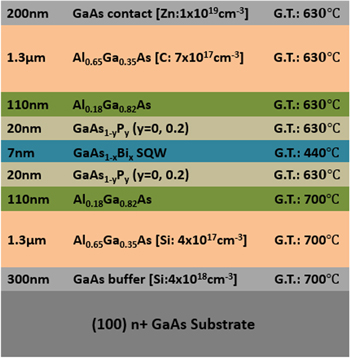
Figure 2. Complete laser diode structure. The growth temperature is denoted as G. T.
Download figure:
Standard image High-resolution image25 μm wide ridge waveguide lasers were fabricated by a standard photolithographic process from both the as-grown and annealed samples. The wet etching using H3PO4:H2O2:H2O = 3:1:20 was carried out to form the etched ridge waveguide structure, using a patterned photoresist mask. 200 nm thick SiNx was deposited by plasma-enhanced chemical vapor deposition for the electrical passivation. The wafer was subsequently thinned down to 150 μm. Contact layers consisting of Ti/Pt/Au (25/50/300 nm) were e-beam evaporated on the top surface to form the ohmic contact to p+ GaAs. Contact to the n-type region was made to the backside of the wafer using a Ni/AuGe/Ni/Au (5/100/35/200 nm) contact metallurgy. The contact metals were alloyed at 400 °C for 30 s using rapid thermal annealing. Devices were measured as-cleaved (i.e. no facet coatings) at room temperature and 80 K under pulsed current operation. The electroluminescence (EL) data was collected using a grating diffractometer and Si photodetector while the output power from one facet were measured using InGaAs photodiode.
3. Results and discussion
The Bi incorporation as a function of the growth temperature was investigated by varying only the growth temperature from 400 °C to 440  C while maintaining other growth parameters including TEGa molar flow (133 μmol min−1), TMBi/TBAs = 0.036, reactor pressure (Preactor = 50 Torr), and V/III ratio. Presented in figure 3(a) are the HR-XRD spectra, which possess a sharp contrast in both pendellosung oscillations and the satellite peaks for all samples. These XRD measurements suggest that even with temperature ramping between well and barrier, it is possible to achieve an abrupt GaAs1−xBix/GaAs heterointerface, which agrees well with the previous reports [2, 21]. Assuming a GaBi zincblende lattice constant of 0.633 nm, the GaBi mole fractions of each sample was found from comparing the x-ray spectra to the XRD dynamic simulations at a point of best fit to the experimental HR-XRD data [18]. The structural details of each sample derived from the XRD simulations are summarized in table 2. The PL measurements, shown in figure 3(b), indicate a rapid increase in the PL intensities and spectral blueshifts as the Tgrowth increases. This result can possibly be attributed to a combination of effects including a decrease in the Bi-related defect concentration as a result of the reduced Bi incorporation, reduction in other point defects and defect complexes associated with near-stoichiometric growth, and a lower background carbon concentration resulting from a higher Tgrowth. Our observations agree well with the study by Ludewig et al [22], although it should be noted that their QW structures were grown by the pulsed growth mode.
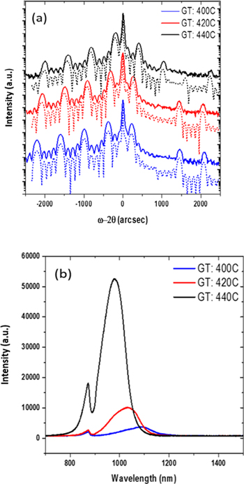
Figure 3. (a) HR-XRD ω–2θ measured around GaAs (004) reflection, indicating fully strained 5x GaAs1−xBix/GaAs MQWs. Dynamic XRD simulations are indicated by the dotted lines for each sample. (b) Photoluminescence measured at room temperature.
Download figure:
Standard image High-resolution imageTable 2. Structure details and GaAs1−xBix growth rate as a function of growth temperature.
| Growth temperature (°C) | Structure details from the HR-XRD dynamic simulation | GaAs1−xBix growth rate (nm s−1) | PL peak position (eV) |
|---|---|---|---|
| 400 | 5x GaAs0.957Bi0.043/GaAs (9/22 nm) | 0.036 | 1.114 |
| 420 | 5x GaAs0.966Bi0.034/GaAs (10/22 nm) | 0.067 | 1.2 |
| 440 | 5x GaAs0.974Bi0.026/GaAs (9/22 nm) | 0.1 | 1.261 |
A study of the effect of gas-phase TMBi/V ratio on the luminescence properties of the GaAs1−xBix QWs was carried out. For this study, only the TMBi molar flow was adjusted while fixing other growth parameters such as TEGa molar flow (133 μmol min−1), TBAs molar flow (174 μmol min−1), Tgrowth (440 °C), and Preactor (50 Torr). Shown in figure 4(a) are the HR-XRD measurements and their corresponding dynamic simulations, which indicate a reduction in the growth rate as TMBi/V ratio increases. Table 3 summarizes the structure details and their growth rates of each samples, deduced from the fitting of the XRD dynamic simulation to the experimental HR-XRD data. This decrease in growth rate is most likely due to the segregated Bi at the growth front, which can block surface sites, preventing the incorporation of Ga, as previously reported elsewhere [17].
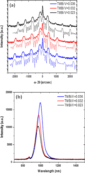
Figure 4. (a) HR-XRD ω–2θ measured around GaAs (004) reflection, indicating fully strained 5x GaAs1–xBix/GaAs MQWs. Dynamic XRD simulations are indicated by the dotted lines for each sample. (b) Photoluminescence measured at room temperature.
Download figure:
Standard image High-resolution imageTable 3. Structure details and GaAs1−xBix growth rate as a function of TMBi/V molar flow rate.
| TMBi/V molar flow ratio | Structure details from the HR-XRD dynamic simulation | GaAs1−xBix growth rate (nm s−1) | Growth time (s) | PL peak position (eV) |
|---|---|---|---|---|
| 0.023 | 5x GaAs0.983Bi0.017/GaAs (12/23 nm) | 0.134 | 90 | 1.28 |
| 0.032 | 5x GaAs0.975Bi0.025/GaAs (7/23 nm) | 0.105 | 67 | 1.27 |
| 0.036 | 5x GaAs0.974Bi0.026/GaAs (9/22 nm) | 0.1 | 90 | 1.261 |
The in situ reflectance taken during the growth also indicates that the growth rate is reduced at a high TMBi/V ratio, as evidenced by the real-time optical reflectance including the plateau, indicating slower or no growth, as shown in the figure 5(c). Again, this is attributed to the excess Bi at the growth front. As a result, the sample surface with TMBi/V = 0.036 contains Bi containing droplets, while the other samples exhibit a droplet-free surface.

Figure 5. Reflectance measured in situ during the growth. The shaded area corresponds to the growth of GaAs1−xBix QWs. (a) in situ reflectance during the growth with TMBi/V = 0.023, (b) in situ reflectance during the growth with TMBi/V = 0.032, and (c) in situ reflectance during the growth with TMBi/V = 0.036.
Download figure:
Standard image High-resolution imageIt should be noted that the small decrease in the TMBi/V ratio from 0.036 to 0.032 does not significantly decrease the GaBi mole fraction in the solid, as summarized in table 3. Based on the trend deduced from the growths of TMBi/V = 0.023 and 0.032, the expected solid GaBi mole fraction with TMBi/V = 0.036 is 2.8% while the measured solid GaBi mole fraction is 2.6%. This implies that the growths under the TMBi/V of 0.032–0.036 take place within or at the onset of the 'saturated regime', where solid GaBi mole fraction in the growing layer is independent of the input TMBi/V ratio above a certain ratio [23]. The reduction in the background carbon concentration observed when using a high TMBi/V ratio has also been reported, and again has been ascribed to an effect of the surface segregated Bi, blocking surface reaction sites [24]. Our observation of an increased PL intensity from the samples with the higher TMBi ratio, shown in figure 4(b), could be attributed to this effect.
For a laser structure, it is important to have abrupt interfaces between QWs and barriers, without the Bi droplets, which could lead to current leakage paths. Therefore, in order to avoid the droplet formation, a TMBi/V = 0.032 was chosen for the further study. To investigate the effect of the GaAs0.8P0.2 barrier on the luminescence properties, a 5x GaAs0.975Bi0.025/GaAs0.8P0.2 (8/15 nm) structure was grown in the similar manner to the samples grown with GaAs barriers, i.e., temperature ramping to a higher growth temperature was used when growing the GaAs0.8P0.2 barrier after the growth of the GaAs0.975Bi0.025 QW. From the PL measurements, shown in figure 6(a), it was found that the sample with the GaAs0.8P0.2 barrier exhibits and improved PL intensity with a slight blueshift, most likely due to the higher electron confinement in the QW. Also, in situ annealing at 630 °C for 40 min, which represents the typical growth time for the upper cladding layer and contact layer growth in a laser diode structure, under AsH3 on this structure did not result in a noticeable spectral shift in the PL spectra while an improved PL intensity was observed, as shown in figure 6(a). The HR-XRD spectra measured before and after in situ annealing also did not show any evidence of significant layer intermixing.
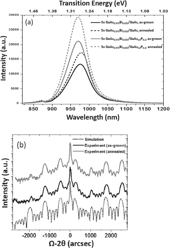
Figure 6. (a) RT-PLs from the as grown and annealed 5-period MQW samples with GaAs (5x GaAs0.975Bi0.025/GaAs, 7/22 nm) and GaAs0.8P0.2 barriers (5x GaAs0.975Bi0.025/GaAs, 8/15 nm), (b) HR-XRD measurement and the dynamic simulation for the as-grown and annealed 5x GaAs0.975Bi0.025/GaAs0.8P0.2 (8/15 nm) MQW sample.
Download figure:
Standard image High-resolution imageBoth EL and light output versus current input (PI) were measured from both annealed and as-grown samples, as shown in figure 7. These samples possessed either GaAs or GaAs0.8P0.2 barriers and a SQW GaAs0.975Bi0.025 grown under conditions of TMBi/V = 0.032 at Tgrowth = 440  C. For the structure with GaAs0.8P0.2 barriers, the laser diodes from both as-grown and annealed samples operated at room temperature with a conventional threshold current (Ith) behavior and the narrowed full-width-half-max above the threshold current. A strong reduction in the threshold current density (Jth) was observed from the device with in situ annealing, as compared to the as-grown devices. However, the Jth = 4.1 kA cm−2 from the annealed device was still higher than the previously lowest reported value of Jth = 1–1.1 kA cm−2 [12]. It should be noted that the GaBi mole fraction within the SQW laser structure employed in the previous study [12] was x = 0.022 while the current devices employ x = 0.025 which results in a longer lasing wavelength (λlasing = 962 nm versus 947 nm). Therefore, the higher Jth observed here could be attributed to a higher concentration of Bi-related defects. The reduction in Jth after annealing is most likely a result of a reduction in the point defect concentration within the GaAs0.975Bi0.025 SQW. The characteristic temperature, T0, was measured from 20 °C to 60
  C from the devices with GaAs0.8P0.2 barriers fabricated from the annealed material as shown in figure 8. The measured T0
  60 K, which was lower than that of the reported value
  [12] suggests that a higher P content in the GaAs1−yPy barrier is necessary to effectively suppress the thermionic leakage [15]. It is worthwhile mentioning that the spectral shift as a function of varying temperature,
  was measured as 0.16 nm K−1, and was close to the reported value for bulk-like MBE grown dilute bismide lasers (0.17 nm K−1) [10]. This low temperature sensitivity of the lasing wavelength has been theoretically predicted in a prior study [25] and agrees well with the reported experimental temperature dependency of the GaAs1−xBix band gap [26]. Figure 9 presents a cross-sectional HAADF STEM image of the annealed GaAs0.975Bi0.025/GaAs0.8P0.2 laser diode sample, which suggests planar and abrupt interfaces with the homogenous Bi containing QW. For the devices with GaAs barriers, a lasing emission at higher transition energy, corresponding to 1.39 eV, was observed at room temperature. At low drive current, the EL peak was positioned at lower transition energy, as shown in figure 10(a). This result suggests that excessive band-filling and thermionic leakage exist within the QW structure. Similar behavior was observed by Marko et al, where they experimentally demonstrated that this higher transition energy emission corresponds to the e1–lh1 (light hole) transition [27].
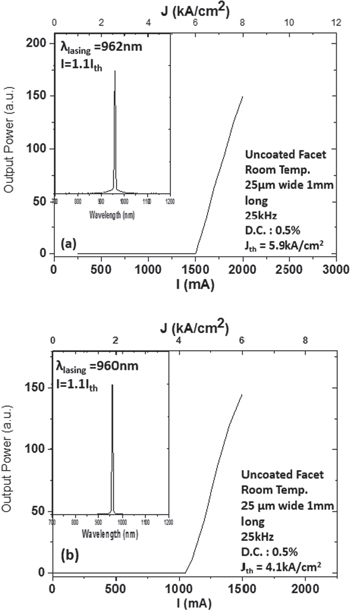
Figure 7. (a) PI and the spectrum(inset) of as-grown laser diode device employing GaAs0.975Bi0.025/GaAs0.8P0.2, (b) PI and the spectrum (inset) of annealed laser diode device employing GaAs0.975Bi0.025/GaAs0.8P0.2.
Download figure:
Standard image High-resolution image
Figure 8. (a) The PI curves obtained from the annealed GaAs0.975Bi0.025/GaAs0.8P0.2 device, and (b) the spectral shifts measured at I = 1.1Ith as a function of temperature from 20 °C to 60 C.
C.
Download figure:
Standard image High-resolution image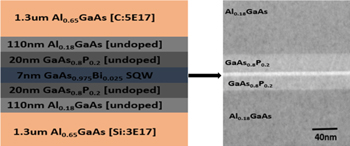
Figure 9. HAADF micrograph of the laser structure. 8 nm GaAs0.975Bi0.025 QW layer is cladded by GaAs0.8P0.2 barriers.
Download figure:
Standard image High-resolution image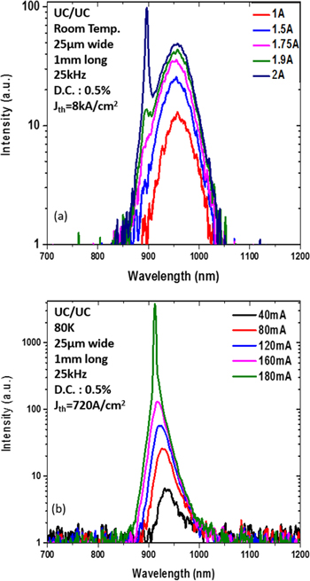
Figure 10. Spectra of the annealed GaAs0.975Bi0.025/GaAs devices measured at (a) room temperature, (b) 80 K.
Download figure:
Standard image High-resolution image
In contrast, as presented in figure 10(b), the measured spectrum at 80 K on the devices with GaAs barriers does not exhibit excessive band filling. The measured threshold current density at 80 K was Jth = 720 A cm−2. While this value is quite high, it is smaller than the previously reported Jth  1.4 kA cm−2 measured at 20 K from the device employing GaAs barriers in [12]. The observed lower Jth (Jth = 720 A cm−2 versus 1.4 kA cm−2 in [12]) at a higher operating temperature (80 K versus 20 K in [12]) could be partially ascribed to the higher optical confinement factor, 2.4%, in our study compared to ∼1.6% in [12]. Also, it should be noted that at 80 K, the electron thermal energy corresponds to 6.89 meV, which is significantly smaller than the conduction band offset at the heterointerface of GaAs0.975Bi0.025/GaAs. Therefore, one can expect minimal thermionic leakage at 80 K. This suggests that a significant carrier loss via non-radiative recombination exists within the GaAs1−xBix SQW, contributing to the relatively large measured Jth at 80 K.
Additional investigations focused on optimizing the material growth are necessary to reduce non-radiative recombination and achieve a further reduction in Jth. A more systematic study on the post-growth thermal annealing and the use of alternative Bi precursor such as triethyl-bismuth for reducing background carbon impurity concentration will also be needed to achieve a lower threshold current density.
4. Conclusion
HR-XRD, RT-PL, and in situ optical reflectance measurements were used to provide feedback in order to optimize the MOVPE growth of GaAs1−xBix MQW and SQW laser diodes. The characteristics of the GaAs0.975Bi0.025 SQW laser diodes with either a GaAs barrier or a higher bandgap GaAs0.8P0.2 barrier were measured. GaAs0.975Bi0.025/GaAs0.8P0.2 SQW active region lasers exhibited a reduction in Jth after a post-growth in situ thermal annealing. These improved characteristics most likely result from a reduction in the point defects concentration. Point defects and Bi-related defects can act as non-radiative recombination centers. The devices with a GaAs barrier structure show excessive carrier band-filling and thermionic leakage at room temperature associated with a low conduction band offset, resulting in lasing emission at a higher transition energy. These experimental results suggest the use of tensile-strained GaAs0.8P0.2 can enable both strain-balancing and electron and hole confinements within the QW. Further investigation on reducing Jth by optimizing the post-growth in situ thermal annealing and material growths is necessary.
Acknowledgments
This work is supported primarily by University of Wisconsin Materials Research Science and Engineering Center (DMR-1121288).