

Abstract
In this paper we study the feasibility of Fe(Se, Te) coated conductors on a simple rolling-assisted biaxially textured substrate (RABiTS) template. Starting from commercially available Ni–5 at% W tapes which show an out-of-plane orientation of about 7° and an in-plane orientation around 5°, we realized a RABiTS template for Fe(Se, Te) coated conductor fabrication by depositing CeO2 thin films on the metallic tape. The oxide buffer layers, deposited via pulsed laser ablation, exhibit an out-of-plane and an in-plane orientation suitable for Fe(Se, Te) deposition and act as a chemical barrier against Ni diffusion. Fe(Se, Te) thin films deposited on such a simple template show a superconducting transition at 16 K and very high upper critical field values with a ΔTc,0 of only 3 K in 18 T. The transport critical current reaches values of 1.7 × 10⁵ A cm−2 at 4.2 K in self-field and is reduced by less than one order of magnitude up to 18 T, remaining isotropic with respect to the magnetic field direction.
Export citation and abstract BibTeX RIS
1. Introduction
Iron-based superconductors (IBS), which were discovered ten years ago, exhibit a relatively high critical temperature Tc and huge upper critical fields Hc2, and have proved to have a great potential for high-field applications [1]. Among all the IBS families, the iron chalcogenides FeSexTe1−x, also called 11 phase or FST in the following, are the simplest, and they are quite attractive because of their relative ease of fabrication and the absence of toxic arsenic. FST thin films have been successfully grown on single crystalline substrates [2–4] and on technical metallic templates which have been developed and are already commercially available for the deposition of REBa2Cu3O7−x (REBCO, with RE = rare earth or Y) and present a quite complex architecture [5]. In particular, 11 thin films have been grown either on ion beam assisted deposition (IBAD) [6] and rolling-assisted biaxially textured substrate (RABiTS) [7] templates, showing values of critical current densities (Jc) as high as 105 A cm−2 up to 30 T [7]. The route to the realization of long conductors is still long though.
In IBS the exponential decay of Jc across misoriented grain boundaries seems to be less severe than for REBCO [5], in particular for Fe(Se, Te) thin films grown on bicrystals a misorientation angle θc ∼ 9° has been reported [8, 9], significantly higher than the θc ≈ 4° observed in REBCO. Moreover, Fe(Se, Te) thin films are deposited without the presence of oxygen in a temperature range between 230 °C and 550 °C [4], much below the deposition temperature required for REBCO. These features have a strong impact on the development of a suitable coated conductor (CC) technology, significantly relaxing the film texture constraint and the role of the buffer layer architecture. Hence, it is possible to think about the development of much simpler metallic templates, essentially reducing the complexity and the manufacturing cost of IBS-CC, which may make them more attractive on a cost–performance basis.
In a previous work, we studied the feasibility of producing 11 CCs by the deposition of thin films directly on a Ni–Fe alloy (namely, a biaxially oriented Invar 36 substrate) without a buffer layer but, despite the good orientation of the films, a significant Ni diffusion from the substrate to the film inhibited the superconductivity [10].
In this paper, we investigate the deposition of FST thin films on a very simple template, consisting of a Ni–5 at% W alloy RABiTS substrate with a single CeO2 layer on top, which can also act as a chemical barrier against Ni diffusion. In particular, we describe the deposition of a CeO2 buffer layer and 11 thin films via pulsed laser deposition (PLD) on Ni–5 at% W biaxially textured tapes. Moreover, we performed a study into the texturing of both the buffer and the film together with the characterization of the superconducting properties of the CCs, such as the upper critical field and the critical current density up to 18 T. In spite of the simplicity of the conductor architecture, 11 thin films show relevant superconducting properties with a Tc as high as 16 K, and isotropic transport critical current density values exceeding 105 A cm−2 at 4.2 K. Considering the large optimization margin, these results are encouraging for further improvement of a simple, low-cost, IBS based CC technology.
2. Experimental details
For the development of 11 CCs we used commercially available cube textured Ni–5 at% W (Ni–W) tapes from Evico as substrates [11]. On top of Ni–W we deposited CeO2 films, employed as a buffer layer, through the PLD technique using the 266 nm emission of a Nd:YAG solid state laser. We set the laser fluence at about 3 J cm−2 (2 mm2 spot size), the repetition rate at 3 Hz and fixed the target to substrate distance at 4.7 cm. The starting material was a stoichiometric high-density sintered target with purity of 99.99%. Prior to film deposition, we annealed the Ni–W tape at 750 °C for 1 h in a vacuum, i.e. in a background pressure lower than 10–6 mbar. Then we deposited a CeO2 layer at Td = 600 °C in a two-step process [12]: in the first 10% of the deposition time, the film was grown in a vacuum, while in the remaining deposition time, a 1.3 × 10⁻² mbar O2 flowing atmosphere was introduced in the deposition chamber. We fixed the deposition time in order to obtain a 350 nm thick film. At the end, the sample was cooled down to room temperature in a vacuum at a rate of 10 °C min−1.
On the CeO2/Ni–W metallic templates we deposited FST thin films, about 100 nm thick, in an ultra-high vacuum PLD system equipped with a Nd:YAG laser at 1024 nm using a target with a nominal composition of FeSe0.5Te0.5 prepared by direct synthesis with a two-step method [13]. We carried out the deposition at a residual gas pressure of 10−8 mbar while keeping the template at around 320 °C. The parameters of the laser used during the deposition were 3 Hz as the laser repetition rate, 2 J cm−2 as the laser fluency (2 mm2 spot size) and 5 cm as the target to sample distance [14]. The thickness of the films was controlled by the deposition time and confirmed by scanning electron microscope (SEM) analysis of the film cross section.
We performed the structural characterization by x-ray diffraction (XRD) using a Rigaku DMAX diffractometer equipped with a curved graphite crystal monochromator on the diffracted beam (secondary monochromator) for the buffer layer and a four-circle Siemens Kristalloflex 810 (Cu Kα radiation) and a PANanalytical Mod X'PERT PRO two-circle diffractometer for the thin films, in order to identify their purity, crystal structure and orientation, both in- and out-of-plane. For pole figures and φ-scans we used a Rigaku SmartLab diffractometer with a 9 kW rotating anode and a Johannson's Ge crystal for the selection of the CuKα1 wavelength by employing an Eulerian cradle in a parallel-beam geometry.
To perform surface analysis, we used a Park Systems XE-150 atomic force microscope (AFM) operating in non-contact mode with a pre-mounted non-contact high-resolution cantilever working at 309 MHz with a nominal tip radius below 10 nm. Images were flattened by subtracting a linear background for the fast scan direction and a quadratic background for the slow scan direction.
We carried out a microstructural investigation by electron backscattering diffraction (EBSD) using an Oxford Nordlys Nano EBSD system installed on a Leo 1525 field-emission SEM. Kikuchi patterns were acquired and indexed using Oxford AZtec software. For EBSD maps, the region of interest was sampled using a square grid with a pixel size of 25 μm2 and a tilt correction was applied. The microstructure of FST and CeO2 films was analysed inside and outside the patterned strip used for transport measurement, respectively. We used HKL Channel 5 software to generate EBSD misorientation maps and pole figures, and noise was reduced by extrapolating both zero solutions and wild spikes.
We acquired the temperature dependence of the electrical resistivity and the I–V curves by the four probe method with a d.c. electrical probe mounted in a closed circuit He gas flow, cryo-free system provided with an 18 T superconducting magnet. In order to extract the critical current density (Jc) and the resistivity (ρ) values from the electrical transport measurements, we prepared on the sample a 1 mm wide and 3 mm long strip with a standard UV photolithographic technique and wet etching in a dilute nitric acid solution in oxygen peroxide. We then deposited a gold film, about 0.2 μm thick, on the electrical pads with the standard lift-off technique to reduce the contact resistance. We measured the transport properties as a function of the temperature and applied a magnetic field in two different configurations, with the magnetic field direction orthogonal and parallel to the tape surface, always keeping the maximum Lorentz force configuration (current orthogonal to the magnetic field). The standard 1 μV cm−1 criterion was used for the evaluation of the critical current.
3. Results and discussion
3.1. CeO2 buffer layer
In figure 1, we report the XRD analysis for a CeO2 buffer layer grown on Ni–W. The intense (002) CeO2 peak, the only reflection related to the film, indicates that the buffer layer develops a single orientation with the (001) direction perpendicular to the substrate. Even if a major part of the deposition process occurs in oxygen atmosphere, peaks related to the substrate oxidation are not detectable. In the insets, we report the ω-scans in the transverse direction with respect to the deformation process—which is the less favourable direction—through the (002) Ni–W and CeO2 peaks. The FWHM are 7.5° and 6.5° respectively for the Ni–W and the CeO2 confirming, as previously reported, that CeO2 films are prone to improve the out-of-plane substrate texture [15]. The CeO2 film texture analysed by pole figures in figure 2 reveals the in-plane epitaxial relationship: [100] Ni–W//[110] CeO2. The FWHM value of the φ-scan across the (111) CeO2 poles lie between 5.0° and 6.2°, similarly to those measured across the (111) Ni–W poles of the substrate which are between 5.2° and 6.7°, as it will be reported later.

Figure 1. θ−2θ scan of the CeO2/Ni–W buffer layer structure. The insets show the (002) CeO2 and (002) Ni–W rocking curves in the transverse directions with respect to the deformation. Stars mark λ/2 features due to the CeO2 film and the substrate caused by the secondary monochromator.
Download figure:
Standard image High-resolution image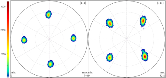
Figure 2. Pole figure along the (111) direction of CeO2 (left) and of Ni–W (right).
Download figure:
Standard image High-resolution imageFigure 3 shows SEM images of a CeO2/Ni–W buffer layer surface after the annealing process in a temperature range relevant for 11 film deposition (>300 °C). The structural and morphological properties of the CeO2 film are unchanged after the annealing, in particular the surface is uniform, smooth and dense. Above all, the CeO2 film assures a good coverage of the grooves among the substrate–grain boundaries. This result shows that CeO2 film on Ni–W is a robust template suitable for the 11 film deposition.
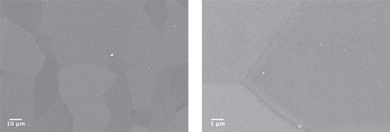
Figure 3. SEM images of the CeO2 film grown on Ni–W after the annealing process in FST deposition relevant conditions.
Download figure:
Standard image High-resolution image3.2. Fe(Se, Te) coated conductors
Figure 4 reports a θ−2θ scan of an FST thin film deposited on the CeO2/Ni–W template. Besides the (001) peaks corresponding to the 11 phase, the peaks coming from the template are clearly visible, but no other peaks are present relative to other orientations or phases, indicating an optimum c-axis alignment of the growth and a high purity of the phase. The ω-scan on the (002) peak, reported in the inset of figure 4, shows a FWHM value Δω of about 6.6° measured in the transverse direction, which is compatible with the value measured in the CeO2 buffer layer (see inset of figure 1) and confirms a good out-of-plane texture.
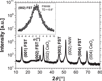
Figure 4. θ−2θ scan of the CC with highlighted the (001) peaks of the template and FST film. In the inset, the rocking curve of the (002) peak of the 11 thin films in the transverse direction.
Download figure:
Standard image High-resolution imageIn order to establish the in-plane epitaxy of the growth, we performed φ scans of the (101) reflections of the 11 films. In figure 5(a), we show the polar figures of an FST thin film along the [101] and the [111] direction, while figure 5(b) reports the φ scans of the (101) peak from the thin film compared with those of the (111) peak of the CeO2 and the Ni–W substrate. The lattice of the 11 thin films is therefore aligned cube-on-cube with the Ni–W substrate and rotated by 45° in the ab plane compared that of the CeO2 buffer layer. Eleven thin films grown on CaF2 single crystals and on RABiTS templates show the same behaviour [7, 16]. In fact, the diagonal of the lattice parameter of CeO2 (and CaF2) is about 3.82 Å (∼5.41/√2), which matches exactly with the a lattice parameter of FST. The average in-plane FWHM ΔφFST is about 4.9°, comparable with ΔφCeO2 which is about 4.7°. Therefore, we can conclude that the 11 thin films grown on CeO2/Ni–W templates possess a good biaxial texturing determined by the texturing of the CeO2 buffer layer. Such results are consistent with the data reported in the literature on IBAD templates [6, 11] and RABiTS with a CeO2/YSZ/Y2O3 buffer layer [17].

Figure 5. (a) Polar figures of 11 thin films made along the (111) direction (left) and along the (101) direction (right); (b) from top to bottom: φ scans of the (101) peak of the FST with FWHM = 4.9°, of the (111) peaks of CeO2 with FWHM = 4.7° and of the (111) peak of Ni–W with FWHM = 5.3°.
Download figure:
Standard image High-resolution imageFigure 6 reports the surface of a patterned FST thin film grown on a CeO2-buffered Ni–W substrate. The surface is uniform and shows an irregular hill-and-valley morphology. Average and rms roughness on a 1 μm2 area are 0.7 nm and 0.9 nm, respectively, slightly larger than what observed for CeO2 films (0.4 and 0.5 nm, for average and rms roughness, respectively). In order to correctly evaluate the thickness of the 11 films, the cross section of the fractured sample was analysed with SEM: as shown in figure 7, the thickness of the film is about 100 nm. Both the CeO2 and 11 films appear compact and continuous along the whole thickness suggesting very high-density layers. No interdiffusion process is detectable at the Fe(Se, Te)/CeO2 interface. The Fe(Se, Te) film shows some longitudinal features that suggest a layered growth mechanism.
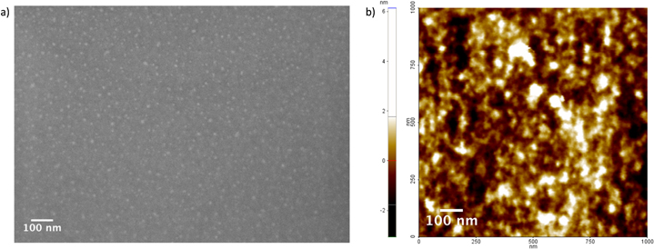
Figure 6. SEM (a) and AFM (b) images of a patterned 11 film grown on a CeO2-buffered Ni–W substrate.
Download figure:
Standard image High-resolution image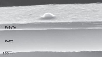
Figure 7. Cross section of the CC analysed with SEM.
Download figure:
Standard image High-resolution imageThe microstructure of the 11 films was investigated by means of the EBSD technique.
Figure 8 shows the EBSD map (a) and the corresponding pole figures (b) of an FST film grown on a CeO2/Ni–W template. In both the EBSD map and pole figures, points are displayed according to the local misorientation angle with respect to the ideal {001}〈010〉 orientation, as shown in the legend of figure 8(c). In addition, grain boundaries above 2° and 10° (thin and thick lines, respectively) are shown.

Figure 8. EBSD map (a) and pole figures (b) of an FST film grown on a CeO2/Ni–W template. The rolling direction is aligned horizontally. Points are displayed depending on their misorientation with respect to the ideal {001}〈010〉 orientation, according to the legend (c). The legend shows the distribution of the acquired points with 1° class width as a function of the misorientation angle from 0° (green) to 20° (red). Points unindexed or above 20° are black. Grain boundaries above 2° (thin line) and 10° (thick line) are included in the map.
Download figure:
Standard image High-resolution imageKikuchi patterns were well fitted using the P4/mmm tetragonal phase and no hexagonal component was detected. As can be seen, the 11 film shows a sharp {001}〈010〉 texture, with a fraction of oriented points of 98.9% within 10°. The film reproduces the microstructure of the underlying Ni–W substrate, as typically observed in RABiTS-based CCs [17]. In fact, the film shows a relative misorientation below 2° in regions of 35 ± 15 μm, which is the typical grain size of a Ni–W RABiT substrate [9, 16–18]. As can be seen, the vast majority of grain boundaries are below 10°. The microstructure is well connected, with the presence of several low-angle grain boundary percolation paths. The critical angle for the existence of a percolative path across the sampled area is 4.5°. This is in line with the value obtained in the case of YBCO films grown on a similar template [19].
The underlying CeO2 buffer layer shows the same microstructure observed in the FST thin film. Figure 9 reports the EBSD map (a) and the corresponding pole figures (b) of the CeO2 film analysed outside the patterned strip used for transport measurements. As can be seen, the CeO2 film shows a strong {001}〈110〉 texture, with a fraction of oriented points of 99.2% within 10°.

Figure 9. EBSD map (a) and pole figures (b) of a CeO2 film grown on a Ni–W substrate, analyzed outside the patterned strip used for transport measurements. The rolling direction is aligned horizontally. Points are displayed depending on their misorientation with respect to the ideal {001}〈110〉 orientation, according to the legend (c). The legend shows the distribution of the acquired points with 1° class width as a function of the misorientation angle from 0° (green) to 20° (red). Points unindexed or above 20° are black. Grain boundaries above 2° (thin line) and 10° (thick line) are included in the map.
Download figure:
Standard image High-resolution imageFrom EBSD microstructural investigation, we can conclude that an epitaxial relationship (001)[010] FST//(001)[110] CeO2//(001)[100] Ni–W has been obtained.
In figure 10 we report the temperature dependence of the normalized resistivity of the 11 CCs up to 18 T in the two directions, perpendicular and parallel to the magnetic field. Tc,0 is about 16 K with an onset above 18 K, comparable with thin films on single crystals or on technological templates [4].
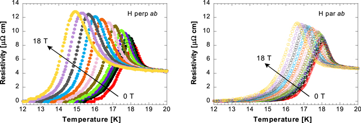
Figure 10. Resistivity as a function of the temperature for the FST thin film measured perpendicular and parallel to the magnetic field from 0 to 18 T (namely at 0, 1, 2, 3, 4, 6, 8, 10, 12, 14, 16, 18 T).
Download figure:
Standard image High-resolution imageAll the plotted ρ(T) curves show low normal state resistivity values and an anomalous bump before the transition with a sharp increase in ρ followed by a steep reduction and then eventually reaching the zero resistance state. The maximum of the bump, Tm, shifts towards lower temperatures coherently with Tc as the applied magnetic field is increased. However, the presence of such a bump was not observed in unpatterned films grown on the same template studied in the present work.
The normal state temperature dependence of the resistivity exhibited by iron chalcogenides is, in general, not trivial. Semiconductor behaviour up to room temperature has been reported in both bulk and films, while a gradual crossover to metallic behaviour is usually observed for temperatures approaching the superconducting transition [20–22]. These features give rise to highly non-linear ρ(T) curves sometimes exhibiting local maxima. A similar bump in the resistivity has been observed in Ba-122/Fe bilayers grown on IBAD tapes with thin Y2O3 buffer layers and was ascribed to the effect of current shunt provided by the metallic template in the presence of a conductive buffer layer [23]. On the other hand, comparable behaviours of resistive transitions have been often reported for different superconducting films and ascribed to a phenomenon related to the current redistribution occurring in presence of sample inhomogeneity, i.e. regions characterized by slightly different Tc and multiple paths for the bias current [24]. Therefore, the present anomalous bump can be explained by invoking the occurrence of a metallic path, likely to be ascribed to a technological issue that arose during the film patterning process, in parallel with the superconducting path with some degree of film inhomogeneity. In particular, the resistive transition behaviour is thus reproduced by equation (1a) of [24], assuming R1 of [24] = metallic path resistance of the present case.
The irreversibility field and the upper critical field values, Hirr and Hc2, are usually evaluated from the R(T, H) curves using, respectively, the 10% and 90% of the superconductive transition criterion. This method is more difficult to be applied to the measurements presented in this work since the reported anomalous behaviour, though accounted for by the presence of multiple paths for the bias current, makes any evaluation of the normal state resistivity value quite speculative. The alternative criterion is thus adopted, considering the 10% of the peak resistance at Tm and Tm(H) dependences as the Hirr and the Hc2 curves, respectively. In the first case, the values will be close to those evaluated with the standard 10% criterion. In the upper critical field case, a qualitative picture of the Hc2(T) dependence can be obtained, even though quantitatively underestimated. The Hc2(T) uncertainty associated with this criterion can be estimated as the temperature interval between Tm and the temperature at which the 50% of the resistance bump is achieved: this means about 0.3 K in self-field increasing to about 0.8 K at 18 T for H perpendicular to the ab planes, while is 0.3 K for any value of H parallel to ab plane.
In figure 11 we report the H versus T diagram, with the upper critical field Hc2 and the irreversibility field Hirr calculated as reported above in both the field directions. Hc2 versus T is very steep near Tc, with a downward curvature and slopes of about 63 T K−1 and 7 T K−1 in the parallel and perpendicular directions, respectively. Such values are quite high, even though not as high as those observed in thin films deposited on single crystals which can reach up to 500 T K−1 and 30 T K−1 in the two directions [25]. The extremely high values reported on our strained film deposited on LaAlO3 and CaF2 were explained in terms of an extreme Pauli-limited Hc2(T), indicative of the Fulde–Ferrell–Larkin–Ovchinnikov state [25]. The slopes near Tc are significantly higher than those reported on IBAD-LaMnO3 (LMO) buffered metal tapes [18]. Trying to estimate Hc2 values at zero temperature, we applied the Werthamer–Helfand–Hohenberg relationship Hc2(0) = −0.693Tc(dHc2/dT)∣Tc and obtained 790 T and 90 T for H//ab and H//c respectively. The anisotropy is not high:  is about 2.3 at 17 K while
  is about 1.8 at 15 K, both higher though than the values reported in thin films grown on single crystals (where Hc2 anisotropy can be as low as 1.2 [16]) and on IBAD-LMO buffered metal tapes [18].
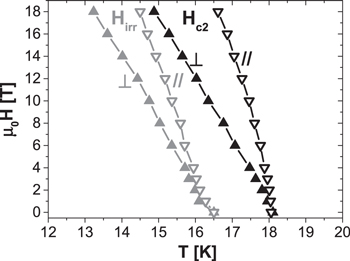
Figure 11. H–T diagram of the 11 thin film. Hc2 and Hirr are calculated from the Tm(H) and the 10% of the peak resistance at Tm dependences, respectively.
Download figure:
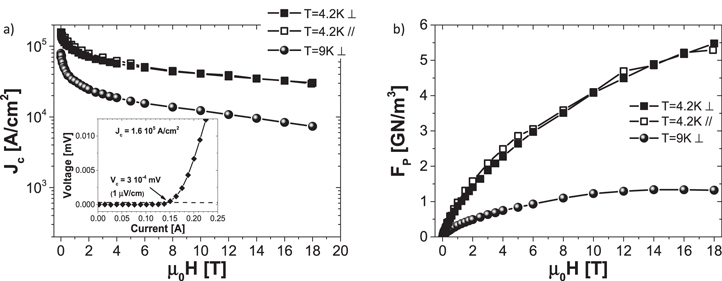
Standard image High-resolution imageIn figure 12(a), we report the critical current density of the CC as a function of the magnetic field measured up to 18 T at 4.2 K and 9 K. The self-field Jc value at 4.2 K is above 1.7 × 10⁵ A cm−2 and above 3.0 × 10⁴ A cm−2 in fields up to 18 T, while the self-field Jc value at 9.0 K is above 7.0 × 10⁴ A cm−2. The Jc curves measured at 4.2 K with H parallel and perpendicular to the tape surface overlap in the whole magnetic field range up to 18 T, indicating an isotropic behaviour in these regimes. In figure 12(b), the pinning force densities calculated as Fp = Jc · B are reported: at 4.2 K we are still far from its maximum at 18 T, while we observe a plateau starting from 14 T at 9 K. The relatively low Jc values with respect to the previously reported FST CC architectures [7, 18] can be explained by the presence of some inhomogeneity in the 11 film. However, this effect can be mitigated through the optimization of growth conditions and texturing of both the buffer layer and FST.
Figure 12. (a) Transport Jc versus H at 4.2 K (both perpendicular and parallel to the magnetic field) and 9 K measured on the strip. In the inset, the I–V curve at 0 T, 4.2 K with an indication of the criterion for the Jc calculation. (b) Pinning force densities, calculated from the critical current density values, as a function of the applied field.
Download figure:
Standard image High-resolution image
4. Conclusions
In this paper we presented the possibility of producing an FST-based CC on a simple RABiTS template made of Ni–W with a CeO2 buffer layer.
The substrate used is a commercial Ni–W tape from Evico, biaxially textured, with a single CeO2 buffer layer, 350 nm thick, deposited through PLD. The Ni–W tape showed in-plane and out-of-plane orientations suitable for 11 thin film deposition, but the optimization of the texturing was obtained with the CeO2 buffer layer which had a misorientation angle both in-plane and out-of-plane lower than the critical angle above which the Jc in the 11 phase starts to decrease exponentially. Moreover, the CeO2 buffer layer acts as a chemical barrier against Ni diffusion which may suppress the superconductivity of FST films.
FST thin films were deposited through PLD on this very simple RABiTS template and showed not only a texturing comparable to the substrates but also superconducting properties comparable to other 11 CCs realized with more complex templates. The superconducting transition occurs at 16 K, and the Jc at 4.2 K is 1.7 × 10⁵ A cm−2 in self-field and above 3.0 × 10⁴ A cm−2 in fields up to 18 T, and can be further improved.
Even if the relatively recently discovered IBS are at a much less mature state of development than other superconducting materials, they have considerable potential for high-field applications. The results shown in this work demonstrate the possibility to produce simple FST-based CCs, making possible the idea of fabricating these kinds of conductors in a cost-effective way for use in large-scale applications.