


Abstract
We have grown an atom-thin, ordered, two-dimensional multi-phase film in situ through germanium molecular beam epitaxy using a gold (111) surface as a substrate. Its growth is similar to the formation of silicene layers on silver (111) templates. One of the phases, forming large domains, as observed in scanning tunneling microscopy, shows a clear, nearly flat, honeycomb structure. Thanks to thorough synchrotron radiation core-level spectroscopy measurements and advanced density functional theory calculations we can identify it as a √3 × √3 R(30°) germanene layer in conjunction with a √7 × √7 R(19.1°) Au(111) supercell, presenting compelling evidence of the synthesis of the germanium-based cousin of graphene on gold.
Export citation and abstract BibTeX RIS

Content from this work may be used under the terms of the Creative Commons Attribution 3.0 licence. Any further distribution of this work must maintain attribution to the author(s) and the title of the work, journal citation and DOI.
Corrections were made to this article on 03 February 2015. A supplementary PDF was added.
Introduction
After the successful synthesis of silicene in 2012, which was followed by a surge of studies on elemental, novel two-dimensional (2D) materials beyond graphene, a daunting quest was to obtain germanene, the germanium-based analogue of graphene, already predicted to possibly exist in 2009. Although its fully hydrogenated form, germanane, was fabricated using a wet chemistry method in 2013, germanene has remained elusive. Here we show compelling experimental and theoretical evidence of its synthesis by dry epitaxial growth on a gold (111) surface.
The discovery of graphene boosted research in nanoscience on 2D materials, especially on elemental ones. In 2012, silicene, graphene's silicon cousin [1], was successfully synthesized on two metallic templates, namely a silver (111) surface [2, 3] and the zirconium diboride (0001) surface of a thin film grown on a silicon (111) substrate [4]. One year later, silicene was also grown on an iridium (111) surface [5]. Germanene, another germanium-based cousin of graphene, along with silicene, had already been predicted to be stable as freestanding novel germanium and silicon 2D allotropes in a low buckled honeycomb geometry by Cahangirov et al in 2009 [6]. In the quest for germanene, its fully hydrogen-terminated partner, germanane (GeH), was first fabricated from the topochemical deintercalation of the layered van der Waals solid calcium digermanide (CaGe2) [7]; next, the stability of germanane was improved by replacing the H atom termination with a methyl group one [8].
Since silicene has, up to now, only been synthesized in dry conditions under ultrahigh vacuum (UHV)—with silver (111) as the favored substrate—trying to synthesize germanene by also growing it on Ag(111) single crystals using germanium molecular beam epitaxy seems tempting. However, to the best of our knowledge, this has failed up to now, because (1) the 'magic mismatch' between three lattice constants of silicene and four of the Ag(111) plane is not fulfilled for germanene, and (2) germanium most probably prefers to form an ordered Ag2Ge surface alloy, where Ge atoms, up to a coverage of one-third of a monolayer (1/3 ML), substitute Ag ones at the silver surface. This surface alloy presents a complex '√3 × √3' structure [9], which not only deviates in its geometry but also in its electronic properties [9, 10] from the simple √3 × √3 reconstruction envisaged earlier [11].
We have thus used a gold (111) substrate instead to avoid such a surface alloy formation. Indeed, for silicene synthesis we deposited silicon on silver (111) surfaces because the inverse system, silver grown on Si(111) surfaces, is well-known to form atomically abrupt interfaces, without intermixing [12]. Our choice of an Au(111) substrate is based on the same strategy. It turns out that among the four noble metals on elemental semiconductor systems studied, namely, Au, Ag/Ge, Si(111) [12], the most similar in several aspects, especially in the growth mode—the Stranski–Krastanov (or layer-plus-islands) mode characterized by the formation of a √3 × √3 R30° superstructure (or wetting layer) associated with the formation of Au trimers on Ge(111) [13] or Ag ones on Si(111)—appeared to be Si/Ag(111) [14] and Ge/Au(111) [15], a trend confirmed in a recent study of Au/Ge(111) [16].
This strategy has paid off. As we show, we have succeeded in growing a 2D germanium sheet with a honeycomb appearance in scanning tunneling microscopy (STM) imaging on top of the Au(111) surface. Its formation shows great similarity to the growth of silicene sheets on the Ag(111) surface [2, 3]. We identify it as a germanene sheet after detailed synchrotron radiation spectroscopy measurements of the deposit (Ge 3d) and substrate (Au 4f) shallow core-levels, and thanks to advanced density functional theory calculations of the geometry and stability of the system, using for the exchange-correlation potentials the general gradient approximation (see the supplementary material, available at stacks.iop.org). Independently, and nearly in parallel, another group has concluded the formation of a germanene layer on a platinum (111) template, but with this appearing strongly distorted, based only on STM observations of a hexagonal arrangement and density functional theory calculations in the basic local density approximation [17].
One can anticipate this new discovery having a major impact because of the expected very high mobilities of the carriers [18]; the potential optical applications [19]; the predicted robust 2D topological insulator character, nearly up to room temperature, resulting from the large effective spin–orbit coupling [20, 21], opening the way to the quantum spin Hall effect [22]; the possibility of very high Tc superconductivity [23, 24]; and, last but not least, the practicability of direct integration in the current electronics industry.
Results and discussion
The methodology we adopted is very similar to the one we used for the synthesis of silicene on Ag(111) (see [2] for details); the silver sample was exchanged for a gold (111) one and the silicon source in the experimental set-up in Marseille was replaced by a germanium evaporator to deposit Ge atoms onto a clean Au(111) surface prepared in a standard fashion by Ar+ ion bombardment and annealing. The in situ cleaned Au(111) surface is characterized by its well-known 22 × √3 herringbone structure [25]. Low energy electron diffraction (LEED) and STM observations were performed at room temperature (RT) at different stages of the growth, carried out at several substrate temperatures to determine potential candidates for germanene in an overall multiphase diagram, as was already the case for silicon deposition onto Ag(111) [26].
In this paper we focus on one of the phases obtained at ∼200 °C growth temperature at about 1 ML coverage, as estimated from the 32% attenuation of the Au 4f7/2 core level intensity. It covers extended regions, larger than 50 × 50 nm2 in size, with a honeycomb appearance and a very small corrugation of just 0.01 nm, as well as with a weak long range modulation in STM imaging, as displayed in figure 1.

Figure 1. (a) 16.2 nm × 16.2 nm STM image of the modulated honeycomb √7 × √7 superstructure with a close-up in the bottom left corner (sample bias: −1.12 V, 1.58 nA; the √7 × √7 unit cell is drawn in black); (b) associated LEED pattern taken at 59 V; (c) schematic illustration of one sixth of the pattern, filled dots: hidden (0,0) spot and integer order spots, open circles: spots corresponding to the √7 × √7 superstructure (in red), the √19 × √19 one (in green) and the 5 × 5 (in blue).
Download figure:
Standard image High-resolution imageHowever, as was the case for the main silicene phase on Ag(111) (denoted 3 × 3/4 × 4 to illustrate the 3 × 3 reconstruction of silicene in a 4 × 4 coincidence cell on Ag(111)), here, again, the observed honeycomb arrangement is too large [2] to correspond directly to a germanene primitive cell. Instead, its cell size fits to a √7 × √7 R(19.1°) superstructure in terms of Au(111), which is in accord with the LEED pattern of figure 1(b). This somewhat astonishing LEED pattern, with many extinctions, reflects the diffraction from three main co-existing phases, as shown schematically in figure 1(c): √19 × √19 R(23.4°), 5 × 5 and √7 × √7 R(19.1°) phases, the last one being of prime interest here, noted with reference to the Au(111)1 × 1 basis vectors. The extra spots observed at a small distance from the integer order ones suggest the presence of a distortion with a long repetition length, most probably reflecting the modulation seen in the STM images, which can be related to underlying remnants of the native herringbone structure of the pristine Au(111) surface. At this stage, we stress that in most circumstances the growth of silicene on Ag(111) also takes place in several phases, the most frequent LEED pattern corresponding in this case to a superposition of diffraction patterns, with many extinctions stemming essentially from √13 × √13 R(13.9°) and 4 × 4 phases (labeled with reference to Ag(111)(1 × 1), but also, typically, a √19 × √19 R(23.4°) phase [26]. Hence, somehow, the astonishing LEED pattern we get for the present Ge/Au(111) system should not be such a surprise.
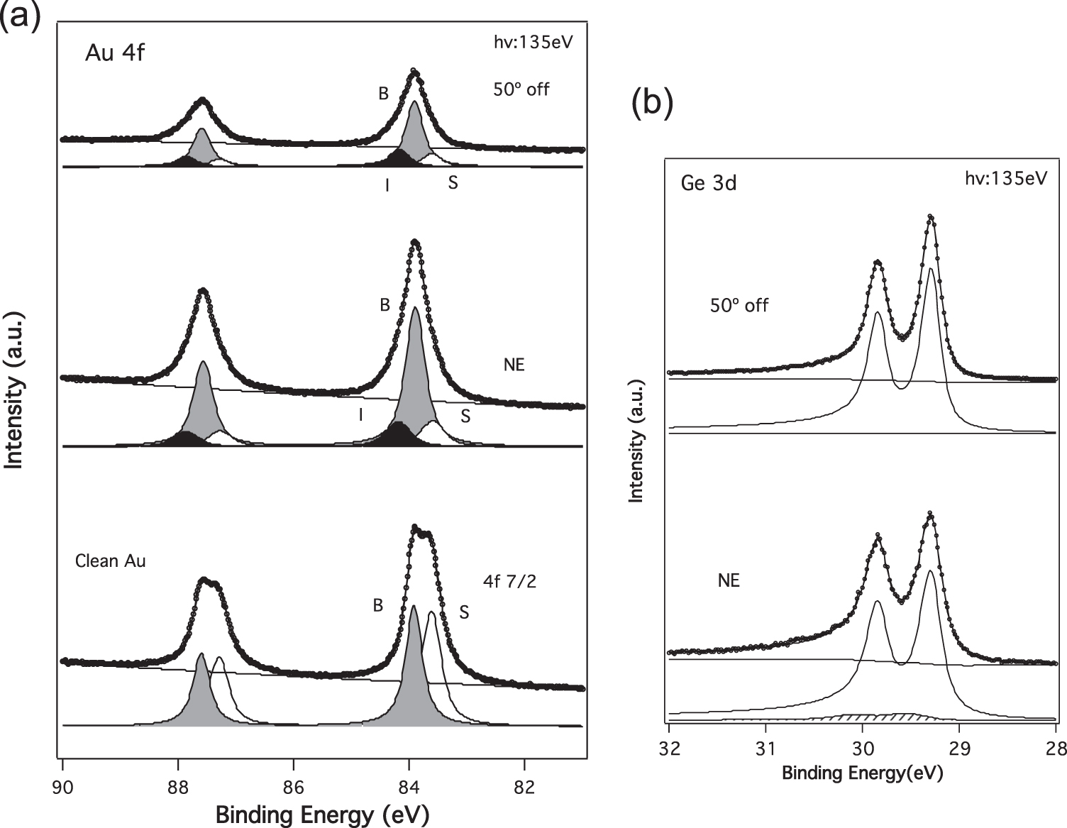
In line with the silicene phases on the Ag(111) surface, the √7 × √7 R(19.1°) superstructure in terms of Au(111) we focus on here could possibly be associated with a 2 × 2 or a √3 × √3 R(30°) germanene phase on top of the Au(111) surface (symmetry, in each case, imposing a two-domain structure). This view is supported by the synchrotron radiation core-level spectroscopy measurements displayed in figure 2 (for details on the data acquisition and fitting procedure and parameters, see the supplementary material).

Figure 2. Synchrotron radiation Au 4 f (a) and Ge 3d (b) core-level spectroscopy measurements at normal (NE) and 50° off-normal emission, taken at hν = 135 eV for the 2D phases of Ge grown on Au(111) at ∼200 °C; B, S and I are bulk, surface and interface components, respectively.
Download figure:
Standard image High-resolution imageThe clean Au(111) 4f core-levels are fitted with bulk (B) and surface-shifted (S) components of similar intensities in the highly surface-sensitive conditions of the measurements (typically, the kinetic energy of the measured Au 4f7/2 line at ∼46 eV corresponds to the minimum of the escape length of around 0.5 nm). After germanium deposition at ∼200 °C and the growth of the two-dimensional phases, as displayed in figure 1, the total Au 4f intensity at normal emission is reduced by ∼32%; still, a fraction of the Au(111) surface (about 25%) remains uncovered since the surface component is not totally quenched. On the high binding energy side a new component, denoted I and representing ∼15% of the total Au 4f intensity, has developed. The relative intensity ratio I/B at normal emission (0.21) increases to 0.29 at 50° off-normal emission, while the S/B ratio barely changes. This indicates that the gold atoms contributing to this I component are at the very top surface. The corresponding Ge 3d core-levels are fitted with a very narrow, asymmetric single component at 50° off-normal emission, in extremely surface sensitive conditions (escape depth estimated at ∼0.4 nm), essentially signaling a unique environment of the germanium atoms at the very top surface and their metallic character; we assign the small broad additional component (just 9% of the total intensity) at normal emission to defect sites. The essentially unique Ge species indicate that no formation of a surface alloy occurs, at variance with the Ag2Ge one formed in the case of Ge deposited on Ag(111) surfaces [9, 11] or the one initially formed upon Ge deposition onto the Au(110) surface [27]. In this respect, we note that the formation of a surface alloy is surface dependent; typically, it takes place upon Ge deposition onto the Ag(111) surface, but not onto the Ag(110) and Ag(100) ones.
Based on these core-level results and the honeycomb appearance of the STM images of figure 1, we can assume that the germanium 2D overlayer grown on top of the Au(111) surface is composed of germanene sheets arranged in either a √19 × √19 R(23.4°) supercell (with reference to Au(111) 1 × 1), a 5 × 5 one or a √7 × √7 R(19.1°) one. As mentioned above, this last supercell could correspond either to a 2 × 2 germanene reconstructed epitaxial sheet (projected in-plane Ge-Ge distance: dGe-Ge = 0.221 nm) or to a √3 × √3 R(30°) one (dGe-Ge = 0.255 nm), since the corresponding value for freestanding germanene is dGe-Ge = 0.238 nm [6], while the √19 × √19 R(23.4°) and 5 × 5 ones could correspond respectively to a 3 × 3 (projected in-plane Ge-Ge distance: dGe-Ge = 0.242 nm) and a √13 × √13 R(13.9°) one (dGe-Ge = 0.231 nm).
In the following we address the question of the epitaxial structures for the √7 × √7 R(19.1°) supercell, since this is the one observed in STM imaging as a honeycomb arrangement. To this end we have undertaken to determine the minimum energy configuration within this supercell through density functional theory calculations, even searching for a surface alloy (although very unlikely from the core-level measurements) and also allowing for possible substitution of few Au atoms within the germanene sheet; for details of the calculations, see the supplementary material.
The lattice mismatch between the cell sizes of 2 × 2 freestanding germanene and those of the √7 × √7 Au (111) surface appears to be small (8.12 Å versus 7.78 Å). However, the 4.2% compression, along with the strong Ge–Au interaction, distorts the germanene lattices and induces considerable buckling in the structure. The atomic structures and simulated STM images of the two lowest energy structures for 2 × 2 germanene on top of the √7 × √7 Au supercell are shown in figures 3(a) and (b). The average height variations in structures 1 and 2 are 0.150 nm and 0.142 nm, respectively, much larger than what is measured in experiments. Therefore, these two structures are not the structures observed in experiments.

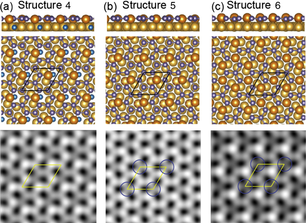
Figure 3. (a)–(c) Atomic structures (side and top views) and simulated STM images of three different models of germanene on the √7 × √7 Au(111) surface. Structures 1 and 2 have 2 × 2 periodicity, while structure 3 has √3 × √3 periodicity with respect to germanene. The protruding Ge atoms are highlighted in dark red. The supercells in the STM images are highlighted with yellow lines. (d) Comparison between the experimental image (left panel, close-up from figure 1(a)) and the simulated STM image for structure 3 after smearing (right panel).
Download figure:
Standard image High-resolution imageOn the other hand, a very flat structure is obtained when √3 × √3 germanene is placed on top of the √7 × √7 Au surface. It corresponds to a coverage ratio θGe = 6/7 = 0.857, typically lower than θSi = 18/16 = 1.125 for the prototypical 3 × 3/4 × 4 silicene on Ag(111), which can be related to the larger size of Ge atoms compared to Si ones, since gold and silver have nearly the same lattice parameter, and also probably points to different interactions with the substrates. The lowest energy structure in this configuration is shown in figure 3(c). The height variations of different Ge atoms are less than 0.05 nm. Compared with the previous two structures, this one has a lower absorption energy, which is defined as:

where EGe/Au(111), EAu(111), and EGe represent the total energies of the germanene-covered Au slab, the pure Au slab and the isolated Ge atom, respectively, and NGe represents the number of Ge atoms in the supercell. As seen in table 1, the absorption energy of this structure is even lower than the bulk cohesive energy of diamond Ge, indicating that it is more energetically favorable to form such a layer structure than to form Ge clusters on the Au(111) surface. This is in contrast to the Ge overlayer formed on top of graphene [28]. In that case, the absorption or binding energy of the Ge overlayer is higher than the cohesive energy of bulk Ge, so, as the size of the Ge cluster becomes larger, 3D growth becomes more energetically favorable. The simulated STM image for structure 3 is shown in figure 3(c). As highlighted with blue circles, there is a darker region for each supercell. With the consideration of the tip effects, an image similar to those observed in experiments may be obtained by Gaussian smearing with width σ = 0.6 Å, as shown in figure 3(d).
Table 1. Absorption energies and core level shifts for different germanene structures on the Au (111) surface. The cohesive energy of bulk germanium in its cubic diamond-type structure is calculated to be −3.727 eV/atom. The main components of the Ge 3d core levels are set to 0.00 eV.
| Energy per Ge atom (eV/atom) | Buckling (Å) | Ge 3d core level shifts (eV) | Au 4 f core level shifts (eV) | |
|---|---|---|---|---|
| Structure 1 | −3.641 | 1.50 | ||
| Structure 2 | −3.648 | 1.42 | ||
| Structure 3 | −3.744 | 0.47 | −0.09, 0.00, 0.06 | 0.15, 0.37 |
| Structure 4 | −3.815 | 0.28 | 0.00, 0.17, 0.34 | 0.24, 0.36, 0.43 |
| Structure 5 | −3.847 | 0.23 | −0.14, 0.00, 0.11 | −0.11, 0.27, 0.33 |
| Structure 6 | −3.868 | 0.41 | ≤0.03 | −0.12, 0.17, 0.22,0.29 |
The Au 4f surface core level shift calculated for a pure seven-layer Au slab is −0.35 eV, which agrees well with the experimental value. The Ge 3d core level shift between different Ge atoms in structure 3 has three components, as shown in table 1, with the energy of the main component set to 0.00 eV. The intensity ratio between these three components is 1:4:1. The difference between each small component and the main component is less than 0.09 eV, which is also consistent with our experimental results. The calculated Au 4f core level shift for the Au atoms below Ge atoms in structure 3 has two components: one is shifted by 0.37 eV and the other is shifted by 0.15 eV, with relative intensity ratio 4:3. These two components, the signals of which are attenuated by the germanene layer above, can be related to the component I, the interface component, located at the left of the bulk peak in experiments.
Although our calculations on structure 3 agree very well with our experiments we would also like to explore the possibility of forming a Ge–Au surface alloy on the Au(111) surface. For example, switching the position of one Ge atom and one Au atom in structure 3, the total energy of the system can be even lower. The lowest energy structure from switching one pair of atoms is shown in figure 4(a). The total energy of this structure ('structure 4') in the √7 × √7 Au supercell is lower than that of structure 3 by 0.43 eV. A larger scale calculation in a 2√7 × 2√7 Au supercell shows that the total energy decreases almost linearly with the increasing number of switching pairs, from one pair up to three pairs. The surface of such a structure is also very flat, with height variations of less than 0.3 Å. The simulated STM image is shown in the bottom panel of figure 4(a). Calculations indicate that the Ge 3d core level spectra should have three components (see table 1). In particular, the two surface components are separated by about 0.17 eV, and the component corresponding to the subsurface Ge atom shifts to 0.34 eV higher than the majority of surface components. The disagreement between the calculation and the experimental results for the Ge 3d core-level indicates that structure 4 is not the one observed in experiments.
Figure 4. Atomic structure (side and top views) and simulated STM images of three different germanene structures having substitutional Au atoms. The Au atoms in the surface layer are highlighted in orange and the Ge atoms in the subsurface layer are highlighted in light blue.
Download figure:
Standard image High-resolution image
When there are only five Ge atoms on the Au(111) surface within the √7 × √7 Au supercell, the relaxation of all the surface layers will result in a structure similar to that shown in figure 4(b), i.e., one Au atom is pulled out of the Au surface and forms a honeycomb lattice with the other Ge atoms, leaving a vacancy in the subsurface (the locations of the vacancy are highlighted with red circles). Following the definition in equation (1), the absorption energy per Ge of this structure is even lower than that of structure 3, by 0.049 eV. However, with a vacancy in the subsurface, this structure is not stable. Other Au atoms will diffuse from the bare surface or from the bulk to fill the vacancy to form a more stable structure. The new structure consists of a honeycomb germanene lattice with some Ge atoms substituted by Au atoms and the original Au surface. The lowest energy structures with one and two Ge atoms substituted by Au atoms are shown in figures 4(b) and (c), with the vacancies in 4(b) filled with Au atoms. However, it is not possible to compare the absorption energy of Ge atoms in structure 3 with that in structure 5, since equation (1) does not apply to the latter. Instead we introduce a new definition for absorption energy of Ge atoms in systems having Au atom substitutions like structure 5:

where  is the number of substituting Au atoms and
  is the cohesive energy per atom of bulk gold. After introducing Au atoms in the honeycomb lattice, the Ge–Au layer is still very flat, with height variations of less than 0.5 Å. The simulated STM images are shown in the lower panels of figures 4(b) and (c). For structure 5, there is a darker region in every supercell. For structure 6, besides a darker region, there is a brighter spot due to the Au atom in each supercell. With proper smearing, images similar to those observed in experiments may be acquired.
To conclude regarding these theoretical results, our density functional theory calculations show that the atomic model composed of a √3 × √3 reconstructed germanene sheet on top of a √7 × √7 Au(111) surface matches the STM observations and the core-level measurements very well, although the germanene layer may possess some gold atom substitutions.
Conclusions
To summarize, a two-dimensional germanium layer, forming several phases, has been grown in situ by dry deposition of germanium onto the Au(111) surface, similarly to the formation of silicene on Ag(111). One of these phases displays a clear honeycomb structure with a very weak corrugation in STM imaging. Detailed core-level spectroscopy measurements along with advanced density functional theory calculations allow us to identify this phase as a √3 × √3 reconstructed germanene layer on top of a √7 × √7 Au(111) surface. Through this we provide compelling evidence for the growth of nearly flat germanene, a synthetic graphene-like germanium allotrope that does not exist in nature.
Acknowledgments
Drs F Cheynis, D Chiappe, A Ranguis and A Resta are warmly acknowledged for their contributions to the measurements. We are grateful to Dr M Radović and Dr R S Dhaka at Swiss Light Source and I Vobornik at the Italian synchrotron radiation source Elettra, whose outstanding efforts made these experiments possible. Funding from the 2D-NANOLATTICES project within the 7th Framework Programme for Research of the European Commission, under FET-Open grant number 270749 is greatly appreciated. We acknowledge support from the European Research Council Advanced Grant DYNamo (ERC-2010-AdG-267374), Grupos Consolidados UPV/EHU del Gobierno Vasco (IT-578-13) and European Commission project CRONOS (grant number 280879-2).