


Abstract
Monolayer (ML) transition metal dichalcogenides (TMDs) are of great research interest due to their potential use in ultrathin electronic and optoelectronic applications. They show promise in new concept devices in spintronics and valleytronics. Here we present a growth study by molecular-beam epitaxy of ML and sub-ML MoSe2, an important member of TMDs, revealing its unique growth characteristics as well as the formation processes of domain boundary (DB) defects. A dramatic effect of growth temperature and post-growth annealing on DB formation is uncovered.
Export citation and abstract BibTeX RIS

Content from this work may be used under the terms of the Creative Commons Attribution 3.0 licence. Any further distribution of this work must maintain attribution to the author(s) and the title of the work, journal citation and DOI.
1. Introduction
The miniaturization of electronic and optoelectronic devices has made two-dimensional (2D) monolayer (ML) materials the forefront of scientific research today [1–3]. New physics and properties have emerged from studies of 2D crystals, and new concept devices have been proposed and demonstrated [2, 4, 5]. Among the various 2D crystals, ML transition metal dichalcogenides (TMDs), such as MoS2, WS2, MoSe2, and WSe2, are attracting particular attention due to their sizable energy bandgaps, strong spin–orbit coupling, and valley-contrasted physics and properties. They show promise for spin and valleytronic device applications [2, 3, 6–8]. Bulk crystals of TMDs consist of stacks of MX2 (M = Mo or W, and X = S or Se) units or MLs held together by the weak van der Waals (vdW) forces along the c-axis direction [9]. Within each MX2 ML, the metal and chalcogen atoms are chemically bonded. Therefore, flakes of ML TMDs are obtainable by exfoliation from bulk crystals using, for example, Scotch tape [10]. Many experiments have been performed on such exfoliated samples for physical properties and for device explorations [2–5, 10]. The desire for large and better quality samples has recently prompted the growth in production of TMD films using chemical vapor deposition (CVD) [8, 11, 12] and molecular beam epitaxy (MBE) [13–15] techniques. Because of the advantages of MBE in epitaxial thickness and doping control, as well as its superiority in heterostructure fabrication, the MBE of ML TMDs has become increasingly popular and attracted more and more attention [13–15]. There are, however, challenges in the MBE growth of TMD films. The vapor pressures between transition metals (Mo and W) and chalcogen elements (S and Se) are very different, making the 'growth window' of the materials narrow and so more stringent deposition conditions are required. The weak vdW interaction between the deposit and the substrate during TMD growth on highly ordered pyrolytic graphite (HOPG) for example, along the c-axis direction makes the system special with some unique growth characteristics, which have been referred to as vdW epitaxy [16–18]. The kinetics of vdW epitaxy, however, remains underexplored.
Here we present a systematic study of the MBE growth of MoSe2, an important member of the TMD family, by in situ surface characterization tools such as reflection high energy electron diffraction (RHEED), low energy electron diffraction (LEED), and scanning tunneling microscopy (STM). Elemental Mo and Se are used as the sources while HOPG and graphene-on-SiC are adopted as the substrates. The surface morphologies of sub-ML MoSe2 are followed and the domain boundary (DB) defects, including their formation process, are examined. We reveal a dramatic temperature effect on DB defect formation in MoSe2. Finally, characterizations by photoluminescence (PL) and Raman spectroscopy of ML MoSe2 films with different defect densities are carried out, showing the effect of DB defects on the properties of the films.
2. Experiments
MBE deposition of MoSe2 was carried out in an Omicron ultra high vacuum (UHV) system with base pressures in the 10−10 mbar range. During growth, the pressure in the MBE chamber was increased to ∼10−7 mbar due to the high Se flux used, which was more than ten times that of Mo. The fluxes of Se and Mo were generated from a dual-filament Knudsen cell and an e-beam cell, respectively, where the cell temperature of the Se source was 120 °C with the 'hot-lip' being at 220 °C to prevent Se condensation at the cell orifice. A Mo rod of diameter 2 mm and of length 5 cm was installed in the e-beam cell operated at 45 W. The flux of Se was estimated to be about 7 × 10¹⁵ atoms cm−2 · h−1 from the beam-equivalent pressure measurement using a beam flux monitor at the sample position. The flux of Mo, on the other hand, was indicated by a built-in flux monitor in the cell and calibrated by the film growth rate (which was limited by the metal flux). The latter was determined by post-growth coverage measurements by the STM, and in this study a constant rate of 0.5 MLs h−1 was adopted. The freshly cleaved HOPG substrate was degassed in a UHV overnight and then flashed at 600 °C prior to MoSe2 deposition. The substrate of graphene-on-SiC was prepared in the UHV chamber by heating the Si-face SiC wafer under the flux of Si [19, 20]. The latter had a better crystallinity than the HOPG, which was found to be essential for achieving high-quality, single-crystalline MoSe2 epifilms. The growth temperature was varied in the range of 200–450 °C. For some samples, post-growth annealing was performed at ≤600 °C for one hour by radiative heating from a set of W filaments at the back side of the sample plate. During both MBE deposition and post-growth annealing, the sample surfaces were monitored by the RHEED operated at 10 keV. Room-temperature (RT) STM and LEED measurements were performed in adjacent UHV chambers, and for the former, a constant current mode of operation was adopted throughout and the tunneling current was 0.1 nA. Raman spectroscopy and PL measurements were performed in ambient atmosphere at RT, using a 633 nm laser and the Renishaw spectrometer.
3. Results and discussions
Crystalline MoSe2 is the stable phase under excess Se. For MBE growth of MoSe2, an overpressure of Se of more than ten times that of Mo has been used throughout this experiment. Such a high Se flux is required not only because of the thermal equilibrium considerations but also because of the kinetics of high rate Se desorption from the surface during MBE. The high surface desorption rate of Se sets an upper limit on the growth temperature. At the growth rate of 0.5 MLs h−1, the temperature is found to be no higher than 500 °C. Nevertheless, a higher temperature (e.g., 580 °C) can be used for annealing without decomposing the film after it is grown.
3.1. Nucleation and epitaxial growth mode of MoSe2 on HOPG and graphene
On HOPG and graphene, MoSe2 growth proceeds over a wide range of growth conditions via the nucleation of 2D islands on the surface. The epitaxial growth mode is layer-by-layer according to the RHEED and STM observations. The RHEED patterns are streaky throughout the deposition process and the STM micrographs reveal the typical terrace-and-step morphology of the surfaces. As an example, figure 1(a) shows the surface of a MoSe2 film, which is 1.4 MLs thick and deposited on HOPG at 390 °C. Despite the variations in film thickness across the sample due to the >1 ML deposit coverage and the kinetics of MBE, the surface appears atomically smooth, revealing ML high islands or steps as exemplified by the line profile in the inset. The RHEED pattern of the sample (also shown in the inset) is streaky, affirming the flat morphology of the film. Inter-diffraction streak spacing is found to match well with a strain-free MoSe2, therefore the film is unstrained despite the lattice misfit with the substrate. In other words, the substrate lattice does not provide a constraint for strained MoSe2 epifilms, a property characteristic of vdW epitaxy [16–18].
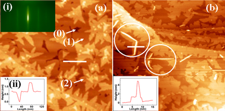
Figure 1. (a) STM image (size: 500 × 500 nm2, sample bias Vsample = −2.5 V) of an MBE-grown MoSe2 film on HOPG at 390 °C for the nominal coverage of 1.4 MLs. The white arrows point to the exposed substrate ('0'), the 1st ('1') and the 2nd ('2') layer of MoSe2, respectively. The inset (i) is the RHEED pattern taken along ![$[11\bar{2}0],$](https://content.cld.iop.org/journals/1367-2630/17/5/053023/revision1/njp513161ieqn1.gif) and inset (ii) shows the line profile along the white line in the main figure. (b) STM image (size: 100 × 100 nm2, sample bias Vsample = 0.8 V) of another MoSe2 sample grown at 250 °C on HOPG, revealing nanorod features on the surface. The inset shows the line profile taken along the white horizontal line in the main figure.
and inset (ii) shows the line profile along the white line in the main figure. (b) STM image (size: 100 × 100 nm2, sample bias Vsample = 0.8 V) of another MoSe2 sample grown at 250 °C on HOPG, revealing nanorod features on the surface. The inset shows the line profile taken along the white horizontal line in the main figure.
Download figure:
Standard image High-resolution imageWhile one might expect the 2D layer-by-layer growth mode of a layered material because it would lead to a diminishing proportion of lateral chemical bonds present at the island edges, such a growth mode for epitaxial MoSe2 on HOPG (and graphene) is not in full agreement with a recent theoretical prediction of TMD growth on graphene [21]. Instead, the three-dimensional (3D) or Volmer–Weber mode has been suggested for TMD deposition on graphene based on adhesion energy considerations. The stronger adhesion between TMD MLs than that between the TMD and graphene favors the Volmer–Weber growth mode [21]. In the same study, however, it has also been suggested that the 2D mode of growth could be achieved on nitrogen-doped or defected graphene due to the enhanced deposit–substrate interaction as facilitated by the defects. Our observation of the 2D growth mode of epitaxial MoSe2 on HOPG and graphene might thus indicate either that our substrates were defected (e.g. containing the Stone–Wales defects) or that other factors existed stabilizing the 2D film. We did not introduce nitrogen doping, so the doping effect could not be relevant here. One factor that might have stabilized the 2D growth of MoSe2 is the kinetics of MBE. As is described in detail in the following text, we find MoSe2 growth on HOPG proceeds by the nucleation of small islands at the step edges on the substrate surface. This growth process may have changed the character of the deposit–substrate interaction and dominates over the otherwise vdW interaction between the two materials on flat interfaces. In a study by Tenne [22], it was shown that free-standing 2D islands or small clusters of TMDs could be unstable against the formation of nanotubes or fullerene-like structures, by which the lateral chemical bonds at the island edges became saturated or diminished. This is similar to C-nanotube or C60 formation out of graphene sheets. Our observations of the 2D growth mode of MoSe2 on HOPG/graphene over a wide range of deposition conditions may thus indicate the presence of kinetic factors suppressing 3D nanostructure formation during the MBE of MoSe2. On the other hand, under certain conditions nanorod features, illustrated in figure 1(b), are indeed observed on the surface of epitaxial MoSe2, seemingly conforming to the results of Tenne [22]. Nevertheless, we wish to point out that the nanorods in figure 1(b) are substrate-supported rather than free-standing. Furthermore, the chemical identity of the nanorods in figure 1(b) is not yet determined to be MoSe2 or some other phases. Lowering the temperature of deposition seems to favor nanostructure formation, which is also at odds with the thermodynamic considerations. Further studies are needed to elucidate the origin of such nanostructures.
Returning to the 2D growth of MoSe2, STM examinations reveal that its growth proceeds via 2D island nucleation at ascending steps of the substrate as exemplified in figure 2(a), depicting the surface of 0.05 ML MoSe2 deposited on HOPG at 250 °C. The low growth temperature would favor the island nucleation mode of growth over the step-flow mode due to reduced adatom diffusion. However, it is noted in figure 2(a) that the large terraces in between the surface steps remain void of MoSe2 islands, suggesting the long diffusion length of adatoms even at 250 °C. This may be explained by the weak vdW interaction between the deposit and the substrate. The long diffusion length leads to step-flow growth characteristics where adatoms are captured by the pre-existing steps on the surface rather than aggregate to form MoSe2 islands on flat terraces. On the other hand, because of the lateral chemical bond at the step edges, adatoms captured by steps would diffuse at slower rates along the steps, making the steps kinetically roughened. By inspecting figure 2(a), however, one notes distinct triangular islands attached to the ascending steps rather than the roughened step edges. Since the C-bonds at the steps of HOPG do not conform to those of MoSe2, the natural lateral bonding of the two materials for a smooth transition from graphene to MoSe2 at the steps is not viable. Thus it is likely that the steps on the substrate merely act as heterogeneous nucleation sites facilitating MoSe2 nucleation and subsequent growth.
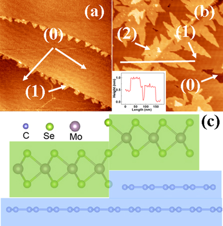
Figure 2. STM images of MBE-grown MoSe2 films on HOPG substrate for (a) 0.05 MLs and (b) 1.4 MLs in coverage. The exposed substrate surface is marked by '0' and that of the deposited MoSe2 by '1' and '2' for the 1st and 2nd layer, respectively. The image size is 400 × 400 nm2 for (a) and 230 × 230 nm2 for (b). The inset in (b) shows the line profile along the white line in the main image. (c) The schematic illustration of the step-facilitated growth process of MoSe2, where MoSe2 islands on the upper terrace (right) nucleate after the growth at the lower terrace (left).
Download figure:
Standard image High-resolution imageThere is an apparent asymmetry in the island population at ascending versus descending steps in figure 2(a), and the nucleation islands appear to heavily populate at ascending steps on the surface (i.e. on the lower terrace of a step rather than on the upper terrace). However, as the deposition continues and the coverage increases, MoSe2 islands become apparent on the upper terrace as well (see figure 2(b)). Line profile measurements across the islands on both terraces show a height difference corresponding to a graphene step. So we suggest the nucleation of MoSe2 on the upper terrace is facilitated by the height difference between ML graphene and ML MoSe2, therefore a new step of the opposite sense is created upon nucleation of the MoSe2 islands on the lower terrace of a graphene step. In other words, an ascending step changes into a descending one and vice versa upon MoSe2 nucleation and growth at the step, promoting continuous growth of MoSe2 on both terraces. This mechanism of growth is schematically illustrated in figure 2(c). Such a growth process obviously results in locally multilayer high films, which is undesirable for obtaining uniform 2D samples. Therefore stepped substrates are less favored for growing high quality 2D crystals of uniform thicknesses.
Another aspect of the morphology in figure 2 is the triangular shape of MoSe2 islands, reflecting the three-fold symmetry of ML MoSe2. Such an island shape suggests a dependence of step energy on crystallographic orientation. Only low energy steps are exposed and bound the islands [23]. For ML MoSe2, the low energy edges may be either Mo- or Se-terminated  steps, which depends also on the possible edge–atom reconstruction and/or chemical saturation [24]. For unsaturated edges without edge–atom reconstruction, Se-terminated ones have a lower energy than that of Mo-terminated steps. Comparing Mo6Se20 (i.e. Se-edged cluster) and Mo10Se12 (Mo-edged cluster) on graphene by density functional theory calculations, we find an ∼70 meV/atom formation energy gain of the former. It is thus likely that the triangular islands are bounded by the Se-terminating steps, and this is consistent with some previous studies [25]. This consideration might also account for the observed triangular island shape of CVD-grown TMD films [8, 12]. For MBE growth, however, there are complications due to the kinetics of adatom attachment/detachment at steps, diffusion across step corners, etc that may also play a role in determining the island shapes [26, 27].
Next we comment on the epitaxial relation between MoSe2 and the substrate. As the HOPG substrate is highly textured in the plane parallel to the surface, epitaxial MoSe2 is similarly textured, preventing us from establishing the exact epitaxial relation, if any, by in situ LEED measurements. Indeed, the LEED patterns taken from such samples usually show a ring feature (figure 3(a)), implying random in-plane rotation domains over the size of the electron beam of the LEED (∼0.2 mm2). On the other hand, as shown in figure 3(b), a selected area (<1 μm2) transmission electron diffraction (TED) pattern obtained using a transmission electron microscope (TEM) (working at 200 keV) clearly indicates crystallography information about the epitaxial relationship between MoSe2 and graphene. Two sets of highly aligned diffraction patterns (from MoSe2 and graphite, respectively) are identified, which are labeled by '(1)' and '(2)' in the figure.

Figure 3. (a), (c) LEED patterns of MBE-grown MoSe2 monolayer on the HOPG (a), and graphene-on-SiC (c), (energy 190 eV). (b) Selective area transmission electron diffraction pattern of a MoSe2 ML on HOPG (energy 200 keV). In all, (1) and (2) label the diffraction features from the substrate and MoSe2 epifilm, respectively.
Download figure:
Standard image High-resolution imageIn order to affirm such an aligned epitaxial relation over larger areas of the sample, we have grown a film on a graphene-on-SiC substrate, where the bilayer graphene film has larger domain sizes. One of the LEED patterns of epitaxial MoSe2 on graphene/SiC is shown in figure 3(c). Clearly, the ring feature of figure 3(a) has broken up into arcs, implying rotation domains of reduced angles (∼20 degrees) over the area of the beam size of the LEED. Notably, these diffraction arcs are aligned with the pattern of the substrate, so setting aside the rotation domains, epitaxial MoSe2 follows the lattice of graphene, i.e. [0001]MoSe2||[0001]graphene and ![${{[10\bar{1}0]}_{{\rm MoSe2}}}$](https://content.cld.iop.org/journals/1367-2630/17/5/053023/revision1/njp513161ieqn3.gif) ||
||![${{[10\bar{1}0]}_{{\rm graphene}}}.$](https://content.cld.iop.org/journals/1367-2630/17/5/053023/revision1/njp513161ieqn4.gif) On the other hand, the six-fold symmetry of the diffraction pattern implies the presence of inversion domains of about equal proportions in the film. The fact that a defined epitaxial relation exists between MoSe2 and graphene suggests non-negligible deposit–substrate interaction at the heterointerface, which marks another characteristic feature of the vdW epitaxy [16–18].
On the other hand, the six-fold symmetry of the diffraction pattern implies the presence of inversion domains of about equal proportions in the film. The fact that a defined epitaxial relation exists between MoSe2 and graphene suggests non-negligible deposit–substrate interaction at the heterointerface, which marks another characteristic feature of the vdW epitaxy [16–18].
STM of samples grown on graphene/SiC and on HOPG showed little difference; because the SiC wafers are highly resistive, STM data of such samples are rather limited for a more comprehensive comparison. On the other hand, as HOPG is conductive, it is better suited for STM studies. We nevertheless expect the two substrates, HOPG and graphene-on-SiC, to behave the same in supporting epitaxial MoSe2 during MBE, as the top surface layer is of the same graphene. Over small areas of the STM measurement (<1 μm2), rotation domains can hardly be detected. In fact, even for samples grown on HOPG, which, according to the LEED, are highly textured, STM images rarely reveal such texturing. This is in agreement with the TED result shown above. The LEED measurements sample much larger areas than STM, so the LEED result can be more representative in revealing the crystallinity of the epifilms. By comparing figures 3(a) and (c), we thus infer that epitaxial MoSe2 on graphene/SiC is superior to that on HOPG.
3.2. Formation of domain boundary defects in epitaxial MoSe2
Inspection of STM images of the MBE-grown films at energies corresponding to the gap region of MoSe2 reveal strikingly bright line features intertwined into triangular networks. An example is shown in figure 4 measured at −1.0 eV relative to the Fermi level (due to unintentional doping, the sample has the Fermi level close to the conduction band minimum). Similar networks of these bright lines in STM images had been reported in the early 1990s and attributed to moiré interference patterns or related effects [28, 29]. Our experiments show that such networks exist not only in MoSe2 on HOPG (graphene) but also on Au(110) substrates [14]. Together with the observation that the density changes with the MBE conditions (see below), we rule out the moiré interference effect. TEM studies of the films establish that the bright lines seen in STM images actually reflect inversion domain boundary (DB) defects, which have given rise to mid-gap electronic states [14]. It is such DB defects that intertwine to form the triangular network. The abundance of DBs, which delineate inversion domains in the film, is consistent with the six-fold symmetry of the LEED and TED patterns as noted earlier. To help to understand the formation process of the DB defects in MBE-grown MoSe2, we carry out deposition experiments at sub-ML coverages and at different temperatures. Figures 5(a)–(c) shows surfaces of a set of samples of different deposit coverages, and figures 6(a)–(c) compares samples prepared at different temperatures. From figures 5(a)–(c), one makes an interesting observation that the DB defects are not born from the start of MoSe2 island nucleation. Rather they form and develop only after some critical coverage of the deposit has been grown. At low coverage (figure 5(a)), few DB defect can be found. The island edges show bright STM contrasts because the edge atoms introduce in-gap electronic states contributing to the STM contrasts [25, 30]. As the deposit coverage increases, isolated lines of defects start to appear in the interior of the island (figure 5(b)). Continuing growth leads to more lines of defects being introduced, which become increasingly denser and regular in distribution at the central region, whereas in regions close to the edges of the islands, they remain relatively sparse (figure 5(c)). These line defects do not seem to be caused by coalescence of the nucleation islands. If they were, a more random distribution of the lines would be expected and their density would not show the dramatic dependence with film coverage.
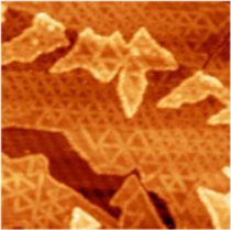
Figure 4. STM image (size: 100 × 100 nm2, Vsample = −1.0 V) of a MBE-grown MoSe2 film on HOPG, revealing a network of bright lines that represent inversion domain boundary defects in film.
Download figure:
Standard image High-resolution image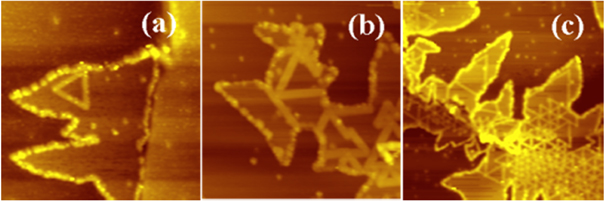
Figure 5. STM images of MBE-grown MoSe2 on HOPG at different coverages. (a) 0.2 MLs. Image size: 80 × 80 nm2, Vsample = −1.0 V. (b) 0.3 MLs. Image size: 50 × 50 nm2, Vsample = −1.0 V. (c) 0.4 MLs. Image size: 100 × 100 nm2, Vsample = −1.0 V.
Download figure:
Standard image High-resolution image
Figure 6. (a), (b) STM images (size: 50 × 50 nm2, sample bias Vsample = −0.8 V) of MBE-grown MoSe2 films on HOPG at different temperatures as marked. (c) STM image of a sample grown at the same temperature as for (a) but underwent annealing at 580 °C for 1 h (size: 500 × 500 nm2, sample bias Vsample = 0.7 V).
Download figure:
Standard image High-resolution imageFormation of the DBs in crystalline films can be energetically costly and their nucleation is usually the response of a film to stress. For epitaxial MoSe2 on HOPG along the c-axis, the hetero-interface is of weak vdW bonding and can barely sustain large lattice misfit strain. As noted earlier, epitaxial MoSe2 is strain-free even at the very early stage of deposition. Another source of stress is thermal, which is inevitably introduced during temperature ramping after film growth. We have examined the relevance of thermal stress by varying the ramping rate of the substrate temperature but observed little effect. However, as shown in figures 6(a) and (b), the temperature used during MoSe2 deposition does affect the defect density—the higher the temperature, the lower the density. Even more dramatic is post-growth annealing, and we find that the DBs may be completely annealed out at high temperatures as exemplified in figure 6(c).
The DB formation in epitaxial MoSe2 appears kinetic driven. Upon high temperature annealing whereby the sample becomes DB-free, bringing the sample back to the growth temperature does not seem to reintroduce the defects. Annealing under different environments, e.g. in vacuum or in Se over-pressure, shows a noticeable difference in the diminishing rate of defects: they anneal out faster under Se flux than in vacuum. Moreover, as-grown WSe2 films do not show similar networks of DBs despite similar MBE conditions [31]. These findings may help to identify the reason and mechanism of DB formation in MBE MoSe2.
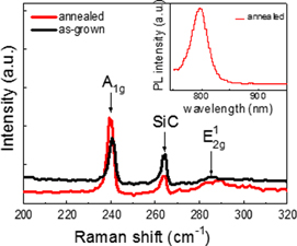
Lastly we show that DB defects significantly affect the optical properties of the materials. Because the conductive HOPG substrate effectively quenches the photoluminescence of the sample, and the epifilms are also textured on HOPG (see figure 3), we compare the optical properties of samples grown on graphene/SiC in the following text. While films that have undergone the annealing procedure clearly show direct band-edge PL emission at 800 nm (see figure 7 inset), those without annealing do not show clear band-edge luminescence due to the high density of non-radiative defects in the film. Raman spectroscopy measurements reveal a wavenumber shift of the A1g, out-of-plane, vibration mode between samples with versus without DB defects. Figure 7 (main panel) compares two spectra from ML MoSe2 grown on graphene/SiC containing, respectively, (i) high and (ii) low density of DB defects due to annealing or not. In the spectra, the vibrational modes of SiC and epitaxial MoSe2 are all identified, and the peak at 239.6 cm−1 in (ii) (red) and at 240.6 cm−1 in (i) (black) corresponds to the A1g mode of MoSe2. There is an obvious wavenumber shift by ∼1 cm−1, which may reflect a difference of interaction strength at the film–substrate interface. As spectrum (i) is for a sample containing a high density of DB defects and its Raman peak is at a higher frequency, implying enhancement of the hetero-interface interaction, it is likely that the defects contribute to the strengthening of the deposit–substrate interaction.
Figure 7. Raman spectra of ML MoSe2 epifilms grown on graphene/SiC with different defect densities. Spectrum (i) in black color is for an as-grown sample with high DB density, and (ii) in red color is for a sample that underwent high temperature annealing and thus has a low density of defects. The vibrational modes of SiC and MoSe2 are marked. Note the peak position shift between (i) and (ii) of the A1g mode from MoSe2. Inset: room-temperature PL spectrum from an annealed MoSe2 film grown on graphene/ SiC.
Download figure:
Standard image High-resolution image
4. Summary
In summary, MBE growth of MoSe2 on HOPG and graphene has been studied, and the 2D layer-by-layer growth mode has been identified over a wide range of MBE conditions. Step edges of the substrate can act as the mediation sites facilitating MoSe2 growth. An aligned epitaxial relation between MoSe2 and graphene is established, suggesting a non-negligible deposit–substrate interaction in the system. In as-grown MoSe2 epifilms, networks of DB defects exist, the nucleation and development of which depend on film coverage, growth temperature and annealing procedure. High temperature annealing of the sample effectively suppresses the defects. The network of the DB defects is found to enhance the deposit–substrate interaction from Raman spectroscopy measurements. In order to meet the demands of different applications (e.g. electronic versus catalytic), one is able to tune the defect density by adopting different growth procedures and the MBE conditions, making the MBE attractive for fabricating MoSe2 films.
Acknowledgments
We acknowledge the supported of the CRF grant (No. HKU9/CRF/13G) from the Research Grant Council of Hong Kong Special Administrative Region, China. HJL and MHX also acknowledge the support of the internal funds of The University of Hong Kong.