

Abstract
We present a method for few-layer graphene growth on nonmetallic substrates using excimer KrF laser ablation of ordered pyrolytic graphite. The graphene is scalable and its thickness is controllable. It can be deposited on virtually any nonmetallic substrates at a relative low temperature of 750 °C. This laser-based method is highly efficient and the whole growing process takes less than 100 s. Raman spectroscopy confirms the formation of sp2-bonded carbon with a grain size of about 40 nm. The optical transmittance and conductivity of the graphene films are comparable with exfoliated or metal-catalyzed graphene. This work demonstrates a promising laser-based, transfer-free technique for synthesis of graphene.
Export citation and abstract BibTeX RIS
1. Introduction
Graphene, a monolayer of sp2-bonded carbon atoms, is a quasi-two-dimensional (2D) material. It has gained tremendous scientific research interest due to some unique properties, such as giant electron mobility [1, 2], a tunable band gap [3], extraordinary elasticity [4], and typical saturable absorption behavior [5]. To date, many approaches have been developed for the synthesis of graphene, including mechanical cleavage of graphite crystals [1], chemical exfoliation of graphite oxide [6, 7], epitaxial growth on SiC at 1500–1600 °C [8, 9], or chemical vapour deposition (CVD) growth on metals at ~1000 °C [10, 11]. However, while the mechanical method produces high quality graphene flakes, the size of graphene films is limited to small sizes (usually ≪ 1000 μm2). It is not suitable at the moment for scaling and industrial production. Though large area graphene can be achieved on SiC, SiC is very expensive and only suitable for some electronic devices. The CVD method can also yield large-scale graphene on some transition metals, but complicated and skilled techniques have to be employed to transfer the graphene to the required substrate for use in practical electronic devices [10–12]. Today, it is still a challenge to directly synthesize large area graphene on dielectric substrates. Recently, some new methods have been proposed to use a pulsed laser to fabricate graphene on metal substrates [13–15], some nonmetal substrates [16–19], and in liquid nitrogen [20]. Though laser-induced graphenes have a high level of defects, these fabrication ways greatly encourage us to try to grow graphene using laser technology.
In this work, we demonstrated the metal-free synthesis of large area graphene film at a relatively low temperature of 750 °C by using ultraviolet laser ablation of a highly ordered pyrolytic graphite target. The graphene layers can be controlled by altering the laser ablation time. As a unique physical vapor deposition method, this work avoids complex and skilled transfer processes and represents a way forward in the graphene fabrication field.
2. Experimental details
Graphene films were fabricated by pulsed laser ablation of an ordered pyrolytic graphite target using an excimer KrF laser (λ = 248 nm, pulse width = 25 ns, repetition rate = 5 Hz). The experimental setup for graphene growth is shown in figure 1. It consists of two major components: one is an external laser source and another is a stainless steal vacuum chamber. Inside the chamber, a target and a substrate holder are aligned on the same line with a distance of 5 cm. When the incident laser beam bombards the rotating target, the high-energy laser causes localized vaporization of the material, forming energetic carbon species. These carbon species subsequently fly toward the substrate and finally evolve into graphene film. In this experiment, many substrates were used, such as quartz, sapphire and n-silicon substrates. Prior to the deposition, these substrates were cleaned ultrasonically in deionized water and isopropyl alcohol. The deposition chamber was evacuated to a base pressure of less than 10–5 Pa and the films were grown in 10 Pa high purity (5N) argon gas. The typical graphene growth was carried out using laser fluence of 4 J cm − 2, laser ablation time of 90 s and substrate temperature of 750 °C. In order to investigate the growth mechanism, these parameters were tuned accordingly. The rotating target ensured uniform ablation of target and the rotating substrate holder ensured uniform deposition of the films. The thickness and crystalline structure of the graphene were characterized using a Raman Spectrometer (Horiba HR-800) with excitation laser at 532 nm, and high-resolution transmission electron microscopy (HRTEM,JEOL JEM-2100) operated at 200 kV. The transmittances of the graphene films were measured using a spectrophotometer (Hitachi U-4000), where a bare quartz substrate was used as a reference. The electrical measurement of the film was performed using the four-probe method (Keithley 2000 multimeter).

Figure 1. Experimental setup for graphene growth.
Download figure:
Standard image High-resolution image3. Results and discussions
Figure 2(a) shows the Raman spectra of graphene films grown with typical conditions on quartz, sapphire, and silicon substrate, respectively. The well-defined Raman peaks differentiate our thin films from amorphous C (α-C). Typically, the Raman spectrum of α-C has very broad bands enveloping G and D bands, and the 2D band is absent [21]. The G band centered at ~1590 cm − 1 and the 2D band at ~2700 cm − 1 are well resolved, which are the signature of formation of a hexagonal graphitic lattice [22]. The G band is due to first order Raman scattering involving the in-plane E2g phonon at the center of the Brillouin zone. The symmetric 2D band is the result of a second-order process involving two phonons with opposite momentum [23, 24]. The D band (~1350 cm − 1) is due to the out-of-plane breathing mode of the sp2 atoms and only gets activated in the presence of the defects [23]. In the Raman spectra, the D bands were obviously observed, suggesting the existence of defects. Also, a high-order combination of the D and G (G + D) bands at 2930 cm − 1 are visible. Raman spectra obtained from films grown on different substrates are similar. This result is very interesting by considering the fact that the ratio of intensities of the G and 2D bands generally shows a strong dependence on doping [25, 26]. In our case, due to the energetic graphite ablation process, we cannot exclude the presence of trapped charge on the graphene during the growing process. However, because of the identical growing conditions, this unintentional doping could reasonably have similar concentrations and thus equally affect the Raman spectra. In order to evaluate the uniformity of graphene, we also did statistical analysis by Raman map. Figures 2(b), (c) show Raman mapping of the intensity ratio of I2D/IG and ID/IG for a sample grown on a quartz substrate over a 30 × 30 μm area. These maps show the uniformity of this material, and an average value of I2D/IG is ~0.5, indicative of mutilayer grapheme [12, 27]. The quality of graphene and the degree of disorder can be roughly estimated based on the formula La(nm) = 2.4 × 10 − 10 × λ4 × (ID/IG) − 1 [28]. In this measurement, the excitation wavelength λ is 532 nm and the average value of the ID/IG ratio is ~0.5. The average distance between defects is thus estimated to be ~38 nm.

Figure 2. (a) Raman spectra of graphene films on quartz, sapphire, and silicon substrate. Raman mapping of the graphene sample on quartz over a 30 × 30 μm area. (b) I2D/IG and (c) ID/IG.
Download figure:
Standard image High-resolution imageThe crystalline structure of graphene film grown with typical conditions was investigated using HRTEM by transferring it to a small holey copper grid. In order to obtain TEM samples, polymethyl methacrylate solution (PMMA, 20 mg ml − 1) was spin-coated on the graphene/quartz substrate at 4000 rpm for 30 s and dried in air. HF solution (35% in water) was used to etch the quartz substrate, and the PMMA/graphene film was floated on the surface of the solution. The PMMA/graphene film was moved to distilled water several times to rinse the etchant residue. The distilled water was pulled out with a syringe to lower the film onto the copper grid while positioning the film with a needle. Finally, the PMMA was removed in a furnace at 400 °C with Ar (~500 sccm) and H2 (~500 sccm) for ~2 h. Figure 3(a) shows the bright-field HRTEM image of the graphene film. The film is found to be flat and continuous and can be suspended on the grid, indicative of a good mechanical property. To confirm the exact layer number of the samples, we observed their folded regions by using an electron beam parallel to them. The folded regions exhibit two or three dark lines (figure 3(b)), suggesting bilayer or trilayer grapheme [29]. Many folded regions were studied at various positions on graphene sheets. More regions show two dark lines, and about one third of examined regions show three dark lines. For all the examined regions, a monolayer structure (i.e. one dark line image) was not observed. These observations indicated that bilayer structure is predominant in this sample. The typical six-fold symmetry patterns of graphene are observed by selected-area electron diffraction (SAED) from almost every place in the sample as shown in figure 3(c). However, we notice that if the electron beam is moved over a distance of a few nanometers, or if the beam spot is bigger than ~40 nm, two sets of the diffraction pattern like in figure 3(d) are observed. The mixed graphene signals imply that the beam just covers at the grain boundaries [30, 31], indicating that the grain size is ~40 nm.
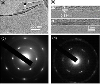
Figure 3. (a) Bright-field HRTEM image of graphene film. (b) HRTEM images of folded edges for bilayer and trilayer graphene. (c) A diffraction six-fold symmetry pattern of graphene. (d) A diffraction pattern from the grain boundaries.
Download figure:
Standard image High-resolution imageLaser-fabricated graphene also shows high transmittance and conductivity. Figure 4(a) shows the transmittances of graphene with different laser ablation time. The transmittance of the graphene can be described as T = T0 (1 − α)n, where T0, n, α are the initial transmittance of the substrate, the number of the graphene layers, the absorption coefficient of monolayer graphene (2.3% at 550 nm), respectively [32, 33]. The bare quartz was used as reference, here T0 = 1. So, the number of graphene layers can be estimated based on the measured transmittance. We study 60 points on the sample grown with typical conditions (ablation time of 90 s). A total of 42 points show a transmittance of ~95% (corresponding to 2 graphene layers), and the other 18 points show a transmittance of ~93% (corresponding to 3 graphene layers). This result demonstrates that about two thirds of the examined regions were bilayer graphene, which agrees well with the HRTEM images. For the samples grown with a lesser ablation time of 30 or 60 s, its transmittance is ~95% or ~100%, indicting that some of the examined regions were covered by bilayer graphene and on the other regions the graphene was not formed. For the sample grown with a greater ablation time of 120 s, its transmittance stabilizes around 91%, reflecting 4 graphene layers. The sheet resistance (Rs) was measured by a four-point method. Figure 4(b) shows the Rs as a function of laser ablation time. The Rs decrease rapidly with the increase of laser ablation time. When the laser ablation time reaches 90 s, the graphene with 2–3 layers shows a Rs of ~1000 Ω ϒ − 1, which is comparable to that of metal-catalyzed grapheme [34]. The high transmittance and low resistance of the films make them ideal material for transparent electrodes. As both transmittance and resistance decrease with the number of layers, we can tune transmittance and conductivity by controlling the graphene layers.
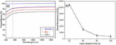
Figure 4. (a) Transmittance spectra of graphene films on quartz, where a bare quartz substrate was used as a reference. (b) The Rs as a function of laser ablation time.
Download figure:
Standard image High-resolution imageIn this work, the growth mechanism of graphene on nonmetallic substrates appears to be very different from the metal-catalyzed CVD growth process [10] or epitaxial growth on SiC [9]. The ordered pyrolytic graphite target has a layered structure and the C-C bond energy is 3.7 eV. The KrF laser has a wavelength of 248 nm, corresponding to a photon energy of 5 eV. So, with each laser shot at 5 eV, the graphitic bonds are rapidly broken by photoelectronic excitation [35], resulting in energetic carbon atoms deposited on the required substrate. According to the previous reports, carbon atoms can form nanographene even at low temperatures of 325–400 °C without the use of metal catalysts [36, 37]. Therefore, it is reasonable that the carbon atoms recrystallize on the high-temperature substrate and evolve into crystalline graphene. In this process, substrate temperature plays a critical role in graphene growth. As Raman spectra in figure 5(a), with substrate temperature decrease from 750 to 150 °C, the intensity ratio of I2D/IG rapidly decreases and ID/IG sharply increases, indicating a big increase of defects [28]. For the substrate temperature at 150 °C, the D and G bands of graphene films merge with each other and evolve to a large broad band, implying the formation of disordered amorphous C [21]. Thus, graphene growth can be understood as a dynamic process with several reaction pathways depending on the details of the environment. At low temperature, most of the carbon atoms do not have enough energy to arrive at an energetically-optimized location before forming a covalent bond. This leads to the formation of bonds along random directions, resulting in small randomly-aligned graphene nanocrystals or even disordered amorphous C at lower temperature. Conversely, at higher temperature, carbon atoms are more active and have higher probability to find the optimized location. Thus these atoms can bond on a larger graphene edge and evolve to graphene film with larger grain size and fewer defects.

Figure 5. Raman spectra of samples with different substrate temperature (a) laser influence (b), and laser ablation time (c).
Download figure:
Standard image High-resolution image
Moreover, the laser fluence is also an important factor in the graphene formation process. As shown in figure 5(b), using 2 and 4 J cm − 2 yielded similar results, while using 6 or 8 J cm − 2 produced a high defect-related D band. In the laser ablation process, higher laser fluence would give rise to more energetic carbon atoms and subsequently lead to violent collisions on the substrate and thus result in more defects [13]. Therefore, it is also important to choose a moderate laser fluence in the graphene growth process. In this growth model, the graphene thickness can be easily controlled by adjusting laser ablation time. Figure 5(c) shows the Raman spectra of the samples with a laser ablation time of 120, 90, 60, and 30 s, respectively. With the decrease of laser ablation time, the intensity ratio of I2D/IG significantly increases, which indicates the reduction of graphene thickness [10]. For the laser ablation time of 30 s, the detected graphene signal was very weak and the Rs was over 10 kΩ ϒ − 1(figure 4(b)), indicating that the continuous graphene film was not well formed due to the lack of carbon source.
4. Conclusions
We have directly fabricated graphene films on different substrates using a KrF excimer laser ablation of an ordered pyrolytic graphite target without the need for a catalytic layer. The number of graphene layers can be controlled to 2–3 layers by adjusting laser ablation time, laser fluence, and substrate temperature. The graphene shows high transmittance and low resistance, demonstrating a promising transfer-free technique for transparent electrode. We demonstrated the formation of large-area graphene with the absence of a catalytic by using a laser technique at relatively lower temperature.
Acknowledgments
This work was supported by the National Natural Science Foundation of China (11274204, 61205174, 61307120, 61377043), Shandong Excellent Young Scientist Research Award Fund (BS2012CL034, BS2013CL011) and Graduate Innovation Fund (BCX1203).