
Abstract
Gallium oxide (Ga2O3), a typical ultra wide bandgap semiconductor, with a bandgap of ∼ 4.9 eV, critical breakdown field of 8 MV/cm, and Baliga's figure of merit of 3444, is promising to be used in high-power and high-voltage devices. Recently, a keen interest in employing Ga2O3 in power devices has been aroused. Many researches have verified that Ga2O3 is an ideal candidate for fabricating power devices. In this review, we summarized the recent progress of field-effect transistors (FETs) and Schottky barrier diodes (SBDs) based on Ga2O3, which may provide a guideline for Ga2O3 to be preferably used in power devices fabrication.
Export citation and abstract BibTeX RIS
1. Introduction
Silicon-based power electronic devices have governed the market for a long time, however it is hard to satisfy the multitude of application requirements nowadays. Wide bandgap semiconductors (bandgap > 3 eV), such as SiC, GaN, ZnO, Ga2O3, and diamond, possess attractive characteristics and are potential candidates for power device applications. These wide bandgap semiconductors have larger bandgaps (Eg) and higher breakdown fields (Ebr) than silicon and provide a gratifying prospect for overcoming the limitations of silicon-based power devices.[1–6] Moreover, as transparent conductive oxides (TCOs),[7,8] these wide bandgap semiconductors can also be used as thin film transistors (TFTs) channel layers[1,2] as well as in flexible integrated circuits (ICs). In response to the social and technological appeal, many efforts have been made to investigate SiC, GaN, ZnO, and relevant semiconductor materials based power devices.
Gallium oxide (Ga2O3), one of the wide bandgap semiconductors, has phases of α, β, γ, δ, and ε,[9,10] an Eg of 4.5–4.9 eV that is larger than those of 4H-SiC (3.3 eV) and GaN (3.4 eV),[11] and an Ebr of 6–8 MV/cm.[12,13] The β-Ga2O3 is the most chemically and thermally stable phase among the five phases,[9,14] and has been widely employed in UV solar-blind detectors,[15–20] UV sensors,[21–23] light emitting diodes (LED),[24] and resistance random access memory (RRAM).[25–28] Baliga's figure of merit (BFOM), a key parameter to evaluate how suitable semiconductor materials are for power device fabrications,[29,30] is as high as 2000–3000, which is many times higher than those of SiC and GaN. The Ga2O3 bulk single crystal can be easily grown by the floating zone (FZ), edge defined film fed (EFG), and Czochralski methods. These techniques have been used to manufacture sapphire substrates for many years, which is a key factor that gives Ga2O3 the big advantages of low cost and mass production.[31–34] As illustrated in Fig. 1(a), Ga2O3 can endure the highest power, surpassing those of the other contrastive materials. Figure 1(b) shows the bandgap-dependent breakdown fields of some semiconductors, and the breakdown field of Ga2O3 is only lower than that of diamond and AlN.
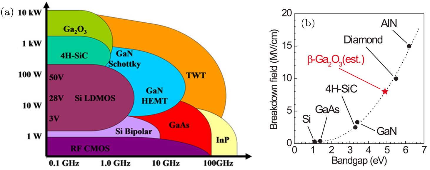
Fig. 1. (a) Power–frequency diagram of application space for several semiconductor materials. Reproduced from Ref. [5]. Copyright 2017, Electrochemical Society. (b) Bandgap-dependent breakdown field. Reproduced with permission from Ref. [11]. Copyright 2012, AIP Publishing.
Download figure:
Standard imageHigh power devices are in great demand in defense and military market. Fortunately, a 2-inch Ga2O3 wafer is available commercially, and 4/6-inch wafers are under development, which will speed the development of Ga2O3 devices. The EFG-grown wafers with various sizes are shown in Fig. 2.

Fig. 2. Status of EFG-grown bulk Ga2O3 wafer sizes. Reproduced from Ref. [5]. Copyright 2017, Electrochemical Society.
Download figure:
Standard imageIn Table 1, the characteristics of Ga2O3, Si, SiC, and GaN are summarized. These materials have been studied extensively in the field of electronic devices. The Eg and Ebr of Ga2O3 are larger than those of the others. The Ga2O3's BFOM is extremely high compared with the Si's BFOM that is taken to be unity, indicating that Ga2O3 has the huge advance in power electronic device applications. Self-heating effects caused by the low thermal conductivity of Ga2O3 can be remitted by using high thermal conductivity substrates instead of homogenous substrates and pulsed modulations (details will be discussed below).
Table 1. Characteristics of Ga2O3 compared with those of Si, 4H-SiC, and GaN.
| Si | 4H-SiC | GaN | Ga2O3 | |
|---|---|---|---|---|
| Bandgap Eg/eV | 1.12 | 3.25 | 3.4 | 4.5–4.9 |
| Dielectric constant k | 11.8 | 9.7 | 9 | 10 |
| Breakdown field Ebr/(MV/cm) | 0.3 | 2.5 | 3.3 | 8 |
| Thermal conductivity λ/(W/cm·K) | 1.5 | 4.9 | 2.3 | 0.25 |
| Electron mobility μ/(cm2/V·s) | 1500 | 1000 | 1250 | 300 |
BFOM  |
1 | 317.1 | 846 | 3444 |
In this review, we summarize recent advances in Ga2O3-based power devices, including field-effect transistors (FETs) and Schottky barrier diodes (SBDs), which are the two typical devices in power electronics.[35] The Ga2O3 based FETs can be categorized into three types, i.e., top-gated metal–semiconductor field-effect transistor (MESFET), top-gated metal–oxide(insulator)–semiconductor field-effect transistor (MOSFET or MISFET), and back-gated FET in Section 2. Ga2O3 based SBDs are illustrated by various metals contacted to Ga2O3 in the following section.
2. Field-effect transistor
In 2005, Chang et al.[36] used molecule beam epitaxy (MBE)[37] to fabricate p-type Zn-doped β-Ga2O3 nanowire-based FET, but the results were not as good as expected, because the drain current was only slightly modulated by the gate voltage. In 2006, Matsuzaki et al. deposited Sn-doped epitaxial Ga2O3 films on a sapphire substrate, and used 180 nm Al2O3 film as the top-gate dielectric layer; the fabricated transistor, with a low drain on/off current ratio (Ion/Ioff) of ∼ 20, could be turned on at a bias voltage of −6.7 V.[38,39] These characteristics were all far from the level required by practical applications. But enthusiasm to study Ga2O3 based FETs was motivated. Since 2012, Ga2O3, especially its power device, has been extensively investigated.
2.1. Top-gated MESFET
In 2012, Higashiwaki et al. fabricated a MESFET by depositing a Sn-doped β-Ga2O3 homo-epitaxial thin film on Mg-doped β-Ga2O3 substrate,[11] the characteristics of the device (shown in Fig. 3) appealing at the practical application level were realized by the advantage of the bandgap of Ga2O3. The breakdown voltage (Vbr) was 257 V, the source–drain spacing (LSD) and the gate-to-drain distance (LGD) were 20 μm and 8 μm, respectively, so the calculated Ebr was ∼ 0.3 MV/cm.
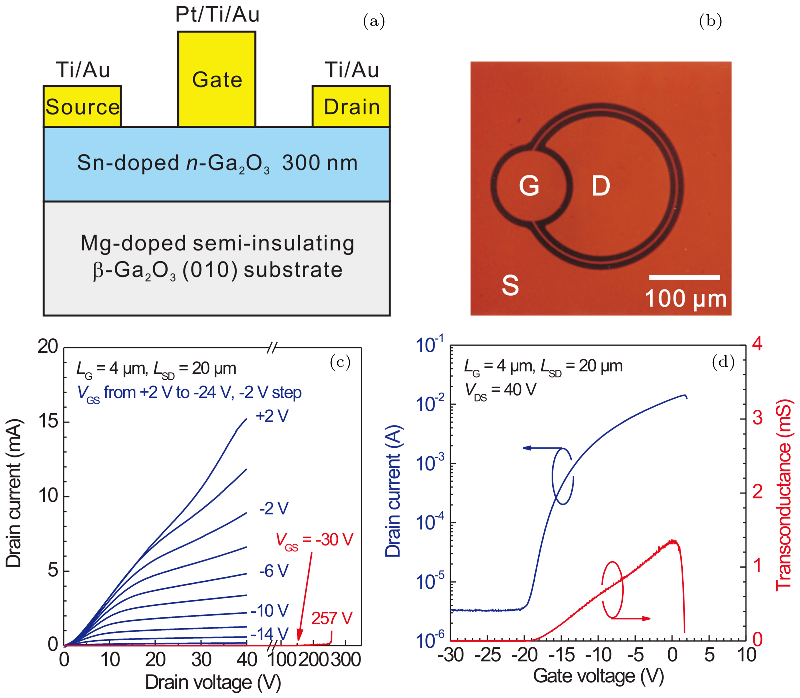
Fig. 3. Sn-doped n-channel MESFETs: (a) cross-sectional schematic, (b) optical microscope micrograph, (c) direct current (DC) output characteristics, and (d) transfer characteristics. Reproduced with permission from Ref. [11]. Copyright 2012, AIP Publishing.
Download figure:
Standard imageDang et al.[40] fabricated a MESFET on a c-sapphire substrate by using Sn-doped α-Ga2O3 thin film grown through the mist-CVD,[41] in which an AgOx Schottky diode was used as the gate. The drain on/off current ratio was about 2 × 10⁷, showing a good switching property. But the breakdown voltage Vbr = 48 V at VGS = −10 V, was lower than that of most reported Ga2O3 based FETs.
The MESFET based on Si δ-doped β-Ga2O3 thin film was fabricated by Xia et al.[42] and McGlone et al.[43] In 2018, Xia et al. obtained an Ion/Ioff up to 105, the Vbr and Ebr of 170 V (LGD = 1.3 μm) and 1.3 MV/cm, respectively.[42] The device was fabricated on a Fe-doped (010) β-Ga2O3 substrate, and a 100-nm unintentionally-doped (UID) buffer layer was deposited on the substrate which contributed to a high drain current density of 140 mA/mm at VGS = 2 V and VDS = 10 V. In the source and drain regions, a regrowth process was performed in order to reduce the contact resistance, then the patterns were finished by i-line (UV, wavelength ∼ 365 nm) photolithography and CF4 inductively coupled plasma reactive ion etching (ICP-RIE). By the same growth and processing method as that shown in Ref. [42], McGlone et al. investigated the trapping effects in a Si δ-doped β-Ga2O3 MESFET with double-pulsed I–V and constant drain current deep level transient spectroscopy measurements.[43] The traps of carriers could affect the device performances, such as the threshold voltage, on-state resistance, gate leakage, and carrier mobility.[43–45] From the I–V measurement results, they concluded that the threshold voltage just shifted when the gate voltage was less than the threshold voltage, where the electric field extended into the buffer and substrate. After that, Joishi et al. also investigated the effects of a Fe-doped buffer on electron transfer and DC-RF dispersion in the devices.[46] They came to the conclusion that the Fe-doped buffer significantly affected the electron transfer, especially, the buffer with a thickness of over 600 nm may enable better transfer and dispersion.
Owing to the lattice structure with large lattice constants of β-Ga2O3,[47] Bae et al.[48] exfoliated β-Ga2O3 membrane to fabricate quasi-two-dimensional (2D) β-Ga2O3 MESFETs by a similar exfoliation means of some 2D materials.[49,50] 70 nm h-BN was used as the field-plate dielectric layer close to the drain side for reducing the electric field at gate edge and preventing the premature breakdown. The breakdown voltage of 344 V, drain on/off current ratio of 106, and subthreshold slope (SS) of 84.6 MV/dec were achieved in this device.
Krishnamoorthy et al.[51] used a β-(Al0.2Ga0.8)2O3/Ga2O3 heterojunction with Si δ-doping to fabricate a modulated doped MESFET. The two-dimensional electron gas (2DEG) at the oxide's interface, caused by transferring electrons from β-(Al0.2Ga0.8)2O3 layer to Ga2O3 layer, should contribute to the improved carrier mobility.[7,8,51] In further investigations, Zhang et al.[52] introduced a modulated doped β-(AlxGa1–x)2O3/Ga2O3 double hetero-structured FET. The Ebr of 2.8 MV/cm (Vbr was 428 V and LSD was 1.55 μm) and Ebr of 3.2 MV/cm (Vbr was 62.4 V and LSD was 196 nm) were achieved on different device scales respectively. They observed that the Hall mobility increased up to 1775 cm2/V·s at 40 K and 123 cm2/V·s at room temperature, this improved performance relied on the electron's transport from the double-sided quantum well at the β-(AlxGa1−x)2O3/Ga2O3 hetero-interfaces. However, the 2DEG, to some extent, may be limited by the conduction band offset of the β-(AlxGa1−x)2O3 alloys to Ga2O3.[53]
2.2. Top-gated MOSFET or MISFET
Based on their previous work on FETs,[11] Higashiwaki et al.[54] took 20 nm Al2O3 as gate dielectric, the source and drain regions were improved to be ohmic contact by Si implantation[55] as shown in Fig. 4(a). The value of Vbr was enhanced from 257 V to 370 V (LGD = 8 μm), the value of Ebr (equal to Vbr/LGD) was 0.46 MV/cm, however, the Ebr value was still far from the critical breakdown electric field of Ga2O3. The gate dielectric effectively reduced the gate leakage current and increased the drain current on/off ratio by six orders of magnitude.
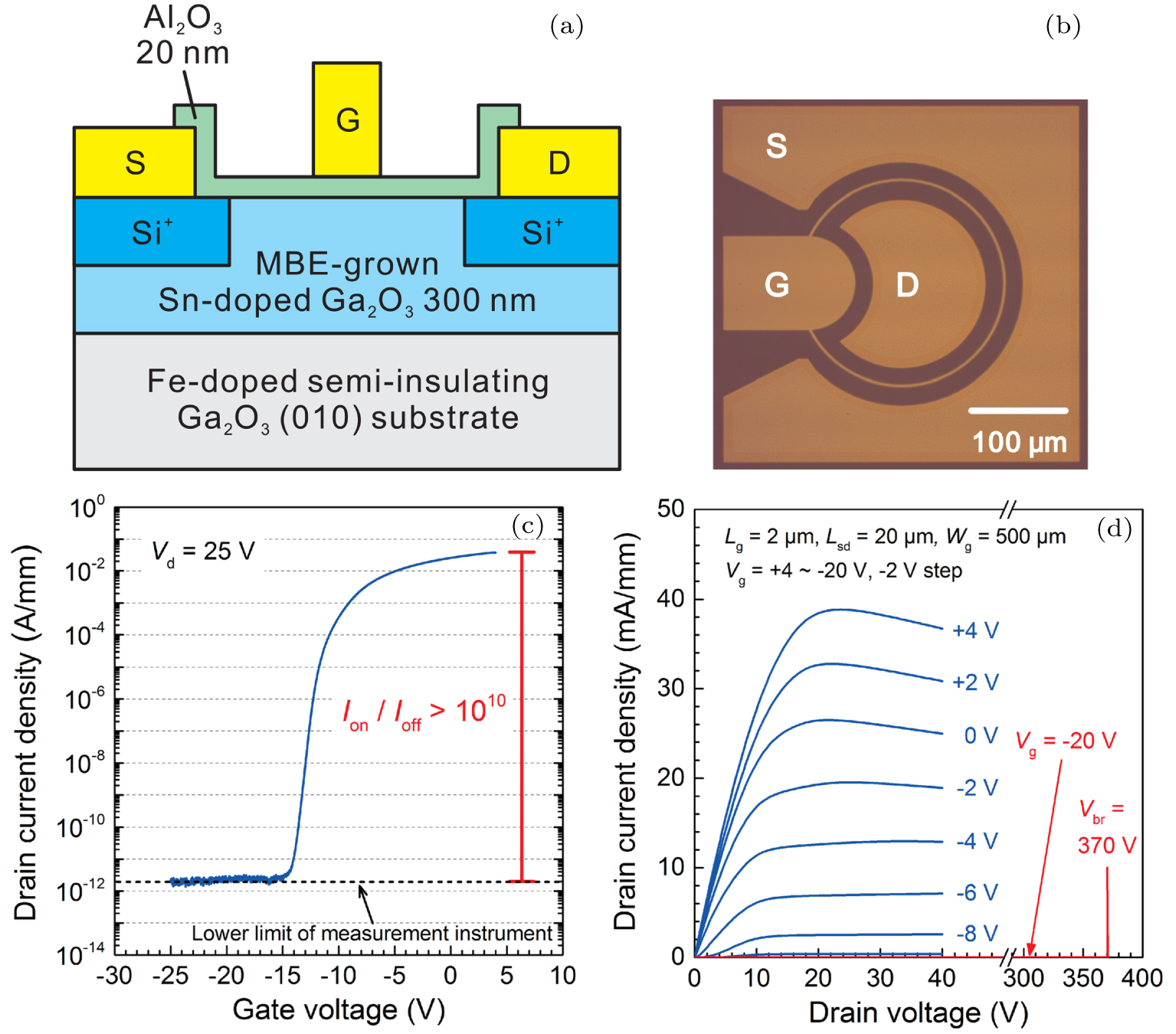
Fig. 4. Sn-doped gallium oxide MOSFET: (a) cross-sectional schematic, (b) optical microscope micrograph, (c) DC output characteristics, and (d) transfer characteristics. Reproduced with permission from Ref. [54]. Copyright 2013, AIP Publishing.
Download figure:
Standard imageWong et al. introduced a buffer layer (0.9 μm UID Ga2O3) between the Fe-doped β-Ga2O3 substrate and the Si-doped β-Ga2O3 channel layer, which not only protected the substrate from being damaged by ions, but also kept the electrical integrity of the channel layer. An enhanced diffusion caused by the interaction between Fe and defects existed although Fe had intrinsic thermal stability. Owing to the existence of the UID buffer layer, the threshold voltage (Vth) increased from −17 V to −27 V.[56]
For Ga2O3 based field-plated (FP) MOSFET with SiO2 supporting the FP and passivating the device surface, IDS, a temperature-sensitive electrical parameter, can be modulated by high temperature, and the device can achieve faster output response.[57] Si-implanted n-channel FP-MOSFET successfully achieved a high Vbr of 755 V.[58] The breakdown field Ebr was 0.5 MV/cm under the condition of LGD = 15 μm, however, such a high breakdown voltage was attributed to its relatively large channel length, Ebr still did not approach the critical value of 8 MV/cm. The maximum drain current density was ∼ 78 mA/mm when VGS was 4 V. Pulsed IDS matched or exceeded the DC values (pulse-width 100 μs and 0.1% duty cycle), and the Ion/Ioff declined from 109 to 103 as the operation temperature increased from 25 °C to 300 °C.[58]
The fabricated Ga2O3 devices can work well in the harsh environment, e.g., space full of high-energy particle irradiation, no obvious difference was found from the normal operational devices.[59,60] Low energy consumption enhancement-mode (E-mode) β-Ga2O3 based MOSFET, with 50 nm Al2O3 thin film as gate dielectric layer, was illustrated in Ref. [61], the gate metal stack with a length of 14 μm fully covered the channel region to deplete the 4-μm actual channel. However, the unsatisfied current of 1.4 mA/mm showed that the long gate did not deplete the all-cover region though the Ion/Ioff was 106. The detailed electric field distribution under the gate modulation was not further investigated (inside or beyond the 4 μm actual channel region), so it is hard to point out where the effective gate segments were in this device.
It is worth noting that in Ref. [62], the gate metal stacks were separated by an Al2O3 dielectric with a channel layer only in the contacted parts with drain and source, the breakdown voltage was improved to 230 V via dielectric optimization. The calculated Ebr (Vbr/LGD = 230 V/0.6 μm) was ∼ 3.833 MV/cm, which surpassed the theoretical limitations of SiC (3.18 MV/cm) and GaN (3 MV/cm). The maximum drain current was ∼ 60 mA/mm, board peak gm across 15 V showed that the gate could better modulate the drain current on large VGS extents, and the drain current on/off ratio was about 107. The two-finger MOSFET revealed an enormous potential in Ga2O3 based power device applications to endure larger and larger breakdown fields within its scope of the material's theoretical limit.
A high breakdown voltage of over 600 V was realized in a wrap-gate fin-FET on native (100) substrate.[63] The breakdown field was calculated according to its Vbr and device size, i.e., Ebr = 0.35 MV/cm (LGD = 16 μm) or 0.29 MV/cm (LGD = 21 μm). The maximum drain current was ∼ 3.5 μA (LSD = 4 μm), and the drain current density was about ∼ 0.875 mA/mm. The subthreshold slope (SS) was as low as 158 MV/dec (the gate voltage was increased by one order of magnitude for the drain current), and the drain on/off current ratio was over 105, attesting that this device had a good switching capability. At VGS = 0 V, the device was off, such a normally-off (E-mode) operation is preferred for safe during high-voltage operation and low off-state dissipation.
Recessed-gate type radio-frequency (RF) MOSFET[64] fabricated by metal–organic vapor phase epitaxy (MOVPE) was also investigated. The achieved normally-on (D-mode) Si-doped MOSFET had a drain on/off current ratio up to 106, meeting the requirement for practical application. The parameter gm was 21.2 mS/mm, indicating that IDS could be modulated by VGS effectively. Under a small extrinsic RF operation signal, the device had a cutoff frequency (fT) of 3.3 GHz and maximum oscillating frequency (fmax) of 12.9 GHz. The results verified that β-Ga2O3 had strong potential applications in the field of power electronic switching and RF-devices fabrication. Singh et al.[65] reported a field-plated β-Ga2O3 MOSFET driven by a pulsed continuous-wave (CW) large radio frequency signal. The heating problem in the channel was remitted to some degree by the pulsed measurements, and an out power density of 0.13 W/mm and a maximum gain of 4.8 dB at 1 GHz were achieved.
Recessed-gated E-mode MOSFET was studied by Chabak et al.[66] They deposited 200-nm Si-doped β-Ga2O3 thin film as the channel layer. The saturated drain current of the device reached up to 40 mA/mm at VGS = 8 V. Transconductance gm was 7 mS/mm, which showed good modulated capability of gate voltage on drain current, and the drain on/off current ratio was ∼ 109. From the data extracted from the three-terminal breakdown tests, an ideal Ebr = 1.98 MV/cm (LGD = 1 μm, Vbr = 198 V) or Ebr = 1.44 MV/cm (LGD = 3.5 μm, Vbr = 505 V) was obtained. In contrast with others, this transistor implemented a relatively high value of breakdown field for Ga2O3 devices. A recessed type gate of this kind occupied partial channel layer and fully depleted the channel under the 1-μm gate region even at VGS = 0 V (normally-off E-mode). Lv et al.[67] studied the effects of recessed gate on FET performances in a Si-doped β-Ga2O3 MOSFET with 25 nm HfO2 as the gate dielectric. The saturation drain current declined from 20.7 mA/mm to 2.6 mA/mm when the recess depths increased from 110 nm to 220 nm, while the threshold voltage shifted from −4.9 V to 3 V. Such preferable performances were mainly due to the contributions of the recessed gate by suppressing the electric field close to the gate side.
Moser et al.[68] used a pulsed measurement method to reduce the self-heating effects caused by the low thermal conductivity of Ga2O3.[69,70] They used this method to measure an Sn-doped β-Ga2O3 thin film based MOSFET with 20 nm HfO2 as the gate dielectric layer. The obtained maximum drain current was 478 mA/mm at VGS = 4 V, and the drain on/off current ratio was ∼108. The reported results demonstrated that the pulsed method can remit the self-heating effects to some extent, thus the device can be operated at higher voltage than the device operated by DC measurement method.
Compared with Si- and Sn-doped β-Ga2O3 channel layers,[71] the Ge-doped β-Ga2O3 channel layer grown by MBE had a high carrier concentration of 4 × 1017 cm−3 and carrier mobility of 111 cm2/(V·s) at room temperature (RT).[72] This device gave out a saturated drain current density of 75 mA/mm at VGS = 0 V. Smaller hysteresis meant as fewer number of traps at the Ga2O3/Al2O3 interface that contributed to high Ion/Ioff of 108. Breakdown occurred between gate and drain at Vbr of 479 V. Given the LGD of 5.5 μm, the calculated Ebr was about 0.87 MV/cm. The transistor was on at the bias of 0 V, and was named the normally-on D-mode MOSFET.
Krishnamoorthy et al. developed a method, named the delta/pulsed method, to fabricate β-Ga2O3 based transistors by depositing UID β-Ga2O3 and Si-doped β-Ga2O3 films alternately on Fe-doped (010) β-Ga2O3 substrate.[73] The fabricated MOSFET had a saturated drain current up to 236 mA/mm at VDS = 7 V and VGS = 2 V. Three-terminal breakdown occurred at VDS = 35 V (Vbr = 35 V, LGD = 17.5 μm), so the calculated Ebr was 0.02 MV/cm. The Si-doped β-Ga2O3 thin films grown by this method could achieve high electron mobility and high charge density.[42,43,73]
First β-Ga2O3 based MOSFET fabricated by MOVPE on heterogenous substrate (c-sapphire) was demonstrated by Tadjer et al.[74] This normally-off E-mode device was turned on at threshold voltage Vth = 4.7 V, the saturated drain current was 42 nA, and no breakdown measurement was taken. The leakage current in the device could not be neglected because of the low conduction-band offset between the gate dielectric layer and channel layer.[75,76] To improve the device performance, an in-depth understanding of dopant incorporation and defect evolution during the channel layer growth is needed.
A dual-gate transistor based on β-Ga2O3 exfoliated membrane was designed and fabricated by Ahn et al.[77] The exfoliated 200-nm β-Ga2O3 membrane was transferred onto a Si/SiO2 substrate as the channel layer, 15-nm Al2O3 and 300-nm SiO2 were employed as the top-gate and back-gate dielectrics layers, respectively. The device could operate stably under top-, back-, or both gate modulations, and the saturated drain current up to 60 mA/mm and on/off ratio of quintillion were obtained. Kim et al. fabricated an exfoliated β-Ga2O3 membrane based dual-gate MOSFET on p-type Si substrate using h-BN as the top-gate dielectric layer and SiO2 as the back-gate dielectric layer.[78] The turn-on voltage, Ion/Ioff, and SS were −48/−24 V, 106/107, and 502/348 MV/dec for back- and top-gate modulations, respectively. Figure 5 shows the schematic diagram of the dual-gate MOSFET structure. Work similar to Ref. [78] was done by Kim with WSe2 instead of h-BN as the gate dielectric.[79] These layered materials combined with gallium oxide provided a way to fabricated low-dimension power devices.
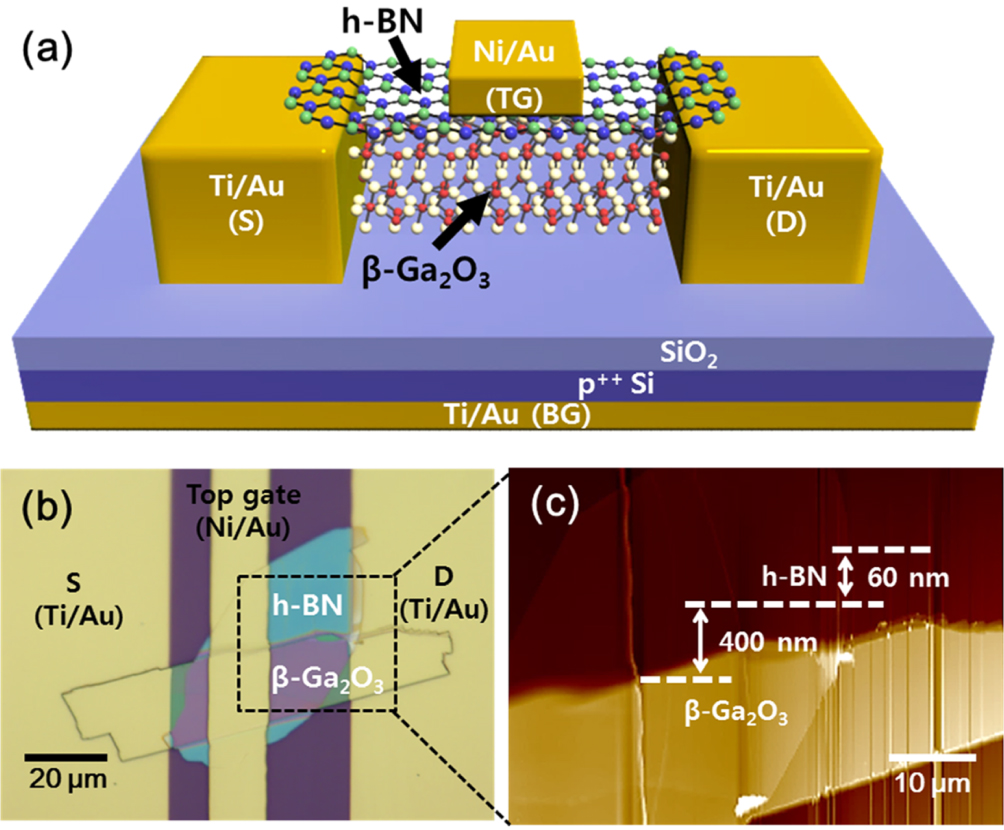
Fig. 5. (a) Schematic of a β-Ga2O3 FET with h-BN as dielectric on Si/SiO2 substrate, (b) optical image, (c) AFM image of the device. Reproduced with permission from Ref. [78]. Copyright 2017, American Chemical Society.
Download figure:
Standard imageTadjer et al. fabricated the first exfoliated β-Ga2O3 membrane based normally-off E-mode MOSFET with a threshold voltage of 2.9 V.[80] The transistor was different from the back-gate transistors mentioned above in this section, it was made on (001) β-Ga2O3 single crystal substrate with 42 nm HfO2 as the top-gate dielectric layer to reduce the leakage current. Three-terminal breakdown occurred at VDS = 80 V, and the calculated Ebr was ∼ 0.16 MV/cm (LGD = 5 μm).
Zeng et al. fabricated a lateral MOSFET by using 200-nm UID Ga2O3 as the buffer layer, Sn-doped β-Ga2O3 as the channel layer, and 2-nm SiO2 as the gate dielectric layer.[81] The obtained Vbr was as high as 382 V with LGD of 10 μm, then the calculated Ebr was 0.38 MV/cm, the switching capacity Ion/Ioff was ∼108, and the maximum drain current density was 35 mA/mm.
Recently, Zeng et al.[82] fabricated a FP-MOSFET with the highest Vbr of 1850 V and Ebr of 4.4 MV/cm until now. In this device, UID Ga2O3 buffer layer and MBE-grown Sn-doped β-Ga2O3 channel layer were successively deposited on Fe-doped β-Ga2O3 substrate, 420-nm ALD/PECVD/ALD-grown oxide layers were deposited on the channel layer, while thin Al2O3 etch stop layer was deposited by ALD between the 20 nm SiO2 gate dielectric layer and 350 nm PECVD-grown SiO2 layer. The breakdown field of 4.4 MV/cm exceeded half of the theoretical value of 8 MV/cm, this reported result produced a big step forward in developing the Ga2O3 based power devices.
Sasaki et al.[83] achieved a D-mode vertical MOSFET by utilizing HVPE-grown homoepitaxial Ga2O3 films as the channel layer and HfO2 as the gate dielectric layer. The devices presented a low on-state resistitvity of 3.7 mΩ·cm2, while the Ion/off was only 103 due to serious gate leakage. Wong et al.[84] put an Mg-doped blocking layer between the drain and source for electric isolation and only opened an aperture for drain current transform in vertical β-Ga2O3 MOSFET. Unfortunately, the Mg diffusion degenerated the off-state characteristics and peak transconductance to some extent, and the results obtained from experiments were inferior to the simulations.
Lately, Hu et al.[85] developed an E-mode vertical β-Ga2O3 MOSFET with preferable device performances, the HVPE-grown fin-shaped channel layer was deposited on a Ga2O3 (001) single crystal substrate. Without field plate, the device achieved a high breakdown voltage of 1057 V due to the low charge concentration of ∼106 cm−3 and turned on at VGS of 1.2–2.2 V (normally-off, E-mode). Its Ion/Ioff and Ron were 108 and 13–18 Ω·cm2, respectively. They also found that a wider channel could lead to a low drain-induced barrier, so that the transistor would break down ahead of schedule.[86] Traps in gate dielectrics might limit the field effect mobility in the channel of transistors, and eventually affected the drain current and breakdown voltage.
The study of the β-(AlxGa1−x)2O3 alloy, unlike β-Ga2O3, is still at a very early stage. The bandgap of up to 6 eV and the maintenance of a β phase under the condition of x < 0.7 provides an opportunity for the β-(AlxGa1−x)2O3 alloy to be employed in high voltage electronics.[87–90] Ahmadi et al.[89] developed a β-(AlxGa1−x)2O3/Ga2O3 hetero-structured MOSFET with Ge as dopant to generate 2DEG in Ga2O3. This device achieved a maximum drain current density of 20 mA/mm and pinch-off voltage of −6 V with a 2DEG charge density of 1.2 × 1013 cm−2.
Russell et al.[91] simulated the device by replacing the homogeneous substrate with 4H-SiC single crystal whose thermal conductivity is almost 30 times that of Ga2O3. Such a change could reduce the inner heating effect in the device, thus largely improving the drain current for better device performance.[92]
2.3. Back-gated FET
Hwang et al.[93] fabricated an exfoliated β-Ga2O3 membrane based MOSFET by using a heavily doped Si substrate as the back-gate, and SiO2 as the dielectric layer. The drain and source Ohmic contacts were patterned by conventional lithography technique on the channel layer. The structure of the device is shown in Fig. 6(a). The mobility was ∼ 70 cm2/(V·s), Ion/Ioff was ∼107 at VDS = 20 V, and the SS was 200 MV/dec. The high SS value means that the device can be modulated by the gate very well. The exfoliated β-Ga2O3 membrane based MOSFETs also highlighted their high-voltage operation capability (Fig. 6(c)), and had better performance than the MoS2 based transistors. In addition, it should be mentioned that the exfoliated β-Ga2O3 membrane based transistors had better performance than the transistors employing β-Ga2O3 thin films deposited by MBE and MOPVE methods for most reported research, which might be due to the existence of defects produced in the process of film deposition.[94] The thickness and doping concentration of the exfoliated Ga2O3 membrane were actually out of control in the process of device fabrication, which may restrict its industrialization and mass production. Compared with exfoliated Ga2O3 membrane, the properties of homo-epitaxial thin film can be easily controlled after optimizing the epitaxial deposition parameters.

Fig. 6. (a) Cross-sectional TEM image of β-Ga2O3 FETs, showing the flat interface between β-Ga2O3 and SiO2 dielectrics as well as between β-Ga2O3 and Ti/Au electrode. (b) Transfer characteristics of β-Ga2O3 FETs with channel width/length = 1/3 μm. (c) Common-source output characteristics of β-Ga2O3 and MoS2 FETs. Reproduced with permission from Ref. [93]. Copyright 2014, AIP Publishing.
Download figure:
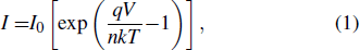
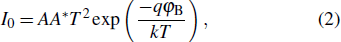
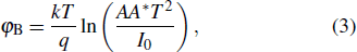
Standard imageZhou et al. transferred dozens of nanometers exfoliated membranes on Si/SiO2 (300 nm) substrate to construct FET, and they obtained a drain current of 1.5/1.0 A/mm under D-/E-mode, which are the highest values reported up to now. The experimental results are shown in Fig. 7.[95] The saturated drain current was ten orders of magnitude of the pinch-off current, and the breakdown field was as high as 2 MV/cm. Such a good performance by the device was possibly attributed to the high quality of the exfoliated membrane. To solve the problem of low thermal conductivity of Ga2O3, they used a sapphire substrate instead of a Si substrate, which significantly improved the drain current.[96] SiC is not suitable to be used as the substrate for solving the problem of self-heating effects in Ga2O3 based transistors due to its lower bandgap and higher cost, even though it has much larger thermal conductivity than sapphire.[91]
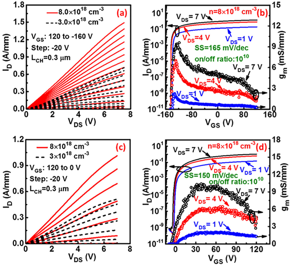
Fig. 7. (a), (c) The IDS–VDS output characteristics of D-mode and E-mode GOOI FETs with 3 × 10¹⁸ and 8 × 1018 cm−3 doping channels, respectively, ((b), (d)) IDS–gm–VGS transfer characteristics of D-mode and E-mode GOOI FETs with 8 × 1018 cm−3 doping channels, respectively. Record high IDS,max of 1.5 A/mm and 1.0 A/mm are demonstrated for D/E mode devices. Both D- and E-mode devices have high on/off ratio of 1010 and low SS of 150–165 MV/dec for 300 nm SiO2. Reproduced with permission from Ref. [95]. Copyright 2017, AIP Publishing.
Download figure:
Standard imageThe thickness of the exfoliated membranes is one of the key parameters for fabricating transistors. Zhou et al. fabricated transistors by using the exfoliated Ga2O3 membranes with different thicknesses, and studied their properties. They found that the Vth of the fabricated device was greatly dependent on the thickness of the exfoliated membrane, and the turned-on voltage even shifted from a positive to a negative value with the increase of the thickness.[97] Son et al.[98] employed exfoliated nanoscale flakes to fabricate FETs, in which the thickness of the channel layer can be modified by the photo-enhanced H3PO4 wet etching, the results showed that the threshold voltage can be controllably tuned by the thickness of the Ga2O3 flakes.
Ma et al.[99] reported the electrical properties and thermal instability of β-Ga2O3 nanoflakes based FET with SiO2 as the back-gate dielectric. The fabricated device exhibited a high field-effect mobility of 60.9 cm2/V·s, an Ion/Ioff of 109, and an SS of 210 MV/dec. However, the threshold voltage shifted under the negative bias-temperature stress at 80 °C as well as under temperature-dependent transfer characteristics up to 200 °C.
2.4. Brief summary on FET
Up to now, the Ga2O3 based FETs have been studied in top- and back-gated structures with MBE, MOVPE, HVPE, and exfoliated films. In these devices, Al2O3, SiO2, HfO2, WSe2, and h-BN were used as the gate dielectrics in the transistors. For better device performance, several problems need to be solved during the device processing and fabrication.
(I) Doping concentration In power devices fabrications, high breakdown voltage and low on-state resistance are necessary to improve the device performance. Thinner and smaller devices operating (preferred in ICs[100,101]) at the same voltages may be possible with Ga2O3 compared to the devices made with other materials. Low doping concentration of the draft layer could contribute to the high breakdown voltage (i.e., Vbr = 60(Eg/1.1)3/2·(Nd/1016)−3/4),[102] for example, doping concentration of 5 × 1015 cm−3 led to a Vbr higher than 10 kV.[103] Therefore, the study of its inherent mechanism is still in the preliminary stage, more efforts dedicated to the effects of the growth parameters on the performance of devices should be made.[104]
(II) Choices of gate dielectrics for surface passivation The gate dielectrics selected for thin film transistors should meet some requirements, such as thermal stability with the channel materials and chemical stability during the processing, high-quality interface with the channel layer, the conduction and valence band offset that are over 1 eV to act as a barrier for electrons and holes transform, as well as reliability.[5,105] What is more, high-k dielectrics should be used in MOSFET for reducing the leakage and improving the switching capability.[106] The conduction band offsets of Al2O3,[76,107] SiO2,[108,109] ZrO2,[110] HfO2,[110] LaAl2O3,[111] and AlN[75] are 1.5–2.2 eV, 3.1–3.6 eV, 1.2 eV, 1.3 eV, 2.01 eV, and 1.39 eV with β-Ga2O3, respectively. Due to the large bandgap of Ga2O3, the gate dielectrics the preferred materials are the materials with larger bandgap. Overviewing the Ga2O3 FET, Al2O3 and SiO2 are used frequently at present.
(III) Interface trap density Traps at the dielectrics and channel interface due to the existence of defects[45] and band offsets of semiconductor–dielectric[112] may seriously affect the field effect mobility, channel transport, threshold voltage stability, and device reliability. The interface trap density plays a key role in governing the active carrier concentration at the dielectrics and channel interface that will degenerate the device performance (such as carrier transport across the channel layer and gate leakage).[43,45] According to some reported works, interface quality improvements had been achieved by piranha pretreatment and post-annealing to reduce the interface trap's density.[44,113,114] In future work, further optimizing the interfaces with less traps will be a path to obtaining better device performances.
(IV) Ohmic contacts for drain and source Ohmic contact is very important for MOSFET in the source and drain regions, but it is hard to realize for UID or low-doped epilayers.[115] For this, many methods, e.g., pre-treatment,[11,55,114] post-treatment,[116] multilayer metal electrode,[117] and padding interlayer,[118,119] were developed to make Ohmic contact between metal and semiconductor. However, the surface states may cause unforeseen damage during pre-treatment (such as RIE),[120] so the multilayer metal electrode and interlayer were more favorable to be employed to form Ohmic contact during the device's fabrication processes. Ti/Au,[11,54,58,59,80,81,94,116] Ti/Al/Au,[95,97] and Ti/Al/Ni/Au[31,63] metal electrodes have been deposited on Ga2O3 to form Ohmic contact. The work function of Ti and electron affinity of UID β-Ga2O3 are known to be 4.33 eV and 4.00 ± 0.05 eV, respectively,[121] and the low barrier between Ti and Ga2O3 indicated that Ti was a good candidate for forming Ohmic contact with low resistance in contrast to other metals. However, the studies of different electrical contacts of Ti/Au, Ti/Al/Au, and Ti/Al/Ni/Au to Ga2O3 are still scant. Therefore, more research on good Ohmic contacts between metals and Ga2O3 should be put on the agenda.[122]
(V) Thermal issues The low thermal conductivity of Ga2O3 is a non-negligible problem that heavily influences carrier mobility and degenerates device performances. For solving such a problem, there are two possible ways, one is using the substrate with larger thermal conductivity to improve the thermal diffusion of the device, and the other is using the pulsed current measurement method instead of direct current measurement during the device operation to reduce the production of heat and increase the thermal diffusion time.[92,101]
3. Schottky barrier diode
Schottky barrier diodes (SBDs) are the main components of switches or rectifiers. The device performance is described by the parameters of ideality factor (n), Schottky barrier height (φB), forward current (Iforward) at specific bias, on-state resistant (Ron), and reversed breakdown voltage (Vbr). Research on metal–semiconductor (M–S) contacts are very necessary because Schottky contacts with controllable Schottky barrier heights (SBHs) and Ohmic contacts with low series resistance are the basic requirements for achieving better device performances.[123–125] Here, we present a summary about Ga2O3 based SBDs according to their different structures and metal choices of M–S contacts. Device operational characteristics can be described by the thermionic emission theory (TE theory), which was built by Bethe in 1942.[125] The TE theory shows that carriers with abundant thermal energy facilitate current transport to overcome the barrier at the M–S interface
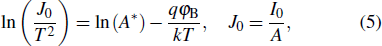
where I0 is the reverse saturation current, A is the area of the M–S contact, A* is the effective Richardson constant, V is the bias applied to the SBDs anode, n is the ideality factor, k is the Boltzmann constant, and φB is the SBH. From Eq. (2), SBHs can be calculated from
where h is the Plank constant, q is the elementary charge, A* is calculated to be 41.1 A/cm2·K2 by taking the electron effective mass of β-Ga2O3 to be m* = 0.342m0,[126,127] and m0 is the free electron mass. Figure 8 shows the basic SBDs structure (a) without and (b) with epitaxial films.
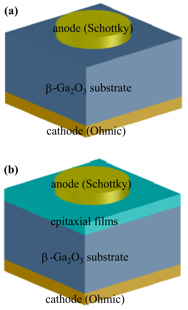
Fig. 8. Schematic diagram of SBDs based on single-crystal substrate (a) without and (b) with epitaxial films. Ti/Au ohmic electrodes are always used as the cathode and fully patterned on the back surface of substrates, anode is usually circular type (a) on the top surface of the substrate or (b) on the epitaxial film.
Download figure:
Standard imageIn the following sections, we will sum up the electronic behavior of Ga2O3 based SBDs with various Schottky metals, i.e., Pt/Ga2O3, Ni/Ga2O3, Au/Ga2O3, Cu/Ga2O3 SBDs.
3.1. Pt/Ga2O3 SBDs
For the highest metal work-function,[128,129] Pt has been widely employed in Schottky devices.[130–132] In 2013, Sasaki et al.[127] deposited a Pt circular electrode with a diameter of 100 μm on (010) β-Ga2O3 single crystal substrate with a thickness of 600 μm to fabricate SBD. The SBH between Pt and β-Ga2O3 was 1.3–1.5 eV, which was larger than those of Pt/6 H-SiC (1.06–1.33 eV),[133] Pt/4H-SiC (1.39 eV),[134] and Pt/GaN (1.11–1.27 eV),[135] the catastrophic breakdown occurred at the cathode edge and Vbr was 150 V, and the ideality factor was 1.04–1.06 close to unity. With 1.4 μm epitaxial β-Ga2O3 films (carrier concentration ranged from 1016 cm−3 to 1019 cm−3 by Sn dopant), the devices exhibited a breakdown voltage of 100 V and the Ron was 2 mΩ·cm2.[136]
The Pt/β-Ga2O3 based SBD was fabricated with 7-μm Si-doped β-Ga2O3 epitaxial layer deposited by HVPE on an Sn-doped (001) β-Ga2O3 substrate,[137] and the device characteristics followed the TE theory (Eq. (1)). Temperature had little effect on the ideality factor, the SBHs decreased only from 1.15 to 1.09 with the temperature increasing from 21 °C to 200 °C. Using Eq. (2), Richardson's plot can describe the relationship between ln(J0/T2) and 1/(kT), and this plot may verify the accurate descriptions of SBD's electric behavior by the TE theory
where J0 is the reverse saturated current density. By fitting the curves in Fig. 9(c), the SBH of 1.15 eV and A* of 55 A/cm2·K2 were determined from the slope and ordinate intercept, respectively, the value of A* did not deviate too much from the corresponding theoretical value of 41.1 A/cm2·K2, showing that the TE theory was valid in governing the SBD behaviors. The n value of 1.03 ± 0.01 was taken from Fig. 9(b) based on the TE theory.

Fig. 9. (a) Temperature dependent qVbi,0 and qφb,0 for Ga2O3 SBDs. (b) Forward J–V–T characteristics and (c) Richardson's plot [ln(J0/T2)vs. 1/(kT)] of Ga2O3 SBD in the temperature range of 21–200 °C. Reproduced with permission from Ref. [137]. Copyright 2016, AIP Publishing.
Download figure:
Standard imageBesides Pt, Tadjer et al.[138] also used 65 nm TiN as anode, and the forward and reverse I–V curves are shown in Fig. 10, from which we can obtain that the  based SBD turned on at non-zero bias at 30 °C, and such a turn-on voltage was sensitive to the temperature. The extracted SBHs and n based on the TE model suggested that TiN was also a good candidate as electrode for forming SBD with β-Ga2O3.
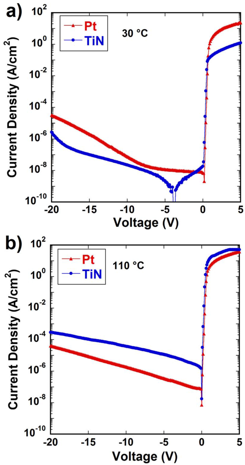
Fig. 10. Current–voltage characteristics for Pt-based and TiN-based Schottky contacts to  at (a) 30 °C and (b) 110 °C. Reproduced with permissiosn from Ref. [138]. Copyright 2017, Electrochemical Society.
Download figure:
Standard imageThe FP-MOSFET has achieved the highest breakdown voltage of 1850 V.[82] Following this, Konishi et al.[139] applied field plates to the SBD devices, i.e., FP-SBDs. The Pt/Ga2O3 SBD was fabricated by depositing HVPE-grown Si-doped β-Ga2O3 epitaxial films on Sn-doped β-Ga2O3 single crystal substrates. The 300-nm SiO2 was deposited on the epitaxial films as FP, the circular window with a diameter of 200 μm was opened for patterning the anode metals. They achieved Vbr as high as 1076 V, n of 1.03, Ron of 5.1 mΩ·cm2, and SBH of 1.46 eV, demonstrating that the device was better than most reported SBDs. Such high Vbr and low Ron demonstrated that the device was an excellent SBD.
Joishi et al.[140] fabricated a mesa Pt/β-Ga2O3 SBD on Sn-doped (010) β-Ga2O3 substrate, in which 2-μm β-Ga2O3 epitaxial film was deposited by the low-pressure chemical vapor deposition (LPCVD). The measured results showed that the on-state resistance was 39 mΩ·cm2 and the electric breakdown field in the device center was about 5.9 MV/cm as the breakdown voltage was 190 V. The Vbr changed from −138 V to −74 V due to the device surface damage caused by Ar/BCl3 plasma during the etching processes.
He et al.[141,142] and Jian et al.[143] employed (100) β-Ga2O3 the single-crystal grown by EFG method as substrate to fabricate Pt/β-Ga2O3 SBDs. The device achieved a high rectification of 1010, n of 1.1, and SBH of 1.39 eV. The forward and reverse saturated current densities were 56 A/cm2 and 2 × 10⁻¹⁶ A/cm2, respectively.[141] After that, they developed the structure by reducing the substrate thickness from 600 μm to 480 nm,[142] and substituting the UID Ga2O3 substrate with Sn-doped β-Ga2O3 single crystal. The developed device obtained the forward maximum current Imax of 421 A/cm2 and Ron of 2.9 mΩ·cm2, showing outstanding characteristics of the SBD.
The Pt/(100) β-Ga2O3 based SBD was also used in an x-ray detector by Lu et al.[144] The measured photo-to-dark current ratio was over 800, the rectification ratio was sextuple of ten, which contributed to its high forward max current and the low leakage current. An ideality factor close to unity of 1.09 accounted for that the gallium oxide was a perfect candidate in unipolar power device applications.
Besides β-Ga2O3, α-Ga2O3 is also used in devices fabrication and the devices show superior performance, examples include α-phase Ga2O3 based SBD,[145,146] FET,[40] and UV solar-blind detector.[147] The α-Ga2O3 thin films have been grown by mist-CVD,[146,148,149] mist-epitaxy technique,[145,150] and pulsed laser deposition (PLD),[147] the bandgaps of these deposited films are in the range of 5.1–5.6 eV, which are larger than those of β-Ga2O3 thin films. Oda et al.[145] fabricated SBDs based on α-Ga2O3 thin films on sapphire substrates via the mist-epitaxy growth technique. The fabricated device showed low on-resistance and breakdown voltage of 0.1 mΩ·cm2 and 531 V (diameter of Schottky electrode was 30 μm and α-Ga2O3 layer thickness was 430 nm) or 0.4 mΩ·cm2 and 855 V (diameter of Schottky electrode was 60 μm and α-Ga2O3 layer thickness was 2580 nm), respectively. Such good performance was considered to be attributed to the wide bandgap and the high breakdown field of α-Ga2O3.
The CuO2/β-Ga2O3 p–n junction based diodes were tested in the capacity of Pt/β-Ga2O3 SBD and CuO2/β-Ga2O3 diode.[151] The cross-section diagram of the fabricated device and the corresponding characteristics are displayed in Fig. 11. The diode with n of 1.31 achieved Vbr as high as 1490 V, Ron as low as 8.2 mΩ·cm2, and max forward current up to 100 A/cm2, indicating low conduction band offset at the Cu2O/β-Ga2O3 hetero-interfaces.

Fig. 11. (a) Cross-sectional schematics of the p-Cu2O/n-Ga2O3 diode and Pt/Ga2O3 Schottky barrier diode, (b) forward J–V characteristics of the p–n diode and SBD, (c) reverse J–V characteristics of the p–n diode (red) and SBD (blue). Reproduced with permission from Ref. [151]. Copyright 2017, AIP Publishing.
Download figure:
Standard imageFu et al.[152] studied the electrical properties of vertical  and (010) β-Ga2O3 SBDs based on single-crystal substrates grown by EFG. The (010) SBD had larger turn-on voltage and SBH due to the anisotropic surface properties, and the
  SBD presented more a uniform SBH distribution and a larger leakage current due to its lower SBH (thus a smaller breakdown voltage). The homogeneous SBH was also extracted, i.e., 1.33 eV for the
  SBD and 1.53 eV for the (010) SBD. These results indicated that the β-Ga2O3 crystalline anisotropy could affect the vertical SBD performances which should be paid attention to.
3.2. Ni/Ga2O3 SBDs
For lateral-type SBDs, the anode and cathode metals were deposited at grades with certain height difference, as shown in the inset of Fig. 12. Zhang et al.[153] fabricated an Ni/β-Ga2O3/Ti/Au structured SBD by depositing a metal electrode directly on the single-crystal substrate surface and realized a high SBH of 1.55 eV at 300 K,[154] the turn-on voltage decreased with the increase of temperature as shown in Fig. 12(a). On this basis, Farzana et al.[155] added an epitaxial layer grown by plasma-assisted molecular beam epitaxy (PAMBE) into the SBD structure as shown in the inset of Fig. 12(b), and they obtained n of 2.1 at 300 K, a reverse current on the order of 10 μA/cm2, SBH of 1.55 eV with a deviation of 0.2 eV, and a built-in potential of 1.41 eV, which was the intercept across the V axis in the 1/C2–V plots.[156]
Fig. 12. (a) The J–V characteristics of Ni/β-Ga2O3 (010) SBD diode between 100 K and 400 K. Inset shows the corresponding schematic diagram. Reproduced with permission from Ref. [153]. Copyright 2016, AIP Publishing. (b) J–V characteristics of Ni/β-Ga2O3 (010) SBD measured for temperatures between 80 K and 400 K. Inset shows the schematic diagram. Reproduced with permission from Ref. [155]. Copyright 2018, AIP Publishing.
Download figure:
Standard imageThe β-Ga2O3 based solar blind photodetectors with low false alarms have attracted much interest.[157–159] Armstrong et al.[160] fabricated a solar-blind detector based on  Schottky diodes, photoconductive gain of over 50 and responsivity of 8 A/W were achieved in the investigation, the SBH was as low as 1.05 eV due to the self-trapping holes at the valence band of Ga2O3.
With heavy doped  single crystal substrate grown by EFG method, Oishi et al.[161] fabricated a 10-nm Ni//600-μm β-Ga2O3 SBD with an anode diameter of 300 μm, the obtained forward current was about 96.8 A/cm2 with a resistance of 7.4 mΩ·cm2 at the bias of 1.6 V. According to the TE theory, the SBH of 0.9 eV and n of 1.4 were calculated from the I–V curves.
In the SBD based device fabrications, high ion density ICP etching processes are of the essence before the metal electrodes are deposited on the single crystal surface, which may guarantee the favorable contacts between metal electrodes and semiconductors. Yang et al. used Cl2/Ar or BCl3/Ar plasmas to etch Ga2O3, the etching results showed that the etching power, frequency, and duration had influence on the device performances.[162] For BCl3/Ar plasmas etching, the etching rate increased with the increase of ion energy, the SBH of 0.86 eV and n of 1.20 were obtained with the high etching rate processed devices, while the SBH of 1.07 eV and n of 1.00 were obtained with lower etching rate processed devices.[163]
Yang et al.[164] fabricated Ni/β-Ga2O3 SBDs by using HVPE technique to deposit Si-doped β-Ga2O3 epitaxial films on Sn-doped single crystal substrates. The devices were measured in a temperature range of 25–100 °C, the results showed that the SBHs decreased from 1.1 eV at 25 °C to 0.94 eV at 100 °C, n increased from 1.08 to 1.28 in the same temperature range, and the temperature had a stronger effect on the ideality factor than the others. The breakdown voltage shifted from 920 V to 1016 V at 25 °C when the diameter of the Ni circular anodes shrank from 210 μm to 105 μm. The Vbr is dependent on the bandgap and doping concentrations, i.e., Vbr ∼ bandgap3/2 × doping concentration−3/4.[102] After that, the circular Schottky electrode diameter shrank to 20 μm, high Vbr increased to 1600 V at RT, which was the top-class among the reported performances of gallium oxide based SBDs.[165] Using these devices, Yang et al. tested the device operations under the condition of 1.5 MeV electron irradiation, and found that the Ga2O3 based SBDs could be radiation-resistant.[166] Very recently, they illustrated an FP-type Ni/Si-doped β-Ga2O3 SBD by using SiNx as the contact window. The SiNx contact window was patterned on the surface of epitaxial films and then opened with 1:10 buffered oxide etch (BOE) solution, Schottky electrodes were patterned with the photolithography technique by overlapping 10 μm on the SiNx contact window. The Ron of 15.8 mΩ·cm2 and Vbr of 650 V made contributions to the BFOM of 26.5 MW·cm−2 (BFOM  ).[167]
Oh et al.[168] deposited UID β-Ga2O3 epitaxial films on Sn-doped β-Ga2O3 single crystal substrate to fabricate an Ni/β-Ga2O3 based SBD. The Ron decreased from 2582000 mΩ·cm2 at 25 °C to 43 mΩ·cm2 at 225 °C, together with the Vbr of 210 V, BFOM was calculated to be 17.1 W·cm2.
Both Ahmadi et al.[169] and Feng et al.[170,171] fabricated Ni/β-(AlxGa1−x)O3 based SBDs on (010) β-Ga2O3 single crystal substrates. In Feng et al.'s study, the SBHs at Ni/β-(AlxGa1−x)O3 interfaces were influenced by the temperature obviously, the results calculated from the I–V curves showed that the SBHs and n varied from 0.81 eV and 2.29 at 300 K to 1.02 eV and 1.65 at 573 K. The ultimate goal for Ga2O3 power devices is that the fabricated device can be operated not only at RT but also at high temperature and in a harsh environment. From the results in Refs. [170] and [171], we can see that the device performances (forward I–V curves) were strongly dependent on the temperature. The mean SBH of 1.38 eV and A* of 46.52 cm−2·K−2 were obtained from the corresponding Richardson plots according to the Tung model.[172] These measured results by Feng et al. were not far from the preferable values, and verified the strong potentials of β-(AlxGa1−x)O3 in power electronics of SBD.
As mentioned in the FET section, exfoliated Ga2O3 membranes have been used as channel layer materials in transistors. Very recently, researchers from Hao's group at Xidian University began to fabricate Ni/β-Ga2O3 SBD with the exfoliated β-Ga2O3 membrane.[173–175] Li et al.[173] transferred the exfoliated β-Ga2O3 membranes onto q (100) β-Ga2O3 single crystal substrate and tested the I–V characteristics in the temperature range from 300 K to 500 K. They found that the forward and reverse results followed the TE theory and Poole–Frenkel model, respectively. It is worth noting that, Hu et al.[174,175] first transferred the exfoliated β-Ga2O3 membranes onto sapphire substrate instead of Ga2O3 single crystal substrate to make lateral SBDs. Without a field plate, ideal breakdown voltages of 640 V, 850 V, 1200 V, and 1700 V were achieved on condition that Ohmic–Schottky electrodes' spacings were 4 μm, 6 μm, 11 μm, and 15 μm, while the corresponding Ron were 47 Ω·mm, 66 Ω·mm, 91 Ω·mm, and 190 Ω·mm, respectively.[174] With a field plate, the breakdown voltage surpassing 3 kV (exceeded the high value of 2300 V in vertical structure with Ni as Schottky metal[176]) was achieved with the Ohmic–Schottky electrode spacing of 24 μm. The four-star DC power figure of merit of 370 MV/cm2, combined with the high breakdown voltage, suggesting a huge potential of Ga2O3 employed in power rectifiers.[175]
3.3. Other metals/Ga2O3 SBDs
Farzana et al.[177] fabricated SBDs by using four different metals, i.e., Ni, Pt, Pd, and Au, and then studied their properties systematically. The I–V curves, ideality factors, and SBHs are shown in Fig. 13. The transport properties of the Schottky barriers formed by Ni/Ga2O3, Pt/Ga2O3, and Pd/Ga2O3 were all governed by the TE theory, but that formed by Au/β-Ga2O3 was different, because the A* derived from the I–V curve of Au/β-Ga2O3 SBD was 3.2 × 10⁻⁶ A/cm2·K2, far less than the standard value of 41.1 A/cm2·K2. The M–S (Au/β-Ga2O3) contact was complex beyond the TE theory, and the spread of SBHs caused by the inhomogeneous interface was suggested to be the reason leading to such a phenomenon.[177,178]

Fig. 13. (a) The I–V characteristics of UID (010) β-Ga2O3 SBDs of Pd, Ni, Pt, and Au, and (b) internal photoemission measurement (IPE) results at 300 K. Reproduced with permission from Ref. [177]. Copyright 2017, AIP Publishing.
Download figure:
Standard imageYao et al.[179] deposited (010) β-Ga2O3 epitaxial films by MOCVD on  single crystal substrate to fabricate SBDs by taking W, Cu, Ni, Ir, and Pt as Schottky metals. The SBHs extracted from the C–V curves in the range of 1.6–2.0 eV were larger than those extracted from the I–V curves in the range of 1.0–1.3 eV. They also found that the SBHs were little correlated with the work function of the metal while the surface defects and unpassivated surface states affected the diodes' electric behavior dominantly.
Earlier in 2014, Splith et al.[180] used Cu as electrodes to fabricate  SBDs, in which the Ga2O3 epitaxial films were grown by PLD on c-plane Al2O3 substrates. The lateral structure (f–f geometry as described in Ref. [180]) device had the SBH of 0.92 eV and n of 1.22. The SBHs, with a mean value of 1.32 ± 0.05 eV, depended linearly on the temperature according to the TE theory.
Sasaki et al.[181] and Liu et al.[182] used Au electrodes to contact Ga2O3 epitaxial films on Si-doped β-Ga2O3 single crystal substrates to fabricate Au/(010) β-Ga2O3 and Au/(101) β-Ga2O3 SBDs, respectively. Sasaki et al. obtained a good performance of his SBD with n of 1.13 and Vbr of 125 V.[181] Liu et al.[182] achieved photoresponsivity of 1.8 A/W with MBE-grown high resistivity membrane on a Si-doped β-Ga2O3 substrate. However, this SBD could not operate well due to its n of over 30 that was much larger than unity.
The surface dielectric also plays a key role in governing the device performance. Shahin et al.[183] deposited high-k HfO2 (k ∼ 14) layer on  single crystal substrate with Au as the anode to fabricate SBD, and then C–V and I–V measurements were executed. The low hysteresis of the dual-sweep C–V curve signified an outstanding HfO2/β-Ga2O3 interface quality. The SBD was turned on at +1.05 V, suggesting that the Au/HfO2/Ga2O3 structure was useful for obtaining the positive Vth. The introduction of HfO2 dielectric layer not only reduced the leakage current but also enhanced the devices anti-breakdown capacities. These results provided confidence in developing the Ga2O3 MOS electronic devices especially by using the HfO2/Ga2O3 interface as a structure component.
Sasaki et al.[184] demonstrated the first trench MOS-SBD with Cu as Schottky metal and HfO2 as dielectric between anode and epitaxial films, and the Si-doped β-Ga2O3 epitaxial films were deposited on Sn-doped (001) β-Ga2O3 substrate. Ron was 2.3 mΩ·cm2 and Vbr reached up to 240 V, while SBH of 0.98 eV was lower than the highest values reported.
In Yang et al.'s study,[185]  SBDs based photodetectors exhibited a high rectification ratio of 107 at ± 2 V, SBH was 0.96 eV, and n was 1.47, which was much larger than unity, high-quality crystalline enabled the low dark current and sharp cutoff wavelength of 256 nm.
3.4. Brief summary on SBDs
In the SBD section, we introduced the Ga2O3 based SBDs with or without epitaxial films as shown in Fig. 9, and the devices were fabricated based on the (010)-,  , (100)-, and (001)-oriented Ga2O3 single crystal substrates. To date, Pt, Ni, Cu, Au, and Pd/Ga2O3 Schottky diodes have been investigated. High-quality single-crystals are very important for improving the device performance of the SBDs (as well as UV solar-blind detector, transistors, and sensors).[186–188] The M–S interface is a key element that should be taken into consideration, high breakdown voltage and low on state resistance are preferable in Schottky diodes.[189] We list the following two key issues that should be paid attention to.
(I) Metal–semiconductor contact interface The M–S contact[123,190–193] is a direct key issue influencing the device performance, and the superficial structure, energy, and metal work-function should be investigated for obtaining the desired M–S contact type (Ohmic or Schottky).[191] Carrier transport is governed by the band offset and SBHs at the M–S contact interfaces,[194,195] and the high-k dielectric material may reduce the overestimation of both the carrier mobility and the leakage current,[196] which affects I–V characteristics heavily. Another important factor is the craft processes: avoiding the photoresist residual during photolithography transferring courses and suitable plasma processing make better contacts between metal electrodes and semiconductor surface.[55,114,197]
(II) The choice of metals and M–S SBH For n-type wide-bandgap semiconductors, the contact resistance usually depends on the M–S SBHs.[194,195] The Schottky–Mott rule[125] is normally used to describe the energy band alignment at the M–S interfaces, which presents the relationship between SBH (φB) and the metal work function (φm), i.e., qφB = qφm – χs, where χs is the semiconductor electron affinity.
Due to the metal-induced gap states at the metal–semiconductor interfaces, strong Fermi level pinning effects can be found in the metal–semiconductor junction.[198,199] The pinning factors S can be given as S = ∂φB/∂φm, which indicates the dependence of SBHs on the metal work function.[200] So in the Ga2O3 based SBDs, the choice of metals contacted to Ga2O3 is also a key factor to determine the SBH.
For Ga2O3, the Schottky diode electrical properties with different metals have been studied by Farzana et al.[177] and Yao et al.,[179] inhomogeneous SBH at M–S interfaces was the primary cause for non-ideal thermionic transport in an SBD. The different SBH values with the choices of metals suggested that Fermi level pinning effect did not always dominate the SBHs for gallium oxide. As only a small amount of research into Ga2O3 have been performed, the dependence of SBH on metal work function is still unclear. For a better understanding the SBHs across the M–S contact interfaces, more research should be carried out in gate metals engineering for future device applications.
4. Conclusions and perspectives
In this review, we have presented recent advances in Ga2O3 based FETs and SBDs to the best of our knowledge. Owing to its excellent properties, Ga2O3 is suitable for fabricating power electronic devices superior to SiC and GaN counterparts. It is expected to dominate the power devices market in the near future. To date, Ga2O3 based power devices are still in the early stage of development, so the in-depth study of the materials properties and devices fabrication technologies is necessary and urgent.
Reviewing the developments of other semiconductor devices,[201–205] we find that the properties of Ga2O3 and relevant microelectronics are still at early stages and need to be clarified. Based on the existing achievements on Ga2O3,[206–211] intensive attention should be paid to research and development of Ga2O3 power electronic devices in order to promote the industrialization of Ga2O3 electronic devices.
Acknowledgment
Zeng Liu is grateful to Dr. Yan Zhang, Dr. Tao Wang (Fudan University, Shanghai, China), and Dr. Yong Wang (Dalian University of Technology, Dalian, China) for their useful discussion.
Footnotes
- *
Project supported by the National Natural Science Foundation of China (Grant Nos. 61774019, 51572033, and 51572241) and the Beijing Municipal Commission of Science and Technology, China (Grant No. SX2018-04).