
Abstract
Two-dimensional (2D) materials have recently received a great deal of attention due to their unique structures and fascinating properties, as well as their potential applications. 2D hexagonal boron nitride (2D h-BN), an insulator with excellent thermal stability, chemical inertness, and unique electronic and optical properties, and a band gap of 5.97 eV, is considered to be an ideal candidate for integration with other 2D materials. Nevertheless, the controllable growth of high-quality 2D h-BN is still a great challenge. A comprehensive overview of the progress that has been made in the synthesis of 2D h-BN is presented, highlighting the advantages and disadvantages of various synthesis approaches. In addition, the electronic, optical, thermal, and mechanical properties, heterostructures, and related applications of 2D h-BN are discussed.
Export citation and abstract BibTeX RIS
1. Introduction
Recently, two-dimensional (2D) materials have attracted significant attention due to their unique structures, fascinating properties, and potential application[1]. Graphene is a single-atom-thick, crystalline carbon film that exhibits various interesting properties, such as ultrahigh carrier mobility, quantum Hall effect, excellent optical transparency, high Young's modulus, and excellent thermal conductivity[2]. The surge of graphene also paved the way for the discovery of other 2D materials with similar layered structure, such as hexagonal boron nitride (h-BN), transition metal dichalcogenides (TMDCs), black phosphorus (BP), and MXenes[3]. Similar to graphene, these 2D materials with diverse chemical compositions have shown unprecedented and complementary properties, which make them promising building blocks for many future applications[4].
Boron nitride is isomorphic to carbon in various crystalline forms, including zero-dimensional nanocages, one-dimensional nanotubes, two-dimensional atomic layers and three-dimensional bulk structure[5]. Among the family of 2D materials, h-BN occupies a special position, being an insulator with a wide band gap (5.97 eV) isostructural to graphene[6–8]. It consists of alternating boron and nitrogen atoms arranged in an sp2-bonded network within each layer, and the bond length of B–N is 1.44 Å while that of C–C in graphene is 1.42 Å[9]. It was proposed that an obvious band gap would be induced in graphene aligned to a 2D h-BN substrate[10], leading to a significant increase in experimental research of h-BN. Ultimately, 2D h-BN has proven to be an ideal dielectric substrate of graphene for improved device quality due to its close lattice matching (∼ 1.6%) with graphene, as well as dangling-bond-free and atomically flat surface[4, 5]. For example, an order of magnitude improvement in carrier mobility, micrometer scale ballistic transport and quantum Hall effect have been observed in the graphene/h-BN heterostructures[11–13].
To a large extent, the structure and properties of 2D h-BN depend on synthesis methods. However, how to synthesize large-area high-quality 2D h-BN layers remains a great technical challenge for both basic and applied research. In particular, obtaining high-quality 2D h-BN requires the elimination of high-density structural defects (e.g. grain boundaries and dangling bonds) resulting from small grains[14, 15]. The defects will usually lead to higher surface roughness and charge traps, and finally the degradation of device performances[16]. Along this line, larger h-BN single domains or epitaxial growth should be achieved. Otherwise, the 2D h-BN layers with controlled thickness were needed for device applications, which can only be realized by understanding of synthesis mechanism involved in the growth process.
In this article, we review the recent progress in the synthesis of 2D h-BN. We first introduce the properties and applications of 2D h-BN. Then we discuss various approaches for the synthesis of 2D h-BN. Similar to the well-known techniques utilized for the growth of graphene, various methods have been employed to synthesize 2D h-BN, which can be classified into "top-down" and "bottom-up" approaches. In this paper, these techniques will be discussed in detail. In particular, this review will concentrate on chemical vapor deposition (CVD) as well as several novel methods, such as ion beam sputtering deposition (IBSD) and co-segregation. Finally, we point out some possible directions in the syntheses, characterizations, and applications of 2D h-BN.
2. Properties and applications of 2D h-BN
As an inheritor of bulk h-BN, 2D h-BN also exhibits a unique combination of advantageous properties, including excellent electrical insulation, high thermal conductivity, high elastic modulus, excellent inertness and low friction coefficient. These unique properties make 2D h-BN a promising candidate for a rich variety of applicationsns[5–7]. In this section, these properties and applications will be briefly discussed.
On account of the absence of free electrons as induced by the slight ionicity of the B–N bond, h-BN is electrically insulating with a direct energy gap of about 5.97 eV, thus raising its promise as a high-quality dielectric material. Generally, the carrier mobility of graphene on SiO2 is limited by scattering from charged surface states or impurities, substrate surface roughness and surface optical phonons. In contrast, the atomically smooth surface that is relatively free of dangling bonds and trapped charges, makes 2D h-BN a suitable substrate for graphene and other 2D materials[11].
What is more, the h-BN stacked with the other 2D materials mainly serves as substrate or tunneling layer. Fig. 1 summarizes the mobility of exfoliated graphene deposited on commonly used substrates, indicating the outstanding performance of h-BN as substrates[5]. As tunneling layers, the device performances were obviously enhanced in graphene or MoS2 field effect transistor (FET), as well as graphene/Si Schottky solar cells[17–19]. Very recently, 2D h-BN has emerged as a potential packaging material due to its excellent surface and electrical properties. Other 2D materials, including graphene, BP and TMDCs, supported on or encapsulated between 2D h-BN exhibit improved properties[13, 21].
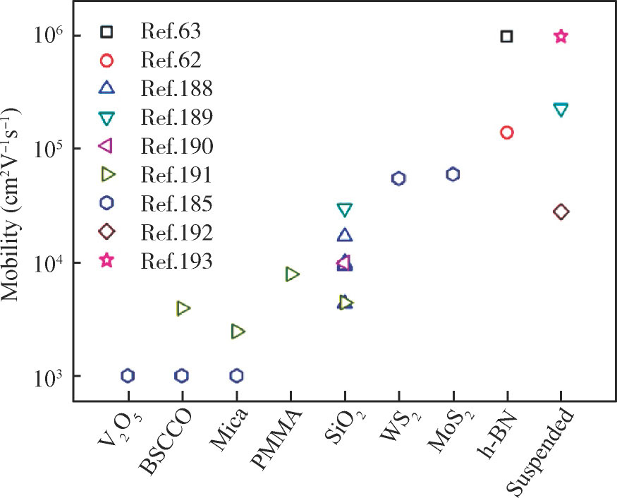
Fig. 1. Carrier mobility of exfoliated monolayer graphene supported on several typical substrates at low temperatures (1.7–20 K)[5].
Download figure:
Standard imageAmong various applications of 2D h-BN, the most attractive one is constructing van der Waals heterostructures. The controlled stacking of different 2D materials will greatly expand their family and broaden their applications. Recent years have witnessed many breakthroughs in research on combining 2D h-BN with other 2D materials, such as graphene and 2D TMDCs, to form hybrid 2D materials, as shown in Fig. 2[13, 22, 23]. The stacked structure of graphene/h-BN allows for the fabrication of graphene-based electronic devices with high performance[24, 25], while the in-plane heterostructure is very likely to be used in the construction of atomically thin integrated circuits[26, 27]. The vertically stacked heterostructures have been achieved by the layer-by-layer transfer method or the sequential growth of h-BN and graphene via a two-step deposition process[28–30]. The in-plane graphene/h-BN heterostructures were mostly synthesized by applying the so-called etching-regrowth methods[26, 27]. However, it still remains a great challenge to achieve controlled growth of the lateral and vertical heterostructures with sharp and clean interface.
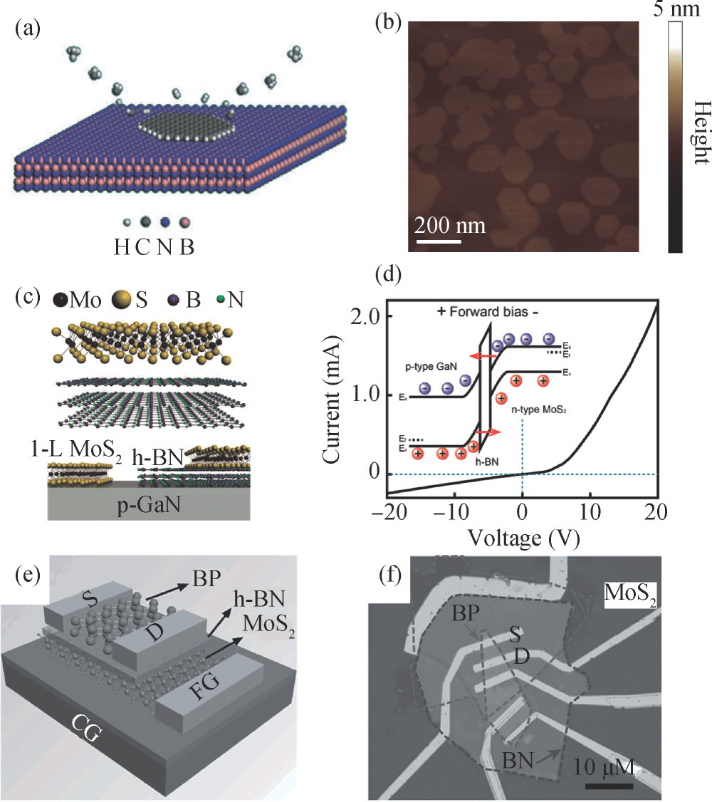
Fig. 2. (Color online) (a) Schematic illustration of the epitaxial graphene growth on h-BN. (b) Zoomed-in AFM image of as-grown graphene domains on h-BN[13]. (c) Schematic of the MoS2/h-BN/p-GaN MIS heterojunction structure. (d) I–V curves for the MIS diode[22]. (e) Schematic of the BP/h-BN/MoS2 sandwich FGFET device structure. (f) Optical micrograph of a typical fabricated device. The dotted lines indicate the boundary of each material[23].
Download figure:
Standard imageSimilar to bulk h-BN, 2D h-BN exhibits almost no optical absorption in the visible region, which enables it to show high transparency. In the deep UV range however, 2D h-BN shows a sharp absorption peak at 210–220 nm[31]. Due to its direct band gap of 5.97 eV, h-BN could be a promising candidate for fabricating DUV photodetector. Actually, the DUV photoresponse of h-BN has been demonstrated, and the prototype photodetector based on the h-BN monolayer shows a high on/off ratio when the device is illuminated by a DUV deuterium lamp[32].
Because of the absence of interlayer phonon scattering, the thermal conductivity of 2D materials, such as suspended h-BN, is expected to be higher than the basal-plane values of bulk h-BN, as shown in Fig. 3[33]. The room temperature thermal conductivity of bulk h-BN can reach ∼400 W·m−1·K−1. Theoretically, the enhanced thermal conductivity of monolayer 2D h-BN is expected to be more than 600 W·m−1·K−1[34]. The thermal conductivity of few-layer 2D h-BN was experimentally measured to be 100–270 W·m−1 ·K−1[33, 35], making it a promising heat-spreading layer in novel electronic devices or as fillers of polymeric composites[34–36]. Due to the high thermal conductivity of the h-BN nanosheets, they have been used as fillers in a mineral oil to form a stable nanofluid for application in transformers[37].

Fig. 3. (Color online) Optical micrographs showing (a) the microbridge device and (b) an 11-layer h-BN sample suspended on the device used for thermal measurement. (c) Measured thermal conductance values of four h-BN samples[33].
Download figure:
Standard imageThe Young's modulus of the few-layer 2D h-BN was measured to be 1.16 ± 0.1 TPa by nanoindentation technique, which is close to the experimental values of graphene[38]. The calculated Young's modulus of monolayer 2D h-BN is 0.71–0.97 TPa[39], but experimental verification is needed. Due to its excellent mechanical properties, 2D h-BN has been used to reinforce polymer films[40, 41].
The 2D h-BN can be stable at 1500 °C in air and will not react with most chemicals, which makes it one of the thinnest coating ever shown to withstand extreme environments, as shown in Figs. 4(a)–4(d)[42]. Besides strong resistance to oxidation, monolayer h-BN can also serve as a perfect coating to improve friction and electric resistance of the substrates, as shown in Figs. 4(e) and 4(f)[43]. This high thermal and chemical stability along with excellent coating properties make the 2D h-BN a promising coating material.

Fig. 4. (Color online) h-BN thin films as high-performance oxidation-resistance coatings. (a, b) SEM images of Cu foils after oxidization with and without h-BN coatings at 500 °C for 30 min. (c, d) SEM images of stainless steel surface with and without h-BN coatings at up to 1100 °C for 30 min. With h-BN coating, both Cu and stainless steel can maintain their original color. Without h-BN coatings, their colors have changed because of oxidation[42]. (e) Friction force signal taken on the bare Cu surface and h-BN monolayer coating on Cu at an applied load of 40 nN. (f) The deduced friction force as a function of the applied load[43].
Download figure:
Standard imageSome emerging applications of 2D h-BN were also studied in recent years. The symmetry properties of 2D h-BN monolayers endow them with piezoelectric properties, whereas the bulk parent crystal of stacked BN layers is not piezoelectric. This suggests potential for unusual electromechanical coupling properties in modern low power, high-precision technology[44, 45]. In addition, recent studies suggested that h-BN sheets can serve as a unique substrate for catalytic and sensing applications[46, 47].
3. Top-down approach
A prerequisite for the realization of diverse applications of 2D h-BN is the synthesis of high-quality h-BN layers. Typical synthesis strategies of 2D h-BN are divided into two major routes: top-down and bottom-up routes. Top-down approach for synthesis of 2D h-BN mainly includes mechanical exfoliation and chemical exfoliation. The difference between the two methods lies in the way in which the van der Waals forces between the atomic layers are broken.
3.1. Mechanical exfoliation
Mechanical exfoliation technique by Scotch was initially used to isolate graphene in 2004[48], and it has been successfully applied to the other 2D materials, such as h-BN and MoS2[49]. 2D h-BN obtained with this technique has fewer defects compared to those prepared by chemical methods, making them suitable for exploring its intrinsic properties or fundamental research in electronics and optoelectronics[50]. Nevertheless, the yield of mechanical exfoliation is extremely low, partially due to the stronger interactions between BN basal planes[51, 52]. Li et al. reported a controlled ball milling process to produce gentle shear forces that produce high quality h-BN in high yield and efficiency with little damage to the layer structure, as shown in Fig. 5[53]. The mechanical exfoliation method is the simplest route to synthesis of h-BN nanosheets, however, the limited flake size hinders their applications in large-area devices.
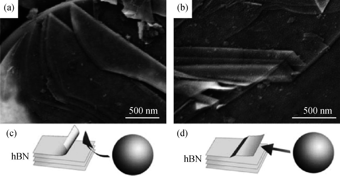
Fig. 5. SEM images and corresponding diagrams illustrating two observed exfoliating mechanisms under the shear force created by milling balls: (a), (c) cleavage from the edge of an h-BN particle; (b), (d) thin sheets peeling off the top surface of an h-BN particle[53].
Download figure:
Standard image3.2. Chemical exfoliation
Synthesis of 2D h-BN by chemical exfoliation method was first reported in 2008 by Han et al.[54]. The h-BN nanosheets could be dispersed in some organic solvents, such as chloroform and DMF, and chemical exfoliation creates dispersions of 2D h-BN with the assistance of sonication[55, 56]. Since chemical exfoliation is carried out in liquid, this method is also called liquid-phase exfoliation. Due to the stronger interlayer force of h-BN, the solvents used for the exfoliation of h-BN are usually strong solvents, such as the strong-polar DMF, Lewis bases ODA and PEG, methane sulfonic acid[57–59]. Sonication of sufficient power can break the van der Waals forces between the atomic layers of h-BN, allowing the solvent molecules to seep between the layers and expand them. Using this method, the synthesis of mono- and few-layered h-BN nanosheets was realized, as shown in Fig. 6[60]. This method is quick and easy, and insensitive to ambient conditions, leading to higher yields[61]. However, 2D h-BN obtained by chemical exfoliation suffers from surface contamination and even smaller flake size[5].
Fig. 6. (Color online) (a) Illustration of the exfoliation mechanism. (b) Typical curved nanosheets several hundred nanometers in size (circled in black). (c) A very flat nanosheet[60].
Download figure:
Standard image4. Bottom-up approach
Bottom-up routes, in which atoms are assembled in order on specific substrates through physical or chemical methods, offer significant advantages for synthesizing large area 2D h-BN compared to the top-down methods. Among bottom-up methods, CVD is the most thoroughly explored and promising for the large scale production, which is a key prerequisite for applications of 2D h-BN. Besides CVD, other novel methods have been developed for synthesizing 2D h-BN during the past several years.
4.1. CVD
The CVD technique has been applied to epitaxially grow h-BN thin films for several decades. The first h-BN monolayer was synthesized through the decomposition of B3N3H6 on transition metals such as Pt (111) and Ru (0001) in 1990[62]. It has been demonstrated that mono- and few-layer 2D h-BN have been epitaxially grown on single-crystal transition metals such as Ru (001), Rh (111), and Ni (111) with ultrahigh vacuum (UHV) systems by CVD[63–65]. Theoretical calculations and experimental results have demonstrated that 2D h-BN layers forming on 3d-transition metals and 5d-transition metals are weakly bound to the metallic substrates. However, on 4d-transition metals, the h-BN-substrate binding energy increases with the unoccupied states in the d-shell of the substrate. For instance, epitaxial h-BN monolayer can be formed on Ni (111)[65]. However, it is rather difficult to controllably grow h-BN and to transfer it onto other substrates, due to the complex nature of the UHV systems. Recently, both atmospheric pressure CVD (APCVD) and low-pressure CVD (LPCVD) have also been used to grow 2D h-BN on metallic substrates[66–69]. Considerable advances have been obtained on the fabrication of h-BN layer by CVD during the past years. In this review, we mainly focus on the synthesis of 2D h-BN using APCVD and LPCVD. As an example, the schematic diagram of LPCVD system used for h-BN growth is shown in Fig. 7(a)[69]. In the following part, we summarize the precursors, substrates and ambient gas conditions adopted in the growth of h-BN sheets, and systematically discuss the control of morphology, orientation and epitaxy, domain sizes and catalysis-free synthesis.

Fig. 7. (Color online) Schematic diagrams of (a) the low pressure CVD system used for h-BN growth[69] and (b) h-BN growth mechanism on Cu propose by Kidambi et al.[70].
Download figure:
Standard image4.1.1. Growth parameters
Similar to synthesis of graphene, realizing controllable growth to improve the crystalline quality of 2D h-BN has proved challenging, which requires a more detailed understanding of the growth process. The CVD process primarily includes the adsorption of precursor molecules on the substrate surface, the decomposition of the precursor and formation of mobile surface species, the diffusion of these species, and nucleation and/or incorporation into the growing film[61]. The growth of h-BN depends on various factors. Kidambi carried out in situ observations during CVD growth of 2D h-BN on Cu. Fig. 7(b) gives the proposed growth mechanism, which shows the most important surface processes involved in h-BN formation[70].
Precursors: CVD processes include the utilization of various gaseous, liquid or solid precursors. The gaseous precursors, such as BF3/NH3, BCl3/NH3, and B2H6/NH3, have been used to deposit 2D h-BN[71–73]. Chatterjee et al. found that thermal CVD of decaborane/ammonia mixtures on polycrystalline metal substrates can generate h-BN atomic layers[74]. For gaseous precursors, the ratio between the boron source and ammonia is the critical factor for preparing stoichiometric h-BN. However, their use has been gradually reduced for their toxicity.
Liquid precursors such as borazine (B3N3H6)[75], trichloroborazine (B3N3H3Cl3)[76, 77], or hexachloroborazine (B3N3Cl6)[78]have many advantages because of the 1 : 1 B/N stoichiometry. In particular, the decomposition of borazine does not produce the high toxic byproducts such as BF3 or BCl3. But borazine is sensitive to moisture and hydrolyzes to boric acid, ammonia, and hydrogen in water[79]. It was proposed that borazine was completely dehydrogenated at 1000 K and the morphology of h-BN depends on the substrates due to the difference in interfacial bonding[62]. Kim et al. investigated the growth mechanism of h-BN on Cu foil with borazine systematically[80]. Generally, with higher growth temperature and borazine concentration, a higher growth rate is obtained. Therefore, to obtain high quality 2D h-BN material, a lower borazine concentration should be considered.
Ammonia borane, or borazane, is a powdered precursor, which not only has 1 : 1 B/N stoichiometry but is easily accessible and more stable under ambient conditions. Borazane is a crystalline solid at room temperature and melts at around 106 °C. The decomposition of borazane produces hydrogen, monomeric aminoborane (BH2NH2) and borazine. BH2NH2 is very active and it forms polymeric aminoborane, which is a white noncrystalline solid and stable at room temperature. Therefore, the synthesis of h-BN using a borazane source is relatively complicated; the precursor should be a mixture of borazane, aminoborane, and borazine[61]. Han et al. synthesized monolayer 2D h-BN free of nanoparticles by utilizing a simple filtering system in the CVD process[81]. They attributed this to the effective removal of BN nanoparticles by the filter through restricting them from reaching the Cu substrate. In order to use it as a precursor for the CVD growth, the ammonia borane needs to be heated up to generate borazane vapor and to diffuse onto the substrates. The quality of h-BN can be tuned by simply changing the heating temperature and amount of borazane, which determine the concentration of precursor introduced into the reaction system[82].
Ambient gas condition: Typically, APCVD method was only able to obtain few layer h-BN without a good control on the number of layers. In contrast, under LPCVD growth, monolayer h-BN can be synthesized. It was reported that using LPCVD, large area monolayer h-BN was obtained on metallic substrates, such as Cu[68], Pt[83] and Co[84]. Koepke et al. systematically studied the effects of pressure on the growth of h-BN[85]. It was found that the lower pressure usually leads to h-BN which is uniform in thickness, highly crystalline, and consists solely of h-BN. At larger pressure, the growth rate increases, but the resulting h-BN is more amorphous, disordered, and sp3-bonded. This phenomenon was attributed to the incomplete thermolysis of the H3N-BH3 precursor from a passivated Cu catalyst under high pressure. Wu et al. reported that by increasing hydrogen gas flow during the growth of h-BN, the density of nucleation seeds can be decreased, leading to the formation of large-size single crystalline h-BN domain[86]. On the other hand, because monolayer 2D h-BN is not thick enough to inhibit the electron transport, controllable growth of multilayer h-BN is also important for using h-BN as a dielectric layer. APCVD holds the benefit of utilizing fewer resources, low cost and fast growth, all of which are essential for full film coverage and the mass production of 2D h-BN. For instance, Shi et al. demonstrated the synthesis of multilayer 2D h-BN on Ni foils using borazine as the precursor, while Song et al. reported the growth of multilayer h-BN on Cu foils using the ammonia borane precursor[66, 67].
Substrates: Akin to the growth of graphene, both Cu and Ni foils were the most used substrates for the CVD growth of 2D h-BN layers. Besides Cu and Ni, other metallic substrates have also been utilized for the growth of h-BN. Gao et al. reported the controlled growth of h-BN on polycrystalline Pt foils, which can be recycled repeatedly[87]. Kim et al. reported large-area multi-layer h-BN grown on Fe foil by APCVD and the thickness of the h-BN (5–15 nm) was controlled by the cooling rate[88]. Orofeo et al. reported the growth of the two, oppositely oriented, triangular h-BN domains commensurate with the Co lattice on heteroepitaxial Co metal[84]. Fu et al. reported the growth of h-BN on Ni–Ga substrates, which possess excellent sulfide-resistant properties and a high catalytic activity for h-BN growth, and they obtained TMDCs/h-BN vertical heterostructures without any intermediate transfer steps[89]. Furthermore, it was also reported that the growth of 2D h-BN exhibits obvious grain dependency. For instance, the growth rate of h-BN is larger on Ni (100)- or Ni (100)-like crystal surfaces but the growth on Ni (111)- or Ni (111)-like surfaces is non-detectable[90]. Similarly, the orientation of the h-BN domains was also confined largely by the Pt grains. At high pressure, the thicker film was grown on Pt (111), and in contrast, the thinner film was grown on Pt (001)[83]. Kim et al. investigated the influence of surface morphology on the growth of h-BN on Cu substrate. They observed that the h-BN nucleated along the rolling line of the copper surface. Also, electrochemical polishing (ECP) is an effective approach to make nucleation sites more evenly distributed on the Cu surface[68]. Along this line, Khan et al. synthesized uniform few-layer 2D h-BN on the smooth melted copper surface due to the significantly reduced and evenly distributed nucleation sites[91].
4.1.2. Morphology
In LPCVD synthesis of 2D h-BN, besides the energetically favored triangular domain, an asymmetric diamond shape domain is also observed. But in APCVD, a variety of different domain shapes, such as triangle, truncated triangle and hexagon can be synthesized, as shown in Fig. 8. Stehle et al. found that the shape variation is affected by the ratio of boron to nitrogen active species on the Cu surface, depending on Cu substrate distance from the precursor[92]. Several theoretical works have been conducted to explain the morphology of h-BN domains. Liu et al. found that depending on the chemical potential of constituent elements, h-BN shaped as equilateral triangles or hexagons can be formed[93]. For Cu foils, at N-rich condition, the h-BN islands are N-terminated triangles; under B-rich condition, the BN shapes can evolve into truncated triangles or hexagons with additional B-terminated edges. However, the h-BN islands on Ni can be B-terminated triangles, which calls for clarification of the edge orientation for synthesized h-BN triangles[94].

Fig. 8. h-BN crystals grown at different conditions. (a) APCVD experimental setup for h-BN growth. (b) SEM images of the h-BN domains grown at 1065 °C using argon as a buffer gas[92].
Download figure:
Standard image4.1.3. Orientation and epitaxy
Typically, the reported mono- to few-layer 2D h-BN domains grown by CVD are mostly randomly oriented. Grain boundaries and wrinkles are generally observed on the as-grown h-BN, which will lead to an increasing surface roughness and greatly degrade the performance of h-BN-based devices. Epilayer-substrate interactions lead to registry in commensurate epitaxy, which naturally guarantees orientational alignment between the epilayer and the substrate. For the growth of h-BN on Cu substrates, Liu et al. showed the strict orientation alignment of monolayer h-BN crystallites with Cu (100) surface lattices, as displayed in Figs. 9(a) and 9(b)[95]. The orientation of the 2D h-BN was found to be strongly correlated to the crystallographic orientation of the substrate: the Cu (111) face being the best substrate for growing aligned h-BN domains and even single-crystalline monolayers. This is consistent with the density functional theory calculations by Song et al.[96]. Further, on resolidified Cu, Tay et al., reported the growth of h-BN films consisting of monolayer triangular and hexagonal domains. The domains exhibit ∼ 75% grain alignment for over millimeter distances due to a well-defined epitaxial relationship between the h-BN lattice and that of Cu (110), as shown in Figs. 9(c)–9(f)[97]. Suppressing the oppositely orientated h-BN domains during the growth is of great challenge due to its bipolar structure.

Fig. 9. (Color online) (a) SEM images of BN islands on Cu foil and (b) real-space atomic model of four equivalent orientations of triangular BN crystallites on Cu(100)[95]. SEM images of the as-grown oriented (c) triangular, (d) asymmetric hexagonal and (e) hexagonal shaped h-BN domains, respectively. The red and yellow lines outline the h-BN domains which indicate 60° rotational difference from each other. (f) Schematic of the atomic arrangement of h-BN on Cu (110) with two different possible orientations[97].
Download figure:
Standard imageSuppressing the oppositely orientated hexagonal boron nitride (h-BN) domains during growth is a great challenge due to its bipolar structure. Fig. 10 shows the highly aligned h-BN monolayer in large area on reusable Ge surface using LPCVD by Yin and workers[98]. The number of primary orientations of the h-BN domains shows notable dependence on the symmetry of the underlying crystal face. Similarly, h-BN domains grown on one-fold symmetric Cu (102) or (103) share a unique orientation, with one zigzag edge of the h-BN triangles perpendicular to the symmetry axis of the substrate surface[99]. It was demonstrated that co-orientated h-BN domains are shown to merge seamlessly, and further coalescence would give rise to large-area h-BN single crystals without domain boundaries, making it promising for the fabrication of single crystalline h-BN film.

Fig. 10. Epitaxial growth of 2D h-BN. Friction force images of h-BN domains grown on (a) Ge (110) and (b) Ge (100), respectively[98].
Download figure:
Standard image4.1.4. Enlargement of domain size
The average domain size of CVD-grown h-BN in a normal growing procedure is limited to several micrometers. Extensive attempts have been made to improve the domain size of h-BN. However, it is still much smaller than that of graphene grown on Cu foils, whose diameter can exceed 1 cm. Reducing density of nucleation is a vital factor to provide possibility for enlarging the size of the single-crystal h-BN. It is known that the surface morphology of substrates plays an important role to limit the initial density of nuclei in order to grow large-size single-crystal h-BN, and the rough surfaces or presence of grain boundaries are likely to act as nucleation seeds, leading to an enhanced rate of nucleation. Therefore, the surface quality of substrate is one of the most important factors to determine the size of h-BN domain, and most works focused on the pre-treatment of substrates. The metallic substrates, especially Cu, require surface pre-treatments such as electrochemical polishing or chemical mechanical polishing to smooth the rough surfaces. Tay et al. reported the growth of large-size h-BN hexagons (35 μm2) using electropolished Cu foils[100].
Figs. 11(a) and 11(b) show that the nucleation density of h-BN is significantly reduced while the domain size increases after electrochemical polishing[100]. Rigorous annealing times are also needed to expand the size of Cu-grains and to further smooth substrates prior to deposition. Wang et al. demonstrated an effective means to tune the size of h-BN domain up to 20 μm by thermally annealing Cu foils with increased grain size and improved surface flatness, as shown in Figs. 11(c) and 11(d)[101]. Song et al. reported the successful growth of wafer-scale, high-quality h-BN monolayer films that have large single-crystalline domain sizes, up to ∼72 μm in edge length, using a folded Cu-foil enclosure. The highly confined growth space and the smooth Cu surface inside the enclosure effectively reduced the precursor feeding rate and induced a drastic decrease in the nucleation density[96]. Lu et al. reported the synthesis of large-size h-BN domains (∼70–90 μm) on rationally designed binary Cu–Ni alloy[102]. It is observed that the nucleation density can be dramatically decreased by introducing Ni to the Cu substrate in Figs. 11(e) and 11(f). The underlying mechanism is proposed as the Ni-assisted decomposition of poly aminoborane nanoparticles on the substrate surface during the growth. Caneva et al. demonstrated the growth of h-BN domain with lateral dimensions of ∼ 0.3 mm on Si-doped Fe catalysis. Figs. 11(g) and 11(h) show that controlled Si diffusion into the Fe catalyst allows exclusive nucleation of monolayer h-BN with very low nucleation densities upon exposure to undiluted borazine[103].

Fig. 11. SEM images of (a) triangular and (b) hexagonal-shape h-BN domains grown on unpolished and polished Cu, respectively. The inset in each figure shows higher magnification[100]. SEM image of triangular-shaped h-BN domains (c) grown on Cu foil surface without pre-annealing (d) grown on annealed Cu surface for 6 h[101]. (e) Typical SEM images of h-BN grains grown on Cu–Ni alloy foils with 15 atom % Ni. (f) The molecular dynamic simulation of H2BNH2 dissociation on the surface of different substrates[102]. (g) Schematic of catalyst system composed of Fe/SiO2/Si. (h) SEM image of a large, tooth-edged h-BN domain grown on Fe(1000 nm)/SiO2(300 nm)/Si substrates. Inset: corresponding low magnification SEM image[103].
Download figure:
Standard image4.1.5. Catalysis-free synthesis
Up to now, 2D h-BN layers are primarily synthesized on catalytic transition metal substrates such as Cu, Ni and Co by CVD. However, the as-deposited 2D h-BN layers still need to be transferred to the target substrates (e.g. SiO2/Si, quartz) for subsequent characterization or device fabrication[66, 67]. In contrast, the catalysis-free approach can avoid the transfer which causes damage and contamination to the film, and is more suitable for integration with Si-based processes. However, less work was conducted on the growth of 2D h-BN using a catalyst-free process, and its formation mechanism is still unclear. Yu et al. reported the growth of vertically aligned h-BN nanosheets on Si substrates by microwave plasma CVD from a gas mixture of BF3–N2–H2[104]. Mono- and few-layer h-BN nanosheets have been obtained by tuning the gas flow of the precursor, as shown in Figs. 12(a)–12(c)[105]. Tay et al. demonstrated a single-step catalyst-free approach to obtain nanocrystalline h-BN film with continuous and smooth surface directly on SiO2/Si and quartz, as shown in Figs. 12(d) and 12(e)[106]. Very recently, Jang et al. reported the epitaxial growth of multilayer h-BN on a 2-in. sapphire wafer by LPCVD method[107]. Well-defined arrangement of h-BN on c-plane sapphire enables the single orientation of h-BN, and partially charged B and N atoms result in AA' stacking order rather than the randomly stacking order.
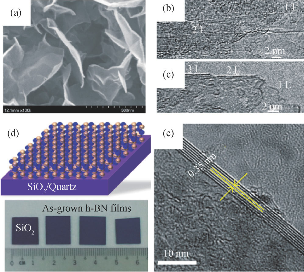
Fig. 12. 2D h-BN synthesized using catalysis-free approaches. (a) SEM images of the BN sheets grown on silicon substrates. High magnification TEM images showing the edges of the BN sheets consisting of 1–2 (b), 1–3 (c) atomic layers, respectively[105]. (d) Schematic diagram (top) and photograph (bottom) of direct grown NCBN films on SiO2/Si substrates. (e) Cross-section TEM image taken at a folded edge showing 7 NCBN layers[106].
Download figure:
Standard image4.2. Other novel methods
A practical problem during the CVD process of h-BN is the use of some unconventional precursors as mentioned above. These compounds are rare and highly toxic, unstable, or pyrophoric. On the other hand, the CVD growth relies on the decomposition of precursors, the rate of which may change dramatically with the exposed surface area of the catalytic substrate; physical vapor deposition (PVD) faces no such constraints. To resolve these problems, some novel approaches such as co-segregation and sputtering deposition method have been developed to synthesize 2D h-BN.
4.2.1. Co-segregation method
Recently, vacuum annealing of nontoxic solid-state precursors has been used to synthesize 2D h-BN. Suzuki et al. reported the simple growth of atomically thin h-BN films on polycrystalline Co or Ni films by annealing a Co (Ni)/amorphous BN/SiO2 structure in vacuum. B and N atoms diffuse through the metal film, although N is almost completely insoluble in both Co and Ni, and precipitation occurs at the topmost surface, as shown in Fig. 13(a)[108]. Further, 2D h-BN thin films were grown by annealing in a vacuum from solid sources deposited on Ni or Co foils. Either a sputter-deposited amorphous BN film or a spin-coated borane ammonia film can be used as the B and N source[109]. Zhang et al. developed a co-segregation method for growing wafer-scale h-BN thin films. Fig. 13(b) shows the sandwiched Fe/(B, N)/Ni substrates. By vacuum annealing, B and N atoms are found to dissolve in the bulk of metals and then co-segregate onto the surface of the growth substrates. The as-grown h-BN thin films was shown in Fig. 13(c)[110]. Interestingly, the h-BN layers were formed on both front and back surface of the metal foils or films using solid sources.
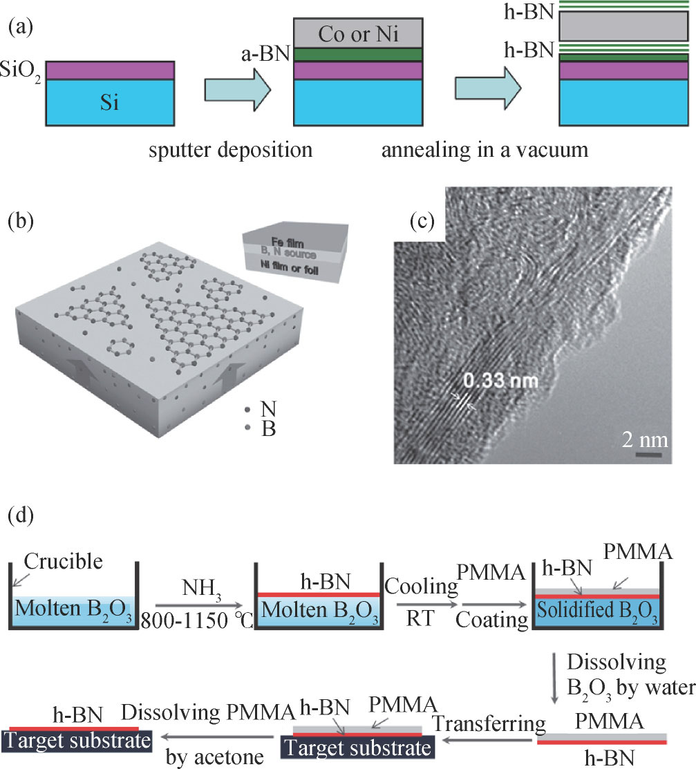
Fig. 13. (a) Schematic of the growth method for a h-BN film by annealing a Co (Ni)/amorphous BN/SiO2 structure in vacuum[108]. (b) Schematic of h-BN synthesis by the vacuum annealing of sandwiched substrates Fe/(B,N)/Ni. (c) High resolution TEM image of a h-BN film edge[110]. (d) Schematic illustration of the self-limiting reaction process of molten B2O3 and gaseous NH3 for h-BN film synthesis and the transference of the h-BN film[112].
Download figure:
Standard imageAdditionally, Nakhaie et al. reported the growth of h-BN films on Ni foils from elemental B and N using molecular beam epitaxy (MBE)[111]. Yang et al. reported a self-limiting growth approach of h-BN based on the interface-controlled self-limiting reaction of molten boron oxide (B2O3) with gaseous ammonia (NH3), as illustrated in Fig. 13(d). An ultrathin h-BN film (20–30 nm) can grow continuously on the entire molten B2O3 surface and then the reaction is stopped spontaneously in a self-terminating manner[112].
4.2.2. Sputtering deposition
To avoid using toxic precursors, Wang et al. reported a simple and innovative method of growing high-quality, few-layer h-BN by ion beam sputtering deposition (IBSD)[113]. By sputtering a benign and nontoxic h-BN target with an Ar ion beam, both triangle and polygonal h-BN domains were achieved on Cu foils, as shown in Figs. 14(a) and 14(b). The domain density of h-BN can be reduced by introducing H2 into the deposition chamber, resulting in an increased size of h-BN domains. By the in situ pretreatment of Ni substrates, as well as by elaborately controlling the growth temperature and the ion beam density, large-sized h-BN domains with the length of side up to 100 μm were grown, as displayed in Figs. 14(c) and 14(d). The synthesized h-BN films were also used to demonstrate applicability for detecting DUV photons[32]. Furthermore, Sutter et al.[114] demonstrated the growth of high-quality, few-layer h-BN on Ru (0001) substrate with controlled thickness by magnetron sputtering of B in N2/Ar. The h-BN films up to two atomic layers were synthesized by reactive deposition at high substrate temperatures. Thicker h-BN films with an arbitrary number of atomic layers are achieved in a two-step process comprising cycles of alternating room temperature deposition and annealing.

Fig. 14. (Color online) Synthesis of 2D h-BN using IBSD. (a) Schematic diagram of the IBSD process. (b) AFM images of h-BN domains grown on Cu foils transferred onto a SiO2/Si substrate[113]. (c) Schematic drawing of the dependence of h-BN domain size on the ion beam density and the growth temperature, from which three regimes can be identified, as indicated by the red dashed lines. (d) SEM images of the h-BN domains prepared on the Ni foils[32].
Download figure:
Standard image5. Summary and future prospects
Two-dimensional h-BN is considered to be an ideal candidate for many applications due to its excellent electrical, thermal and mechanical as well as many other interesting properties. In this paper, we review the recent progress of research on synthesis, properties, and applications of such 2D material. Up to now, a variety of methods have been developed to synthesize 2D h-BN. Similar to graphene, 2D h-BN can be produced by mechanical or chemical exfoliation, nevertheless, the limited domain size hinders their applications in large area devices. CVD is regarded as the most promising method, and it has been reported to synthesize h-BN on a range of transition catalyst metals. However, the CVD process needs to utilize rather unconventional boron-containing precursors. The other novel methods, such as co-segregation and sputtering deposition, have been employed for synthesizing 2D h-BN. Compared to CVD, IBSD growth avoids the use of unconventional precursors and it is also much easier to control, which should be very useful for the large-scale production of h-BN. High-quality, wafer-scale h-BN is urgently required for applications as substrates and dielectric layers and new synthesis approaches need to be developed. However, there is still a long way to go to improve novel synthesis techniques. To a large degree, the widespread applications of 2D h-BN are dependent on progress in the synthesis of 2D h-BN with controlled domain size, morphology, and layer number. This seems to remain a major challenge for the next few years. Recently, both in-plane and stacked graphene/h-BN heterostructures have been investigated theoretically and experimentally, in the interest of combining their complementary properties for use in a wide range of applications. Thus, more attention should be paid to the development of graphene/h-BN heterojunctions in the future. It is anticipated that continuing achievements in synthesizing high-quality h-BN layer will soon enable the realization of electronic devices based on graphene/h-BN heterojunctions.
Footnotes
- *
Project supported by the National Natural Science Foundation of China (Nos. 61376007, 61674137) and the National Key Research and Development Program of China (No. 2016YFB0400802).