
Abstract
Many applications in proteomics and lab-on-chip analysis require methods that guide proteins to assemble at surfaces with high spatial and temporal control. Electrical inputs are particularly convenient to control, and there has been considerable effort to discover simple and generic mechanisms that allow electrical inputs to trigger protein assembly on-demand. Here, we report the electroaddressing of a protein to a patterned surface by coupling two generic electroaddressing mechanisms. First, we electrodeposit the stimuli-responsive film-forming aminopolysaccharide chitosan to form a hydrogel matrix at the electrode surface. After deposition, the matrix is chemically functionalized with alkyne groups. Second, we ''electro-click' an azide-tagged protein to the functionalized matrix using electrical signals to trigger conjugation by Huisgen 1,3-dipolar cycloadditions. Specifically, a cathodic potential is applied to the matrix-coated electrode to reduce Cu(II) to Cu(I) which is required for the click reaction. Using fluorescently-labeled bovine serum albumin as our model, we demonstrate that protein conjugation can be controlled spatially and temporally. We anticipate that the coupling of polysaccharide electrodeposition and electro-click chemistry will provide a simple and generic approach to electroaddress proteins within compatible hydrogel matrices.
Export citation and abstract BibTeX RIS
Introduction
The assembly of proteins at electrode surfaces offers the broad potential for coupling the molecular recognition properties of biology with the signal transduction capabilities of electronics. For instance, the success of home-use glucose monitoring devices suggests even broader possibilities for multiplexed biosensing in handheld devices for applications that range from the detection of contaminants on-site to the diagnosis of diseases at the point-of-care. To realize this potential, simple mechanisms are required to assemble proteins at the electrode address and to provide these assemblies with microenvironments that protect these labile biological components. Here, we couple two particularly attractive approaches: we electroaddress our protein using electrode-imposed signals and incorporate our protein within a polysaccharide-based hydrogel matrix.
Several mechanisms have been reported for the electroaddressing of proteins and these involve either molecular linkages or incorporation into thin polymer film. Proteins modified with diazonium can be directly electro-addressed at the surface of the graphite electrodes [1]. One approach for covalent connection for proteins relates to the electrochemical reaction of moieties on the electrode surface. For instance, electrochemical reactions convert inert nitro substituents into reactive amines [2]. In another study, hydroquinones have been converted into benzoquinones that can react with proteins [3, 4]. Another strategy is to incorporate proteins into thin films and this has been accomplished either by the electropolymerization of monomers to generate conductive films (e.g. polyaniline [5], polypyrrole [6], or polyphenols [7]) or by co-deposition with stimuli-responsive polymers [8–11].
Polysaccharides and hydrogels are commonly believed to provide compatible microenvironments for labile biological components (e.g., proteins and cells) [12–15]. Over the last decade, mechanisms were discovered for the electrodeposition of several stimuli-responsive hydrogel-forming polysaccharides. Initial studies demonstrated deposition of the aminopolysacchraide chitosan through a neutralization mechanism in which electrochemically-generated pH-gradients at the cathode are used to trigger a sol–gel transition of this weak polyelectrolyte [16–21]. Later studies demonstrated an analogous neutralization-based mechanism for electrodepositing the acidic polysaccharide alginate at the anode [22–24]. These studies prompted additional studies on alternative mechanisms for polysaccharide electrodeposition [25]. A mechanism was discovered for the anodic deposition of chitosan hydrogels and this mechanism involves a chemical modification of chitosan that leads to the formation of a covalently cross-linked chemical gel [26].
Chitosan is unique for accessibility of reactive amine groups for protein conjugation and recognition to localized electrical signals, supported by its pH responsive (pKa 6.3) and film forming properties. Previous research has shown chitosan deposition provides a versatile platform for protein assembly either on micropatterned chips or in pre-packaged bioMEMS [27–32]. Proteins can be codeposited within chitosan film or can react with active substituents on prior deposited chitosan film with spatial-selectivity and quantitative-control. Thus, chitosan provides an interface between microelectrodes and biological components. Significantly, the integration of biological components with deposited chitosan on bioMEMS devices provides functionalization for biosensing, enzymatic catalysis and specific biorecognition [33].
Here, we employ chitosan electrodeposition to create a hydrogel matrix and then electroaddress a protein to this matrix using an 'electro-click' method as illustrated in scheme 1. It is well known that 'click' chemistry provides an efficient and mild mechanism to conjugate proteins [34–36]. The Cu(I) catalyzed azide-alkyne cycloaddition has been well studied for surface conjugation of a wide variety of organic, polymeric, and biological molecules [37–41]. Previous studies reported the functionalization of conducting polymers by 'click chemistry' in which the Cu(I) catalyst was generated electrochemically [42–44]. In this study, we extend the 'electro-click' chemistry to non-conducting polymer modified electrodes. As shown in scheme 1, we use three steps to address proteins to a patterned surface; (i) cathodic electrodeposition of a chitosan hydrogel, (ii) chemical-functionalization of the electrodeposited chitosan with alkyne groups, and (iii) cathodic reduction of Cu(II) to Cu(I) to initiate the click coupling reaction between the alkyne-functionalized chitosan and an azide-tagged protein.
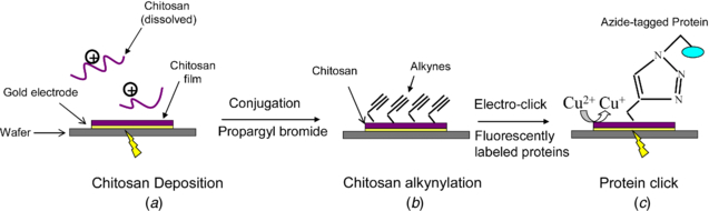
Scheme 1. Illustration for protein addressing by 'electro-click'. (a) Chip with patterned gold electrode deposited with chitosan. (b) Further conjugation of the deposited chitosan film with alkynes. (c) Protein addressing to chitosan by 'electro-click' in which the produce of Cu(I) that catalyzes the click reaction was controlled by an electrical potential.
Download figure:
Standard image High-resolution imageMaterials and methods
Chitosan from crab shells (85% deacetylation and 200 kDa, as reported by the supplier), Alexa Fluor 488 Azide, bovine serum albumin (BSA) and fluorescent isothiocyanate (FITC) were purchased from Sigma-Aldrich; Dylight 550 NHS ester was purchased from Thermo Fisher Scientific Inc.; propargyl bromide was purchased from Shanghai Darui fine chemical company; NHS-dPEG(4)-N3 (NHS and N3 was connected by 4 polyethylene glycol linker) was purchased from Quanta Biodesign; all other chemicals were purchased from Shanghai Sinopharm Chemical Reagent Co., Ltd.
Silicon wafers previously coated with 1 µm thermal oxide film were deposited with 90 Å thick chromium (Cr) and then 2000 Å thick gold (Au) films. Patterned electrode chips were prepared using standard photolithographic methods, as previously described [45]. The chip with two electrically-independent gold rectangular patterns (8 mm × 1 mm) separated by a 1 mm space was used in this study.
A chitosan solution (1.0 w/v%, pH 5.5) was used for electrodeposition. Chitosan was dissolved in dilute HCl and the pH was adjusted to 5.5 by 1 M NaOH. Electrodeposition was performed by connecting the chip to a power supply (CHI 624D, Shanghai). The chip used as a cathode and a platinum foil used as an anode were partially-immersed in chitosan solution and a constant voltage (3.0 V) was imposed for 5 min. Under this voltage, a typical current of 30–60 µA was observed. The deposited chitosan film (thickness ∼10 µm) on patterned chip was air dried for further usage.
For conjugation of BSA to chitosan film, BSA was labeled with azide tag. The labeling was performed by incubating BSA (0.2 mg/ml) in 4% NaHCO3 with NHS-dPEG(4)-N3 (molar ratio of BSA to NHS-dPEG(4)-N3 was 2:1) for 4 h. In order to visualize protein conjugation to chitosan, BSA was further labeled with fluorescent probes. FITC or DyLight 550 NHS ester dissolved in DMSO was added slowly to azide-tagged BSA solution (molar ratio of BSA to fluorescent probes was 1.0) and the mixture was kept at 4 °C for 8 h. The labeling was stopped by adding NH4Cl with a final concentration of 50 mM. Finally, the resulting BSA solution was dialyzed in dark at 4 °C for 1 week to remove any unreacted labeling reagent.
The alkynylation of chitosan film on chip was performed by immersed the chip in a 10 ml mixture of NaOH (4 mol l−l) and isopropyl alcohol (4:1; V/V), and the reaction was initiated by adding propargyl bromide (50 µl). The chip was allowed to incubate in the solution for 5 h at 60 °C. After the reaction, the chip was washed extensively with ethanol.
The conjugation of BSA to deposited chitosan on chips was realized by 'click chemistry'. After the alkynylation of chitosan film on the chip, the chip was immersed in 2 ml phosphate buffer solution (0.1M PBS, pH 7.0) containing Alexa Fluor 488 Azide. A solution (25 µl) containing CuSO4 (4 mmol l–1), ascorbic acid (20 mmol l−1), EDTA(1 mmol l–1) was added to above mentioned phosphate buffer (2 ml) to catalyze the click reaction. In some experiments, the reduction of Cu(II) to Cu(I) was initiated by electrochemical method. For this, the chip was connected to an electrochemical workstation (CHI 624D, Shanghai) with a platinum wire as counter electrode and an Ag/AgCl wire as a reference electrode. The electrodes were partially immersed in a phosphate buffer with FITC or DyLight 550 NHS ester labeled azide-tagged BSA (12.5 µg ml−1), CuSO4 (3 mmol l−1) and NaNO3 (10 mmol l−1). A cyclic voltammogram was performed between 500 and −300 mV at a scan rate of 250 mV s−1 for 10 min. Then the chip was removed from the solution and washed with phosphate buffer containing 0.1% Tween for three times (10 min for each wash). The conjugation of BSA on the chip was examined by a fluorescence stereomicroscope (MZX80, Mshot).
Results and discussion
To conjugate chitosan with alkynes, we functionalize the amino groups of chitosan through halogenation. Firstly, we electrodeposited chitosan (1.0%, pH 5.5) onto the gold coated wafer and incubated the wafer in a mixture of NaOH and isopropyl alcohol containing propargyl bromide at 60 °C for 5 h. After the alkynylation of chitosan, the wafer was rinsed extensively with ethanol. The pale yellow film was peeled off from the wafer and subjected to FT-IR study. As illustrated in figure 1(a), the alkyne substitution occurs primarily on NH2 moieties because of the high nucleophilic property of amino groups [46]. The FT-IR spectra of chitosan and alkynylated chitosan, as shown in figure 1(b), provide the evidence for alkyne substitution. In the spectrum of unmodified chitosan, the characteristic peaks at 3435 cm−1, 1651 cm−1 and 1598 cm−1 are assigned to hydroxyl, amide and amino groups, respectively, consistent with the deposition of chitosan on the electrode. The appearance of a peak at 2120 cm−1 on alkynylated chitosan corresponds to alkyne group absorption [47]. It should be noted that a strong peak appears at 1400 cm−1, which can be assigned to the vibration of newly formed –C-N. The FT-IR analysis suggests the deposition of chitosan on the wafer and its conjugation of alkynes on amino groups.
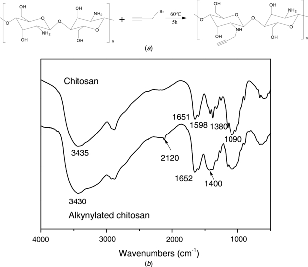
Figure 1. The alkynylation of chitosan film. (a) Schematic illustrating of the reaction of chitosan with propargyl bromide. (b) FT-IR spectra of chitosan and alkynylated chitosan.
Download figure:
Standard image High-resolution imageWe next examined the selectivity of click reaction on alkynylated chitosan using a patterned chip as the experimental approach illustrated in figure 2(a). Specifically, chitosan was deposited on the left electrode of the patterned chip (figure 2(b)) and functionalized with alkyne groups using procedures described above. Next the right electrode of the chip was electrodeposited with chitosan. The chip was incubated in a phosphate buffer containing Alexa Fluor 488 Azide, which is a fluorescently labeled azide molecule to visualize the assembly; then a phosphate buffer solution containing Cu(II), ascorbic acid and EDTA was added to catalyze the click reaction. The conjugation of Alexa Fluor 488 Azide on the patterned chip was examined using fluorescence microscopy. The fluorescence photomicrograph and image analysis of figure 2(b) show that fluorescence is predominantly confined to the left electrode where the deposited chitosan was functionalized with alkynes. This result indicates the click reaction is selective for alkynylated chitosan.
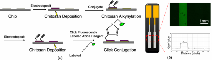
Figure 2. Selective assembly of azide reagent to patterned chip. (a) Schematic of the experiment to test the assembly of azide reagent to alkynylated chitosan. (b) Schematic of patterned chip with two separate electrodes and fluorescence photomicrograph with corresponding fluorescence intensity profile showing fluorescently labeled azide reagent is assembled onto the left electrode (with alkynylated chitosan) and minimal non-specific binding to the control chitosan electrodeposited on the right electrode.
Download figure:
Standard image High-resolution imageNext we demonstrated the assembly of azide-tagged BSA on chitosan by click chemistry was triggered by electrical signals as illustrated in figure 3(a). In order to track the BSA assembly, we further labeled azide-tagged BSA with FITC for fluorescence observation. We electrodeposited chitosan on the patterned chip and functionalized chitosan with alkyne groups. The chip, which served as the working electrode, was partially immersed in a phosphate buffer with FITC labeled azide-tagged BSA, Cu(II) and NaNO3, and connected to a three electrode system. Initial cyclic voltammetry study for Cu(II) reduction at chitosan coated gold electrode suggests the voltage range of 500 to −300 mV. After cyclic voltammogram circulation for 10 min, the chip was washed by phosphate buffer containing Tween (three washes each for 10 min) to remove physically-bonded BSA. For comparison, the chip with chitosan deposition with no alkyne functionalization was treated with the same procedure. The chips were examined using fluorescence microscopy and pictures were taken at the same exposure time. The fluorescence photomicrographs in figure 3(b) shows strong fluorescence on the two electrodes deposited with chitosan and functionalized with alkyne groups, and the fluorescence intensity of each of these electrodes was similar. In contrast, there is less and inhomogeneous fluorescence on the control electrodes in which chitosan was electrodeposited by not functionalized with alkyne groups. Presumably the fluorescence observed on these control electrodes is due to non-specific protein binding to the chitosan films. The results in figure 3(b) indicate that azide-tagged protein conjugation is triggered by the imposed electrical inputs. Further, the image analysis in figure 3(b) indicates that the coupling of chitosan electrodeposition and electro-click chemistry enables protein addressing at separate electrodes to be performed in parallel.
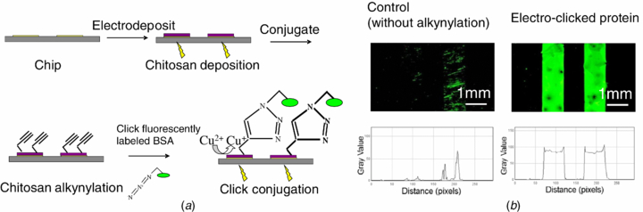
Figure 3. Parallel protein addressing to deposited chitosan film by 'electro-click'. (a) Schematic of experiment. (b) Fluorescently labeled BSA addressing to chip by click chemistry controlled by electrical potential. Fluorescence photomicrographs with fluorescence intensity profile showing fluorescently labeled BSA is assembled onto the chip with alkynylated chitosan (the right) while little non-specific assembly on the chip with chitosan (the left, as control).
Download figure:
Standard image High-resolution imageFinally, we demonstrated sequential click conjugation of azide-tagged BSA to separated electrodes by imposed electrical signals as illustrated in figure 4(a). Using methods described above we electrodeposited chitosan on the two electrodes. Next, we functionalized the chitosan with alkynes by incubating the chip in a solution containing propargyl bromide. Then the chip was partially immersed in DyLight 550 labeled azide-tagged BSA and a cyclic voltammogram circulation was imposed to the left electrode at 500 to −300 mV for 10 min. The fluorescence image in figure 4(b) shows red fluorescence on the left electrode with voltage biased, while there is little fluorescence on the right electrode without potential imposed. We then performed the second protein conjugation step with FITC labeled azide-tagged BSA onto the right electrode using a similar electrochemical procedure. The right image in figure 4(b) shows the appearance of green fluorescence on the right electrode. These results indicate that protein can be 'electro-clicked' to deposited chitosan films and this electroaddressing approach can be controlled spatially and temporally.

Figure 4. Sequential addressing of fluorescently labeled azide-tagged BSA by 'electro-click'. (a) Schematic of experiment showing electrical signal guided sequential protein click conjugation on separated electrodes. (b) Fluorescence photomicrographs with fluorescence intensity profile showing the progressive fluorescently labeled azide-tagged BSA assembly.
Download figure:
Standard image High-resolution image
This proof-of-principle study demonstrates the electroaddressing of proteins by coupling chitosan electrodeposition and electro-click chemistry. While we did not specifically examine protein activity, we should note that both chitosan electrodeposition [48, 49] and click conjugation [50, 51] have become rather routine methods for assembling biologically-active proteins.
Conclusion
In conclusion, this study demonstrates protein electroaddressing by coupling polysaccharide electrodeposition with electrically-induced click chemistry. This approach involves; electrodeposition of the pH-responsive amino polysaccharide chitosan to create a hydrogel matrix, functionalization of chitosan's amino group with alkyne moieties, and initiation of conjugation by the cathodic reduction of Cu(II) to Cu(I) to catalyze the coupling of azide-tagged proteins to alkynylated chitosan. This on-demand protein conjugation approach is performed under mild conditions in aqueous solution, and is achieved with spatial and temporal control. We anticipate that this on-demand electroaddressing approach should provide an efficient, stable and generic approach for integrating biological components into electronic devices (e.g., for lab-on-a-chip devices).
Acknowledgments
The authors gratefully acknowledge financial support from National Natural Science Foundation of China (grant no 21007049), Program for New Century Excellent Talents in University (NECT-10-0618), Natural Science Foundation of Hubei Province of China (grant no 2011CDB268), Large-scale Instrument and Equipment Sharing Foundation of Wuhan University, and DTRA (W91B9480520121).