

Abstract
This work presents studies of plasmonic silver nanoparticles (AgNPs) formation at low temperatures (200 °C–300 °C) onto Si surface by sputtering followed with rapid thermal processing (RTP) for different time durations(5–30 min). The study reveals that 20 min RTP at all temperatures show minimum average size of AgNPs (60.42 nm) with corresponding reduction in reflectance of Si surface from 40.12% to mere 1.15% only in wavelength region 300–800 nm for RTP at 200 °C. A detailed supporting growth mechanism is also discussed. This low temperature technique can be helpful in achieving efficiency improvement in solar cells via reflectance reduction with additional features such as reproducibility, minimal time and very good adhesion without damaging underlying layers device parameters.
Export citation and abstract BibTeX RIS

Original content from this work may be used under the terms of the Creative Commons Attribution 3.0 licence. Any further distribution of this work must maintain attribution to the author(s) and the title of the work, journal citation and DOI.
1. Introduction
Global photovoltaic (PV) installation is forecasted to grow at a rate of 13% and may reach up to 64.7 GW in 2016 surpassing its previous year 2015 forecast of 57.8 GW [1]. Amongst all solar PV technologies, the silicon (Si) based technology share 93% of total production in year of 2015 [2]. Typical Si solar cells have thickness of 180–300 µm and the cost of the cells mainly increases due to the cost of the base Si material and its fabrication technologies. In order to scale back the cost value, thin film PV cells are getting more popularity among research and business applications. Thin film solar cells with thickness range (~1–2 µm) can be deposited on low cost substrates like glass, plastic or stainless steel and so has the potential to drastically cut-back the cost of PV cells [3]. But, the major drawback for these thin film solar cells are its low light absorption capacity as compared to wafer based solar cells due to its leaner geometry which diminishes its efficiency [4]. In conventional Si solar cells, trapping of light is usually achieved using a pyramidal textured surface (~10 µm) that causes scattering of light into the solar cell, increasing its effective path length in the cell which is not possible in thin film solar cells due to its thinner geometry [5]. Also this surface texturing leads to increase in recombination losses attributable to excess area [6]. Light trapping mechanism using surface plasmon resonance phenomenon in metallic nanoparticles (NPs) can be devised in thin film solar cells to come up with additional electron–hole pair by increasing its light absorption from scattered light and consequently can further enhanced its efficiency. In order to utilize the advantages of plasmonic phenomenon using metallic NPs for light trapping in thin-film solar cells, three different mechanisms have been suggested and discussed by Atwater et al [7]. The first of these mechanisms includes the formation of NPs on the top surface of the solar cells, whereas the second mechanism includes NPs being embedded directly into the active layer of the semiconductor material and the third one consists of rectangular nanostructures (like grating) on the back surface of the solar cells.
Many research groups have already suggested AgNPs as plasmonic layer on Si surface to increase the efficiency of Si based solar cells [8–10]. Recently AgNPs as plasmonic layer on textured Si surface has been investigated and achieved an enhancement in Si solar cell efficiency by the way of increasing photocurrent [11]. AgNPs arrangement can be generated on Si surface by rapid thermal heating of thin film using rapid thermal annealing/rapid thermal processing (RTA/RTP). The benefits of using RTA/RTP can be easily integrated into the already existing Si solar cell fabrication plants systems which allow creation of metal plasmonic layer with minimal time period. Recently a research group was able to generate Ag NPs arrangement on Si surface using RTP in high temperature such as 800 °C [12]. But this high temperature annealing of Si solar cells in fabrication line can adversely affect device parameters and also increases the thermal budget of the process line [13, 14]. Therefore, Ag NPs as plasmonic layer deposited by RF sputtering at room temperature followed with RTP heat treatment in low temperature regime ~200 °C can be very effective in solar cell device fabrication as the technique has reproducibility, improves adhesion and does not affect other device parameters [15]. In this work plasmonic AgNPs are explored on top surface of polished single crystalline Si (c–Si) substrate using RTP in low temperature range. Also, the mechanism for the formation of plasmonic AgNPs on c–Si surface at low temperature is discussed in detail. The so-formed plasmonic AgNPs arrays are used to reduce the reflectance for effective light scattering in order to increase the optical path length of Si solar cells.
2. Experimental
Plasmonic AgNPs on (1 0 0) c–Si substrate were created using radio frequency (RF) sputtering (model: HHV—12'' MSPT, 13.56 MHz) and then annealed by RTP (model: MTI-EQ-OTF-1200X-4-RTP-HV). After cleaning c–Si p-type substrate with acetone, propanol and deionized (DI) water, the substrates are kept for thin film deposition by RF sputtering which had silver target with 99.999% purity. The base pressures and growth pressure in the sputtering unit were 2.6 × 10⁻⁶ mbar and 6 × 10⁻² mbar, respectively, with argon gas released into the chamber at a constant pressure of 2 kg-f cm−2 during film deposition process. The deposition was carried out at room temperature and distance between targets to substrate was 2 inches. After several depositions in RF sputtering unit, power rate of 75 W for 10 s is optimized for silver thin film deposition on the c–Si substrate. The post deposition heating of silver thin film by RTP with heating rate of 100 °C s−1 was carried out at temperatures of 200 °C, 250 °C, and 300 °C in vacuum with chamber less than 4 mtorr for a time interval of 5 min, 10 min, 15 min, 20 min and 30 min. After annealing by RTP, the samples were cooled naturally to room temperature conditions and resulted into formation of AgNPs of various sizes with different arrangements.
The surface morphology of various AgNPs layers were characterized by scanning electron microscope (SEM) (Zeiss—EVO-18) and field emission electron microscopy (FESEM) (TESCAN-MIRA). The absorption and reflectance spectra of prepared samples were recorded by UV–Vis spectrophotometers (Shimadzu UV-2600 and Shimadzu ISR-2600 plus integration sphere, respectively). An image processing software ImageJ v1.45 was used to calculate the average size of the prepared AgNPs [16].
3. Results and discussions
3.1. Absorbance study
In order to confirm the plasmonic behavior of AgNPs by RTP, Ag thin film was deposited on cleaned glass substrate by sputtering followed with RTP at 250 °C under the conditions mentioned in above experimental details. Plasmonic AgNPs layer generation using RTP at 250 °C temperature for different time intervals (5–30 min) onto glass is confirmed by absorbance spectra as shown in figure 1. AgNPs show plasmonic behavior with two peaks in absorbance spectrum. The primary peak at around 450 nm is responsible for surface plasmon resonance while secondary peak at around 360 nm is responsible for quadruple resonance. The plasmonic peak position of silver can be varied by tuning the size, shape and material of the nanoparticle as well as depends on the dielectric medium surrounding the particle [17, 18]. Figure 1 clearly shows plasmon peak for samples 1, 2, 3, 4 and 5 at 463.5 nm, 453.38 nm, 447.5 nm, 452.9 nm and 453.1 nm, respectively, with particle sizes 107.6 nm, 104.5 nm, 85.1 nm, 88.5 nm and 96.1 nm, respectively. A blue shift of plasmon resonance peak along with decrease in AgNPs sizes is observed from 5 min to 15 min RTP. A red shift is started from 20 min to 30 min RTP with increase in Ag NPs size with respect to 15 min RTP. The secondary plasmon peak in each absorbance spectrum observed around 360 nm can be attributed to quadruple resonance [18].

Figure 1. Absorption spectra of various size AgNPs onto glass substrate.
Download figure:
Standard image High-resolution image3.2. Surface study
The surface morphology of as deposited Ag thin film on c–Si (1 0 0) substrate is characterized by SEM and FESEM measurements and are shown in figure 2. The figure 2(a) shows nonvisibility of surface features in SEM image therefore FESEM measurement (figure 2(b)) was done at higher magnification and resolution which depicts non-continuous Ag thin film with flattened particles arrangement.
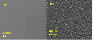
Figure 2. SEM and FESEM images of as deposited Ag thin film on c–Si (1 0 0) surface by RF sputtering at (a) ×50 000 and (b) ×150 000 magnifications.
Download figure:
Standard image High-resolution imageFigures 3(a)–(e), figures 4(a)–(e) and figures 5(a)–(e) show SEM images depicting effect of RTP time duration (5, 10, 15, 20 and 30 min) and temperature (200 °C, 250 °C and 300 °C) for fabrication of AgNPs layer on polished c–Si substrate. Figures 3–5 show variation in surface morphology of formed AgNPs for different annealing durations of 5, 10, 15, 20 and 30 min and confirms that the average particles size of AgNPs is decreasing from 5 min to 20 min RTP durations and minimized for 20 min annealing in respective annealing temperatures as shown in figures 3(f), 4(f) and 5(f). Further rise in RTP duration to 30 min shows increase in average particle size at respective variable temperatures in all the figures 3–5. The shape of AgNP is found to be asymmetrical on increasing RTP temperature. Lowest average AgNPs with size of 60.42 nm is observed for 20 min RTP of Ag thin film at 200 °C.

Figure 3. SEM images of AgNPs arrangement for variable RTP durations of (a) 5 min, (b) 10 min, (c) 15 min, (d) 20 min, (e) 30 min and (f) average particle size variation with RTP duration at 200 °C.
Download figure:
Standard image High-resolution image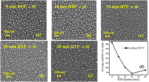
Figure 4. SEM images of AgNPs arrangement for variable RTP durations of (a) 5 min, (b) 10 min, (c) 15 min, (d) 20 min, (e) 30 min and (f) average particle size variation with RTP duration at 2500 °C.
Download figure:
Standard image High-resolution image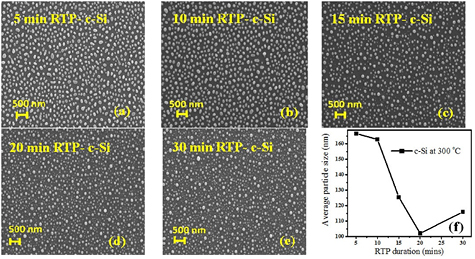
Figure 5. SEM images of AgNPs arrangement for variable RTP durations of (a) 5 min, (b) 10 min, (c) 15 min, (d) 20 min, (e) 30 min and (f) average particle size variation with RTP duration at 300 °C.
Download figure:
Standard image High-resolution imageThe average particle size variation with RTP duration at temperatures 200 °C, 250 °C and 300 °C are shown in figures 3(f), 4(f) and 5(f), respectively. The calculated average particle sizes from SEM images are summarized in table 1.
Table 1. Calculated average particle size of AgNPs.
| RTP temperature (°C) | RTA duration and shape with size (nm) | ||||
|---|---|---|---|---|---|
| 5 min | 10 min | 15 min | 20 min | 30 min | |
| 200 | 90.96 | 81.91 | 77.16 | 60.42 | 79.42 |
| 250 | 153.25 | 123.35 | 100.92 | 88.1 | 95.12 |
| 300 | 166.65 | 162.82 | 125.52 | 102.15 | 115.95 |
Thus SEM studies reveal that AgNPs sizes in irregular arrangement are decreasing with increase of RTP duration and minimized for 20 min RTP at temperatures 200 °C, 250 °C and 300 °C.
The changes in surface morphology of AgNPs due to RTP at different temperatures for various time durations can be explained by considering thin film growth mechanism. A typical thin film growth processes consists of several steps like adsorption, cluster formation, surface diffusion, desorption, nucleation, lateral growth leading to island formation, agglomeration of the island for coalescence and then filling of channels and holes in porous network of coalescence particles which can result into a continuous film [19–21].
As deposited silver thin film on Si surface by RF sputtering has intrinsic stress and found to be compressive in nature [22]. Zhao et al [23] and Liu et al [24] explored AgNPs array formation by annealing at temperature 400 °C and 300–800 °C, respectively, of Ag thin film deposited by thermal evaporation and dealt in detail the surface plasmonic behavior for solar cell applications. Though these research groups attributed various AgNPs formations in this methodology to supplied thermal energy, surface tension, thermal diffusion and recrystallization processes but reported literature lacks detailed explanation of systematic formation of AgNPs. Based on reported literature, a growth mechanism of AgNPs formation by RTP annealing of Ag thin film is discussed in detail in this report. In our case, rapid thermal heating provide thermal energy to the Ag particles onto Si surface. On increasing annealing time, atomistic mobility increases and so surface diffusion start increasing. The additional thermal energy imparted to Ag particles during annealing leads to recrystallization which occurs by nucleation and growth during solid state reaction [25]. On increasing RTP annealing time further coalescence amongst particles can be observed driven by higher surface diffusion. Upon cooling of this heat treated non-continuous Ag film on Si surface to room temperature, mismatching in thermal expansion coefficient of substrate (c–Si) (3.52 × 10⁻⁶ K−1 at 200 °C) and sputtered thin metallic Ag film (19 × 10−6 K−1) leads to shrinkage in thin film and so compressive stress exists at the interface of thin film and c–Si substrate due to mismatching in thermal expansion coefficient which results into the formation of plasmonic AgNPs on c–Si substrate. Here annealing temperature and annealing time also play important role in determining ultimate shape, size and interparticle distance amongst Ag NPs. Since c–Si substrate and Ag have 'fcc' structures and has no appreciable lattice mismatching [26, 27], therefore change in nature of stress due to chemical nature and surface topography of substrate can be ignored. If a thin film at temperature Ta is cooled to room temperature Tr, the existing thermal stress force (Ff) acting at the interface of thin film and substrate can be calculated by [28]

where w is width of substrate, df is thickness of the film, ds is thickness of substrate, αs is thermal expansion coefficient of substrate, αf is thermal expansion coefficient of film (Ag), Ta is annealing temperature, Tr is room temperature, νf is Poisson's ratio of film, νs is Poisson's ratio of substrate, Ef is Young's modulus of film, Es is Young's modulus of substrate.
Since in our case  is very smaller than
  , therefore thermal stress in the film is

Based on available literature, the thermal expansion coefficient of silver is 19 × 10−6 K−1 [29] and that of Si substrate are 3.52 × 10⁻⁶ K−1, 3.72 × 10⁻⁶ K−1 and 3.84 × 10⁻⁶ K−1 at temperature 200 °C, 250 °C and 300 °C, respectively [30]. Young's modulus of elasticity and Poisson's ratio of silver film [31] are 82.5 GPa and 0.364, respectively. The calculated compressive stress (using equation (2)) has magnitudes 0.347 GPa K−1, 0.442 GPa K−1 and 0.537 GPa K−1 at temperatures 200 °C, 250 °C and 300 °C, respectively. At 200 °C RTP temperature, Ag thin film results into AgNPs cluster formation for 5 min RTP. On further increase in RTP annealing time, residual stress relaxation takes place in thin film. New grain formation during recrystallization process usually occurs with decreases in average AgNPs size with the increase of annealing time [25]. The average AgNPs size reduction from 10 to 15 min RTP at each temperature during recrystallization can be attributed to degree of recrystallization and then minimum average AgNPs particle size is achieved for 20 min RTP at each temperature. Heat treatment during RTP results into residual stress relaxation with recrystallization amongst AgNPs and so energy minimization takes place for 20 min RTP which results into decrease in surface area of AgNPs. Further increase in RTP duration to 30 min results into enhanced surface diffusion which leads to particles agglomeration and results into island formation due to coalescence. Similar trends are observed for variable RTP duration at 250 °C and 300 °C as listed in table 1. At constant RTP duration of 5 min with the increase in RTP temperature, Ag NPs cluster size increases (table 1) due to increased strain energy. Similar trends are observed for each constant RTP duration with the variation of temperature from 200 °C to 300 °C as listed in table 1. Thus RTP time, RTP temperature and so generated thermal stress, surface diffusion play vital role in determining ultimate size of Ag NPs on Si substrate.
In order to understand effect of RTP temperature on AgNPs sizes, a graph between average size of Ag NPs and RTP temperature for constant RTP duration is summarized in figure 6. A larger increase in average size of Ag NPs is observed for 5 min RTP from 200 °C to 250 °C which becomes less significant for further increase in temperature from 250 °C to 300 °C. For 10 min RTP, the increase in average Ag NPs size is constant for the rise of temperature from 200 °C to 300 °C. This increase in average Ag NPs sizes decreases with temperature for 15 and 20 min RTP. The increase in average Ag NPs is minimum for 30 min RTP. Thus highest increase in average Ag NPs size with temperature in the range of 200 °C–300 °C is observed for 10 min RTP while it becomes minimum for 30 min RTP.
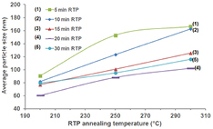
Figure 6. Average AgNPs size variation with respect to RTP temperature.
Download figure:
Standard image High-resolution imageFigure 7 shows summary of effect of RTP time durations on average AgNPs sizes at constant temperatures.

Figure 7. Average AgNPs size variation with respect to RTP time in minutes.
Download figure:
Standard image High-resolution image3.3. Reflectance study
The reflectance measurements of AgNPs on c–Si substrate in wavelength region 300–800 nm at constant RTP temperature for different RTP time duration are shown in figure 8 (at 200 °C), figure 9 (at 250 °C) and figure 10 (at 300 °C).The reflectance spectra clearly indicate highly reflective Ag thin film onto c–Si substrate due to highly packed flattened particles as shown in figure 2(b). After performing RTP of non-continuous silver thin films at constant temperature, average reflectance drops drastically due to creation of isolated AgNPs array as plasmonic layer. The appreciable change in reflectance of polished c–Si wafer due to surface plasmonic AgNPs may be attributed to the changes in size of AgNPs by RTP. It has been observed that in the typical samples, the average reflectance (for 5 min RTP at 200 °C) from around 19.38% is reduced up to 1.15% (for 20 minRTP at 200 °C). The tuning of AgNPs size at 200 °C RTP show negligible reflectance in long wavelength region (600–800 nm) and so can be efficiently utilize for significant photocurrent enhancement in Si based solar cell devices. This significant reflectance reduction for 20 min RTP can be attributed to the fact that the formation of NPs are more distinctly spaced and spherical in appearance to acquire energy minimization during RTP which favors appreciable forward scattering [32]. Moreover, dominant short wavelength (~350 nm) reflectance reduction with AgNPs size at 200 °C and 300 °C may be attributed to the quadruple resonance [32]. The effects of RTP duration with average reflectance are summarized in figure 11 at constant temperature. Figure 11 indicates maximum average reflectance reduction for 20 min RTP for all annealing temperatures due to minimum average size of AgNPs which may be attributed to relatively more spherical shape of particles. The effect of RTP temperature on average reflectance for constant RTP durations is summarized in figure 12. On increasing RTP temperature from 200 °C to 250 °C, reflectance decreases for 5 and 10 min RTP. Further rise in RTP temperature to 300 °C, reflectance increases for all RTP time durations.

Figure 8. Reflectance spectrum of RTP treated AgNPs onto Si surface at 200 °C.
Download figure:
Standard image High-resolution image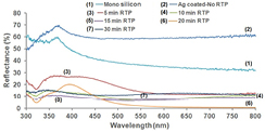
Figure 9. Reflectance spectrum of RTP treated AgNPs onto Si surface at 250 °C.
Download figure:
Standard image High-resolution image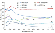
Figure 10. Reflectance spectrum of RTP treated AgNPs onto Si surface at 300 °C.
Download figure:
Standard image High-resolution image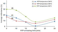
Figure 11. Comparative average reflectance of AgNPs onto Si surface with respect to RTP durations.
Download figure:
Standard image High-resolution image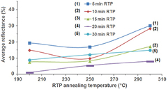
Figure 12. Comparative average reflectance of AgNPs onto Si surface with respect RTP temperature.
Download figure:
Standard image High-resolution image
Thus tuning of AgNPs size is observed due to RTP temperatures and durations which can be an effective way to design reflectance reduction of Si surface.
4. Conclusions
The silver thin film deposition by sputtering followed with various RTP time durations in low temperatures region (200 °C–300 °C) has resulted into arrangements of plasmonic AgNPs of different sizes onto Si surface upon cooling to room temperature. The proposed growth mechanism suggests that acting thermal stress results into formation of AgNPs cluster after cooling of RTP treated Si surface. On increasing RTP time, degree of recrystallization determines variation in shape and sizes of AgNPs and leads to minimize surface area of AgNPs for 20 min RTP at all temperature. On increasing RTP time further dominant surface diffusion leads to agglomeration and so results into island formation of AgNPs. In this work, average AgNPs size reductions occur from 5 to 20 min RTP and then size increment of NPs is observed for 30 min RTP in all temperatures. For 20 min RTP at 200 °C, 250 °C and 300 °C, maximum reflectance reduction amongst all RTP durations may be attributed to relatively more spherical AgNPs which can enhance forward scattering. Amongst 20 min RTP at different temperatures, the heat treatment at 200 °C temperature show significant average reflectance reduction from 40.12% to mere 1.15% only in 300–800 nm wavelength region. Hence, this work suggests that low temperature technique for formation of AgNPs as plasmonic layer on Si surface using RTP can improve light trapping drastically which can be directly implemented into existing mass scale production of Si solar cells for efficiency improvement via increase of photocurrent. Moreover, this technique offers optical improvement of device with features such as fast, reproducible and good adhesion of AgNPs. Also the low temperature treatment favors energy saving with minimal device degradation.
Acknowledgments
The authors are thankful to Dr A K Chauhan, Founder President, Amity University, Noida for his continuous encouragement. The authors are also gratefully recognized the financial support from the Department of Science and Technology (DST), Government of India (Grant No. DST/TM/SERI/2K10/21). The authors would like to thank Dr D N Singh from IndoSolar Pvt. Ltd, India for providing the c–Si wafers to carry out the experiments; Dr S A Khan from IUAC, New Delhi and Dr D K Awasthi from Amity University, Noida for extending their help and guidance for FESEM analysis.