
Abstract
Two-dimensional transition metal dichalcogenides (TMDs), an emerging family of layered materials, have provided researchers a fertile ground for harvesting fundamental science and emergent applications. TMDs can contain a number of different structural defects in their crystal lattices which significantly alter their physico-chemical properties. Having structural defects can be either detrimental or beneficial, depending on the targeted application. Therefore, a comprehensive understanding of structural defects is required. Here we review different defects in semiconducting TMDs by summarizing: (i) the dimensionalities and atomic structures of defects; (ii) the pathways to generating structural defects during and after synthesis and, (iii) the effects of having defects on the physico-chemical properties and applications of TMDs. Thus far, significant progress has been made, although we are probably still witnessing the tip of the iceberg. A better understanding and control of defects is important in order to move forward the field of Defect Engineering in TMDs. Finally, we also provide our perspective on the challenges and opportunities in this emerging field.
Export citation and abstract BibTeX RIS
1. Introduction
As a result of thermal equilibrium and the kinetics of processing, all real materials contain structural defects which could significantly affect their properties. This statement is best represented by the development of the silicon semiconductor industry over 50 years. Engineering defects in silicon crystals constitutes a key approach to controlling the transport characteristics of silicon-based electronic devices. A critical example of this is the controlled implantation of charge donors and acceptors in silicon crystals to form p–n junctions.
Modern electronics require channel materials to be ultra-thin, and therefore two-dimensional (2D) materials are coming into play [1]. Graphene, a prototype of all 2D materials, is not immune from structural defects [2–6]. Soon after the first exfoliation of graphene in 2004, several discrepancies between theory and experiment encouraged researchers to view graphene as a real material with defects [2–6], rather than an infinitely large 2D layer with perfect periodicity. Therefore, defect engineering has emerged as a key approach to understanding and modulating the properties of graphene.
It is now timely to start studying structural defects in other 2D materials, such as semiconducting transition metal dichalcogenides (sTMDs). Few-layered sTMDs, in a common form of MX2 (M = Mo, W; X = S, Se), exhibit numerous fascinating properties associated with their reduced thickness [7, 8]. For example, sTMDs undergo a layer dependent transition in their band structure from an indirect to a direct band gap semiconductor [9, 10]. This transition immediately makes sTMDs attractive in electronics and optoelectronics [7, 11]. However, sTMD based devices show n- or p-type behavior, contradicting what one would expect from a perfect crystal structure without unsaturated bonds [12]. The typical device mobilities extracted from experiments also lie way below theoretical predictions [12]. Furthermore, photoluminescence (PL) measurements have resolved an emission peak within the optical band gap, which is again not consistent with the band structure derived based on a perfect crystal structure [13]. Raman spectroscopy has also revealed an intensity increase of the LA(M) mode, a phonon vibrational mode, as a function of crystalline disorder [14]. Such observations point to a simple fact: structural defects in sTMDs cannot simply be ignored [4, 15].
The motivation of this article is therefore to summarize (1) which kinds of structural defects have been observed in TMDs; (2) under what conditions structural defects are introduced into TMDs, and (3) to what extent structural defects alter the properties of TMDs. This article does not try to provide a comprehensive review about TMDs, which can be found elsewhere [7, 8, 16–21]. We wish to deliver the message to our readers that having structural defects in TMDs is not necessarily disappointing or puzzling. As the field progresses, it is expected to further understand defects in TMDs, and to explore the novel applications defects may enable.
The organization of this review is as follows: In section 2, we classify structural defects according their dimensionality and atomic structure. In section 3, we summarize typical experimental approaches to generate structural defects. In section 4, we discuss how structural defects significantly modulate electrical, optical, vibrational, magnetic, and chemical properties of the TMDs. In the last section, we provide our perspective on future directions about defect engineering.
2. Classification of defects in TMDs
Before we discuss structural defects, we first introduce structure polytypes of the defect-free (or pristine) TMDs crystals (see figure 1) [22]. A single molecular layer of MX2 is formed by an atomic trilayer which consists of two adjacent layers of chalcogen atoms (X) covalently bonded by a layer of transition metal atoms (M) forming an X–M–X layer configuration. Two possible structural polytypes have been reported for a monolayer MX2: the semiconducting trigonal prismatic phase (we adopt the notation 1H for monolayers; see figure 1(a); the 2H phase refers to bulk crystals), and the metallic octahedral prismatic phase (the 1T phase; see figure 1(b)) [23]. In certain cases, the 1T phase is not thermodynamically stable, and its structurally distorted derivative, denominated as 1T' can be observed instead (see figure 1(c)). When TMD crystals have more than one atomic chalcogen–metal–chalcogen (X–M–X) layer of the 1H phase bonded by van der Waals (vdW) forces, additional polytypes appear in account for variations in stacking orders. A Bernal stacking (AbA BaB) yields the 2H phase (see figure 1(d)), while an AbA CaC BcB stacking yields a rhombohedral phase denominated as the 3R phase (see figure 1(e)).

Figure 1. Structural polytypes of pristine TMD layers. Chalcogen atoms are shown in yellow, and transition metal atoms are shown in blue. (a) The 1H phase, (b) the 1T phase, (c) the distorted 1T, or 1T' phase, (d) the 2H phase, (e) the 3R phase. Reprinted with permission from [22]. Copyright 2015 Royal Society of Chemistry.
Download figure:
Standard image High-resolution imageAll above structural polytypes have attracted considerable attention and have found themselves suitable for certain applications [22]. This review does not attempt to cover all those polytypes. We focus primarily on the semiconducting 1H and 2H phases.
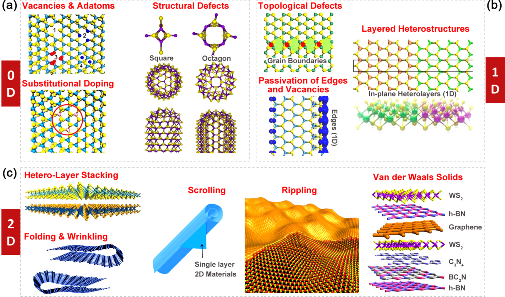
After introducing pristine crystal structures, we now proceed to classify structural defects. By definition, 2D TMDs could be infinitely large within their basal planes, but are only atomically thin perpendicular to the planes. Consequently, defects residing in these 2D crystals could be classified according to their dimensionality as zero-dimensional (point defects, dopants or 'non-hexagonal' rings; see figure 2(a)), one-dimensional (grain boundaries, edges, and in-plane heterojunctions; see figure 2(b)) and two-dimensional (layer stacking of different layers or vdW solids, wrinkling, folding, and scrolling; see figure 2(c)).

Figure 2. An overview of defects in 2D TMDs. (a) Typical zero-dimensional defects such as vacancies, adatoms, dopants, squares, and octagons. Reprinted with permission from [175]. Copyright 2000 American Physical Society. (b) Typical one-dimensional defects such as grain boundaries, edges, and phase interfaces. Reprinted with permission from [29]. Copyright 2014 Nature Publishing Group. (c) Typical two-dimensional defects such as folding, wrinkling, scrolling, rippling, and vertically stacked hetero-layers. Reprinted with permission from [111]. Copyright 2013 Nature Publishing Group. Reprinted with permission from [176]. Copyright 2012 American Chemical Society. Reprinted with permission from [177]. Copyright 2013 Wiley.
Download figure:
Standard image High-resolution image2.1. Zero-dimensional defects in TMDs
The simplest and most abundant defects in TMDs are vacancies, and the anti-sites that form on them (see figure 2(a)). In synthetic TMD samples, six varieties of intrinsic point defects are observed with regularity (see figure 3(a)): single sulfur vacancies (VS), double sulfur vacancies (VS2), a vacancy of a Mo atom and a triad of its bonded S within one plane (VMoS3), a vacancy of a Mo atom and all six of its nearest neighbors (VMoS6), an antisite, with Mo occupying a VS2 (MoS2), and a pair of S atoms occupying a Mo position (S2Mo) [24]. The notable absence of VMo from this list is likely due to its tendency to complex with sulfur vacancies. With the exception of MoS2, reconstruction of the structure is minimal upon forming vacancies, and the defects retain trigonal symmetries [24, 25]. VS has the lowest formation energy of these defects (∼2 eV) [24–27], but the exact value depends upon the chemical potentials μMo and μS. Given thermal equilibrium, μMoS2 = μMo + 2μS and both μMo and μS must be less than their values in bulk (an ambiguous figure for S, given its many allotropes) [25], the chemical potentials are constrained to certain values. It is a boon to experimentalists when defect formation energy calculations consider the full range of values for μMo and μS or at least the limiting sulfur rich and molybdenum rich conditions [25]. Without a full understanding of the thermodynamic parameters at play, it is a challenge to rationally produce defects on the lab bench.
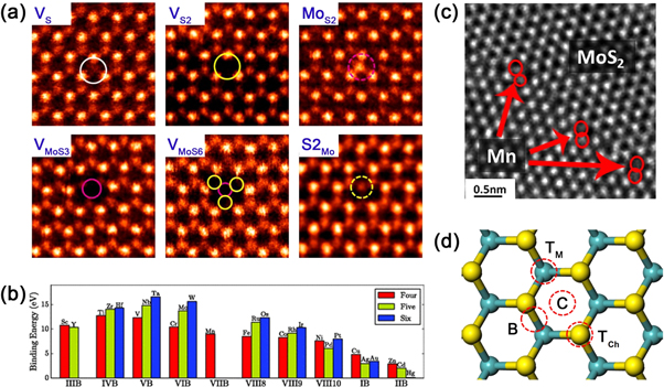
Figure 3. Zero-dimensional defects. (a) Atomic-resolution annular dark field (ADF) images showing different types of vacancy and vacancy complexes in MoS2 monolayers. Reprinted with permission from [24]. Copyright 2013 American Chemical Society. (b) Comparison of binding energies for MoS2 monolayers doped with transition metal atoms. Red, green and blue symbols correspond to dopants in group four, five and six, respectively. Reprinted with permission from [36]. Copyright 2013 American Physical Society. (c) TEM image showing MoS2 monolayers substitutionally doped by Mn atoms. Reprinted with permission from [41]. Copyright 2015 American Chemical Society. (d) A schematic diagram showing four sites of adatoms adsorbed onto TMD lattices.
Download figure:
Standard image High-resolution imageIt is also possible for other atomic species to replace lattice atoms by substituting elements. When considering the extent to which a foreign atom may substitute onto a crystal lattice, the ion's relative size, electronegativity, valence, and end member crystal structure are all relevant factors. The lanthanide contraction is a fortuitous periodic trend, which results in comparable radii for the 4d and 5d transition metals. This makes possible a wide variety of dopants from across the transition metal block. Notably, the similarity of W and Mo based on the criteria enumerated above allows for the formation of complete solid solutions in monolayer crystals [28]. In CVD grown TMD crystals, the extent of Mo/W alloying is heavily dependent on reaction kinetics, resulting in out- or in-plane heterostructures [29, 30], or a hybrid morphology [31]. S/Se alloying exhibits similar behavior [32–34]. While Mo/W and S/Se doping have been explored, there are few reports on the electronic and magnetic properties of other potential dopants (e.g. Mn, Co, Ni, etc).
To date, almost the entirety of the transition metal series has been examined with density functional theory (DFT) as substitutional dopants in MoS2 [35–40]. As can be seen by the calculated binding energies of transition metal dopants (see figure 3(b)) [36], with the exception of d9 and d10 elements, the possibility of substituting transition metal atoms onto the lattice appears quite favorable. Several metallic dopants other than W have already been observed experimentally in few to monolayer MoS2 films, including Mn (see figure 3(c)) [41], Nb [42, 43], Fe [44], Re [45], Au [45], and Co [46]. Similarly, substitution of many potential dopants onto chalcogen sites has been considered computationally [35, 39, 47]. While chalcogen site doping may be favorable in sulfur deficient crystals, excepting oxygen [48–51], to our knowledge no substitutive dopants have been identified experimentally. In addition to energy-dispersive x-ray spectroscopy (EDX) and x-ray photoelectron spectroscopy (XPS), two characterization techniques able to perform elemental and structural analysis of dopant atoms are the 'Z contrast' annular dark field microscopy (ADF) [52], a scanning transmission electron microscope (STEM) technique so called because of its sensitivity to differences in atomic number, and extended x-ray absorption fine structure, which can provide information such as coordination number and interatomic distances [43].
Rather than substituting onto the lattice, foreign atoms can be adsorbed to the crystal's surface. Such adatoms, are another form of defect that is of especial importance in 2D materials, due to their extreme aspect ratios. In the case of 1H phase TMDs, there are four positions available to an adsorbant (see figure 3(d)): above the metal atoms (TM), above the chalcogen atoms (TCh), on a metal–chalcogen bond (B), and above or within the center of hexagonal voids (C) [53]. In multilayer flakes, the TM and TCh sites are equivalent to intercalated species due to the 2H phase's stacking sequence [25]. In the case of electron donating alkali adatoms on MoS2, TM sites are predicted to be most energetically stable with adsorption energies approaching −1 eV in agreement with XPS data showing suppressed signal from the transition metal atoms [35, 54]. For many other potential adatoms [35, 53, 55], even more favorable adsorption energies have been predicted. Unsurprisingly, the most likely adatoms to be observed in MoS2 are Mo and S. While both adatom species have been observed on multiple sites via high angle ADF (HAADF) [24], it is predicted that S adatoms are stable only at TS, while Mo may rest either at TM or C [25]. Adatoms may be quite mobile under irradiation [45], and even at room temperature [35]. Thus, an understanding of adatom mobility may lead to insights into the kinetics and stability of TMD synthesis at elevated temperatures. Finally, we note that while not strictly zero-dimensional, some researchers have adsorbed molecular charge donors/acceptors to MoS2 flakes [56].
2.2. One-dimensional defects in TMDs
Extrinsic sulfur line vacancies result from the agglomeration of sulfur vacancies which are usually produced by electron bombardment [57]. Single- and double-line vacancies are observed experimentally, both aligned along the zig-zag direction (see figures 4(a) and (b)) [57]. This experimental result agrees with calculations which determine the formation energy of sulfur line vacancies in the zig-zag direction exhibit lower formation energies than those along the armchair direction [58]. In all cases, the formation energies of line vacancies are a function of the number of vacancies, in the range of 5–6 eV per vacancy for lengths of 6–16 [58]. When the freestanding edge regions are imaged by TEM, the orientation of line defects also depends on the strain. Thus, strain may serve as a means to select line vacancy orientations for tuning electronic properties [57].
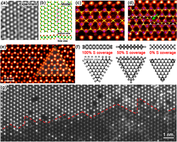
Figure 4. One-dimensional defects. (a) High-resolution transmission electron microscopy (HRTEM) image and (b) structural model showing a single vacancy line in MoS2 monolayers. Reprinted with permission from [57]. Copyright 2013 American Physical Society. (c) and (d) ADF images of 4|4P and 4|4E 60° grain boundaries in CVD MoS2 monolayers. Structural models are overlaid on ADF images. Reprinted with permission from [24]. Copyright 2013 American Chemical Society. (e) ADF image showing an inversion domain in monolayer MoSe2. Reprinted with permission from [61]. Copyright 2015 American Chemical Society. (f) Structural models showing Mo-terminated MoS2 domains edges with different percentages of sulfur coverage. Reprinted with permission from [63]. Copyright 2002 Elsevier Science (USA). (g) ADF image showing a 1D interface between monolayer MoS2 and WS2. Reprinted with permission from [29]. Copyright 2014 Nature Publishing Group.
Download figure:
Standard image High-resolution imageIn addition to sulfur line vacancies, grain boundaries are often observed in TMD monolayers. In comparison to one-atom-thick materials, TMD grain boundaries and the dislocation cores they are comprised of are quite complex. This is because three atomic layers compose TMD monolayers (i.e. chalcogen–metal–chalcogen). As atoms are removed, the structure relaxes in three dimensions, to form dreidel shaped dislocations with a variety of ringed motifs that are dependent on the grain boundary angle [59]. Patterns of two point-sharing four member rings (4|4P) form mirror twin grain boundaries in synthetic MoS2 and MoSe2 [24, 60], when grains meet at 60° angles along the zig-zag direction (see figures 4(c) and (d)). 4|4E metallic edge-sharing line defects are another possible 60° grain boundary morphology, which can result in triangular inversion domains with metallic edges (see figure 4(e)) [61]. The situation becomes more complex for smaller angles, with 4|6, 4|8, 5|7, and 6|8 motifs appearing. HAADF-STEM shows that on these low angle, and high strain (up to 58%) grain boundaries, sulfur atoms are quite mobile, even under low accelerating voltages, resulting in dislocation movement [62].
We now turn our attention to the most prominent defects in TMD flakes, their edges. Synthetic TMD single-crystalline islands most often adopt triangular shapes with edges that appear sharp in microscopic images. The triangular morphology of these flakes can be explained through the 2D application of the Wulff construction, which simply states that low energy edges will be preferred. These surface energies are a function of the μS, or the sulfur vapor potential. When μS is low (i.e., under low sulfur vapor pressures), MoS2 will adopt distorted hexagonal shapes rather than triangles. Nanoscale calculations predict that under the sulfur rich conditions prevalent during TMD growth, ( Mo edges with either 50% or 100% S (see figure 4(f)) are the most thermodynamically stable [63]. Nevertheless, in CVD grown samples the Mo-terminated edges with both 0% and 50% S coverage have been observed, suggesting that CVD is a process away from equilibrium [24].
Lateral hetero-interfaces constitute another form of 1D defect. Lateral (inner/outer) heterostructures of MoS2/WS2, MoSe2/WSe2, MoS2/MoSe2, and WS2/WSe2 have been reported recently [29, 30, 34]. Structurally coherent sharp interfaces (see figure 4(g)) have been observed as a result of covalent epitaxy between two dissimilar TMD layers with similar lattice constants.
2.3. Two-dimensional defects in TMDs
Perfect 2D materials have been predicted by theories as unstable upon thermal fluctuation, but after the discovery of graphene, it has gradually become clear that suspended graphene could stablize by the formation of ripples, i.e., finite surface roughness and deformation [64]. Similarly, ripples with a typical height on the order of nm have been observed in as-synthesized MoS2 monolayers (see figure 2(c)) [65, 66], and can be generated deliberately by scanning a laser beam over MoS2 monolayers [67]. Ripples introduce strain into the materials, and could well affect their electronic properties [65, 68].
In few-layered TMDs, adjacent layers are coupled by vdW forces. The magnitude of vdW forces depends sensitively on the interlayer spacing, which is correlated to stacking configuration. Most synthetic few-layered TMDs exhibit a Bernal stacking (AbA BaB...), but derivations from this stacking configuration are also possible, especially when TMD layers are stacked manually via transfer techniques [69]. Due to the handling of TMDs, it is also possible for flakes to fold over onto themselves [70]. For those that assume the 1H phase, folding produces a structure distinct from the 2H phase. As we will discuss in section 4, the vdW interface has strong impact on the electronic and optical properties of few-layered TMDs, therefore the interface associated with a stacking and layer orientation can be viewed as a 2D defect (see figure 2(c)).
There is a large family of known 2D materials, such as graphene, hBN, TMDs, and layered oxides. Given the similarity in their interlayer 'bonding', 2D materials of different kinds can be placed one on top of another, forming vertical heterostructures or vdW solids (see figure 5(a)) [71]. When the top layer (e.g. MoS2) has a crystal structural similar to the bottom layer (e.g. graphene) (see figure 5(b)), their stacking occurs via vdW epitaxy [72]. Compared to covalent epitaxy where adjacent layers are covalently bonded, vdW epitaxy is more tolerant to lattice mismatch between layers, thereby allowing a variety of 2D materials to be stacked in this way. The interfaces between vertical hetero-layers can also be viewed as 2D defects which generate new properties in the materials (see figure 2(c)). For example, when there is lattice mismatch, such as the cases of MoS2/MoSe2 and WSe2/graphene, vdW epitaxy results in periodic Moiré patterns (see figure 5(c)) [73, 74], and each pattern results in different optoelectronic properties that need to be studied in more detail.
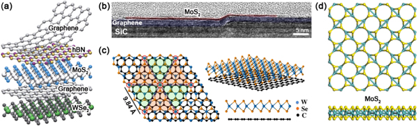
Figure 5. Two-dimensional defects. (a) Schematic representation of vdW heterostructures made by stacking different 2D materials. Reprinted with permission from [71]. Copyright 2013 Nature Publishing Group. (b) Cross-sectional transmission electron microscopy (TEM) image showing a 2D interface between MoS2 and graphene layers. Reprinted with permission from [72]. Copyright 2014 American Chemical Society. (c) Structural model showing a Moiré pattern in vertically stacked monolayer WSe2 and graphene. Reprinted with permission from [74]. Copyright 2015 American Chemical Society. (d) Relaxed structural models showing 8–4 MoS2 Haeckelites. Reprinted with permission from [75]. Copyright 2014 Institute of Physics.
Download figure:
Standard image High-resolution imageIn closing our classification of defects, we draw attention to the possibility of TMD Haeckelites [75]. In defective graphene and carbon nanotubes, Haeckelites are extended areas of 5|7 ring defects [76, 77]. In analogy, the geometry of TMDs allows for the formation of 6|8 Haekelites (see figure 5(d)). The structure and electronic properties of TMD Haeckelites have been predicted for a wide number of TMD materials: the semiconducting TMDs of Mo and W become semi-metallic, while metallic NbS2 and NbSe2 become small gap semiconductors [75]. Therefore, achieving defect control in these 2D systems is very important in order to tailor their electronic, optical and even magnetic properties.
3. Generation of defects in TMDs
The following subsections describe possible ways to generate defects in 2D TMDs. For example, the introduction of structural defects such as atomic vacancies and grain boundaries could be achieved under fluctuating growth conditions using chemical vapor transport (CVT) or CVD. Those defects are often unintentionally generated. However, the structural defects can be more deliberately generated post-synthesis by several approaches, such as ion/electron irradiation, plasma treatments and high-temperature annealing in the presence of different gases. These methods have started to be studied but should continue to be developed in order to achieve defect type and concentration control in TMD materials.
3.1. In situ generation of defects in TMDs
Among all synthesis methods to grow stoichiometric and crystalline TMDs, CVT has been the most adopted one to grow bulk large TMD crystals. In general, CVT involves transport of vaporized TMD powders in a sealed ampoule with a temperature gradient along its length. Each CVT synthesis typically takes several days to assure high-quality crystal growth at temperatures around 1000 °C [78]. As-grown crystals usually exhibit high degree of crystallinity, are usually free of contamination from the transport agents (e.g. Br2, or I2), and have been used extensively for exfoliation and based proof-of-concept research. For example, field effect transistors (FETs) made from exfoliated TMD flakes exhibit n-type (e.g. MoS2) or p-type (e.g. WSe2) behavior [11, 12], indicating that the channel materials are not defect-free. In fact, chalcogen vacancies and inversion domains have been observed in synthesized CVT crystals [79]. Each exfoliated flake naturally has edges, where the atomic structure and the chemical properties differ from the internal regions [80]. Besides single phase TMDs, CVT is also powerful in synthesizing doped (or alloyed) TMD bulk crystals [81]. Owing to the high growth temperature and long growth time, CVT grown crystals often possess structures with high spatial homogeneity. For example, CVT synthesized MoxW1−xS2 crystals show uniform distribution of Mo and W atoms in the entire crystal (see figure 6(e)) [28, 82], contrasting with CVD-synthesized MoxW1−xS2 alloys with an in-plane compositional gradient (see figures 6(b)–(d)) and CVD MoS2/WS2 heterostructures with a well-defined phase boundary (see figure 6(a)) [29, 31]. Similarly, CVT MoSxSe2−x alloys have randomly distributed S and Se atoms, whereas CVD MoSxSe2−x monolayers can be homogeneous alloys [32, 33, 83], non-uniform alloys [84], or phase-segregated heterostructures [34]. If we consider substitutional dopants as points defects, CVT typically guarantees a uniform distribution of point defects (see figure 6(e)), and more importantly, the density of point defects could be fine-tuned by adjusting the initial loading of reactants. A variety of dopants have been added via CVT, for several purposes, such as band gap engineering (MoxW1−xSySe2−y) [28, 85, 86], and charge doping (p-type Nb doping [43], and n-type Re doping [45]), but additional work in this area is needed. Other metal and chalcogen dopants need now to be introduced in monolayers and bulk crystals of TMDs.
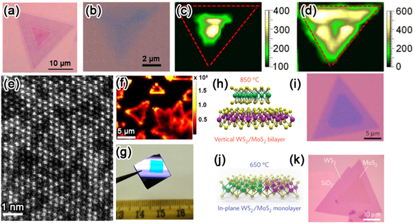
Figure 6. In situ generation of defects. (a) Optical image showing a 1D interface in a CVD grown monolayer MoS2/WS2 lateral heterostructure. Reprinted with permission from [29]. Copyright 2014 Nature Publishing Group. (b) Optical image showing an alloyed MoxW1−xS2 triangular domain with non-uniform optical contrast. Raman maps over this triangle are shown in (c) for the MoS2-E' mode intensity and (d) the WS2-E' mode intensity. Reprinted with permission from [31]. Copyright 2014 American Institute of Physics. (e) ADF image of homogenous Mo0.5W0.5S2 alloyed monolayer. Reprinted with permission from [82]. Copyright 2013 Nature Publishing Group. (f) PL map of isolated WS2 monolayer domains grown by CVD at atmospheric pressure. Reprinted with permission from [88]. Copyright 2013 American Chemical Society. (g) Digital photo showing a quasi-continuous large area WS2 film grown by CVD at a low pressure. Reprinted with permission from [92]. Copyright 2013 American Chemical Society. (h) Schematic and (i) optical image of vertical MoS2/WS2 heterostructure with a 2D interface grown by CVD at 850 °C. (j) Schematic and (k) optical image of in-plane MoS2/WS2 heterostructure with 1D interface grown by CVD at 650 °C. Reprinted with permission from [29]. Copyright 2014 Nature Publishing Group.
Download figure:
Standard image High-resolution imageBesides top-down synthesis methods such as the aforementioned CVT-mechanical exfoliation, bottom-up approaches have also found wide applications given their scalability. CVD is a typical bottom-up approach which involves chemical reduction of transition metal precursors by gaseous chalcogen precursors. When compared to CVT, CVD synthesis takes place on shorter time scales, at lower temperatures, and with more volatile precursors [87]. Owing to the relative violence of the technique, a large variety of defects can be generated and engineered in CVD-grown TMDs. For example, by adjusting the flow of sulfur vapor, it is possible to control the orientation and optical properties of domain edges, and the overall density of sulfur vacancies [88–90]. By varying the base pressure inside CVD reaction chambers, one can synthesize either isolated WS2 triangular domains (see figure 6(f)) or quasi-continuous WS2 films (see figure 6(g)) [88, 91, 92]. In principle, it is also possible to control the average grain size together with density of grain boundaries. By tuning growth temperatures during synthesis of MoS2/WS2 heterostructures, one can selectively generate either 2D interfaces (see figures 6(h) and (i)) or 1D interfaces (see figures 6(j) and (k)) [29]. Different from CVT, a two-step growth is feasible via CVD. The second step provides additional degrees of freedom to modify the properties of the starting materials (materials obtained in the first step). Two-step growth is particularly powerful when the first and second step require sufficiently different growth conditions or precursors. Examples of two-step growths include partial sulfurization of CVD diselenides [93], partial selenization of CVD disulfides [93, 94], and formation of lateral junctions by in situ switching precursors [30, 34]. Another distinct feature of CVD is that the properties of resulting materials depend largely on the choice of substrates [95]. The flatness, lattice constants, thermal stability and cleanness of substrates affect the density of grain boundaries, angle of grain boundaries, shape of domain edges, and domain orientations.
Bulk CVT- and CVD-synthesized disulfides and diselenides belong to the 2H phase (or 1H for monolayer). Chemically exfoliated disulfides sheets consist of 2H and 1T' phases [22]. The 1T' phase differs from the 2H phase in atomic structure and the electronic properties [22]. Here we would view the 1T' phase as an independent structural polytype rather than a defective derivative from the 2H phase (see figure 1). Therefore, the fascinating properties of the 1T' TMDs are unfortunately outside the scope of this article. Readers interested in this topic are encouraged to read a recent review by Voiry et al [22].
3.2. Ex situ generation of defects in TMDs
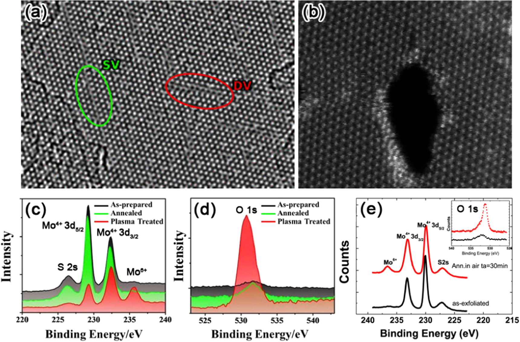
Besides in situ generation of defects during materials synthesis, recent progress also highlights the possibility of post-synthesis defect engineering. Previously, electron beam irradiation has been used to generate defects in graphene and hexagonal boron nitride (hBN) [5, 96]. Now this idea is extended to few-layered TMDs. First-principles calculations suggest that the threshold energy to generate chalcogen vacancies lies on the order of tens to hundreds of keV, which is accessible in state-of-the-art electron microscopes [47]. Indeed, sulfur vacancies are generated when TMD layers are subjected to energetic electron beams. The sulfur vacancies are mobile upon irradiation, migrating and agglomerating into vacancy lines (see figure 7(a)) or nanoscale holes if transition metal atoms are also removed (see figure 7(b)) [57, 97]. Interestingly, the electron beam damage can be reduced by sandwiching TMD layers between graphene layers, possibly because the highly electric and thermal conductive graphene layers reduce the charge and heat accumulations [97].

Figure 7. Ex situ generation of defects. (a) HRTEM image showing electron beam irradiation induced formation of single line vacancy (SV) and double line vacancy (DV) in monolayer MoS2. Reprinted with permission from [57]. Copyright 2013 American Physical Society. (b) HAADF image showing beam radiation induced formation of nanoscale holes in monolayer MoS2. Reprinted with permission from [97]. Copyright 2013 American Chemical Society. (c) and (d) XPS spectra of as-prepared, thermally annealed, and O-plasma treated MoS2. O-plasma treatment introduces O–Mo bonds. Reprinted with permission from [51]. Copyright 2014 American Chemical Society. (e) XPS spectra of as-exfoliated and thermally annealed MoS2. Annealing introduces O–Mo bonds. Reprinted with permission from [101]. Copyright 2014 American Institute of Physics.
Download figure:
Standard image High-resolution imagePlasma treatment has also proven effective to generate a variety of defects in TMD layers. Oxygen plasma treatment introduces O–Mo bonds (see figures 7(c) and (d)) [49–51], while argon plasma can be used to create sulfur vacancies [98], and to even remove entire TMD layers [99]. Moreover, SF6, CF4, and CHF3 plasma treatments can ripple and separate TMD layers [100]. In the future, it is possible that these techniques could be developed further in such a way that they could control the chemical functionalization and layer number in TMD or vdW systems. Further calculations on the effects of different functional groups or molecules on these systems should also be carried out.
Thermal annealing has also been employed to create sulfur vacancies and form Mo–O bonds in TMDs (see figure 7(e)) [13, 51, 101]. Alternative physical approaches for ex situ defects engineering include α particle bombardment [13], Mn+ ion bombardment [14], proton beam irradiation [102], ozone (O3) treatment [103], and laser illumination [80, 104], but detailed characterization studies on these defective systems are still needed.
4. Properties and applications of defective TMDs
In the following subsections, we demonstrate how different defects can alter the properties of TMDs. In certain cases, defects can widen the potential applications of TMDs. In other cases, defects provide a limiting factor for reliability and homogeneity in otherwise pristine materials.
4.1. Electronic properties of defective TMDs
As a semiconducting analogy to semi-metallic graphene and insulating hBN, MoS2 has great potential in electronics and optoelectronics [11]. The device performance of atomically thin MoS2 FETs depends on a variety of factors, including the material's quality, thickness, substrate, contacts, environment, and surface functionalization. Here we focus primarily on the effects of intrinsic structural defects on the transport characteristics. Zero-dimensional structural defects, such as sulfur vacancies (see figure 3(a)), are the most common defects in exfoliated and CVD MoS2 monolayers [24]. Sulfur vacancies introduce unpaired electrons into the lattice, n-doping the material [105]. PL measurements and first-principles calculations reveal that sulfur vacancies lead to the formation of a non-zero density of states within the band gap [13, 24, 106]. Localized electronic states are created around sulfur vacancies, and when the carrier density is low, electrons transport via hopping between localized defect states [106]. In addition to sulfur-deficient MoS2, sulfur-rich (or molybdenum-deficient) MoS2 has also been reported to show a p-type transfer behavior [105]. Both n- and p-type transports have been identified even from different regions of the same MoS2 sample (see figures 8(a) and (b)). Thus, it is evident that further efforts should be devoted to the control of local stoichiometry. Other point defects such as foreign atoms can also alter the electronic properties of TMDs. Doped TMDs such as MoxW1−xS2, MoxW1−xSe2 and MoSxSe2−x alloyed monolayers have been synthesized [28, 31–33, 82–86, 93, 94]. In these cases, doping induces an appreciable modulation in the band gap, as confirmed by PL measurements (see figure 8(c)). Notably, the band gap value does not change linearly with the stoichiometry, owing to the bowing effect [28]. Nb atoms can p-dope MoS2, which has been proposed theoretically and confirmed by transport measurements [35, 42, 43]. Re atoms are predicted by DFT to be n-type dopants [35], but experimental verification is lacking, and further measurements are needed.
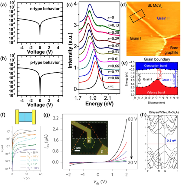
Figure 8. Electronic properties. (a) and (b) I–V curves from MoS2/Au contacts. (a) and (b) are measured from different regions of the same sample, showing opposite transfer behaviors. Reprinted with permission from [105]. Copyright 2014 American Chemical Society. (c) PL spectra of alloyed Mo1-xWxS2 monolayers with various compositions. Reprinted with permission from [28]. Copyright 2013 American Chemical Society. (d) STM image of monolayer MoS2 with a grain boundary separating two grains. (e) Band gap profile in the proximity of the grain boundary shown in (d), measured by STS. Reprinted with permission from [107]. Copyright 2015 Nature Publishing Group. (f) Top: schematic representation of a memristor based on MoS2 with a bisecting grain boundary. Bottom: I–V curves showing gate-tunable memristive behaviors. Reprinted with permission from [110]. Copyright 2015 Nature Publishing Group. (g) I–V characteristics showing a p–n diode behavior. The device is based on a lateral heterojunction composed of p-type WSe2 and n-type WS2 monolayers. An optical image of the device is shown as inset. Reprinted with permission from [34]. Copyright 2014 Nature Publishing Group. (h) DFT calculated band structure of WSe2/MoS2 hetero-bilayers with the A-type stacking configuration. The direct gap transition is indicated by a vertical arrow. Reprinted with permission from [111]. Copyright 2013 Nature Publishing Group.
Download figure:
Standard image High-resolution image1D defects such as vacancy lines, inversion domains, and grain boundaries also affect the electronic properties of TMD layers. Sulfur line vacancies can interconnect into a triangular loop, encompassing an inversion domain rotated 60° from its surroundings. The change of stoichiometry at the edge of the inversion domains introduces mid-gap states, which are contributed primarily by the Mo orbitals [79]. Similarly, in MoSe2 monolayers grown by molecular beam epitaxy, deviation from the stoichiometry in a Se-deficient condition leads to the formation of inversion domains defined by Se-deficit mirror twin boundaries. Theoretical calculations suggest that the conductance of the mirror twin boundaries is enhanced as a result of additional spatially localized states within the band gap [60]. Depending on the atomic structures, grain boundaries in MoS2 can be either sulfur-deficient or molybdenum-deficient, and therefore locally n-dope or p-dope the material [90]. Band gap variation in the proximity of grain boundaries have been detected by scanning tunneling microscope (STM)/ scanning tunneling spectroscopy (STS) (see figures 8(d) and (e)), suggesting local changes in the electronic structure [107]. Line defects can also reduce the rotational symmetry of the two-dimensional basal plane, and raise in-plain anisotropy in quantum conductance [108]. Grain boundaries in CVD grown MoS2 monolayers modulate the in-plane electrical conductivity [90], while grain boundaries in metal organic chemical vapor deposition (MOCVD) grown polycrystalline MoS2 monolayer films show less disturbance on the spatial homogeneity of transport characteristics [109]. Although considerable efforts have been devoted to eliminating grain boundaries and building devices on large single crystalline MoS2 domains, polycrystalline MoS2 has recently found new applications in gate-tunable memristors where grain boundaries play an essential role (see figure 8(f)) [110]. Hetero-interfaces between two stitched dissimilar TMD monolayers are another type of 1D defect that have begun to draw attention. Recent advances in synthesis allow lateral epitaxial growth of MoS2/WS2 and WS2/WSe2 in-plane heterostructures, where the 1D interfaces serve as p–n junctions (see figure 8(g)) [29, 34].
When TMD monolayers are stacked along the vertical direction, the top layer interacts with the bottom layer via vdW force. The vdW interface can be viewed as a 2D defect which brings in new properties. For example, single phased semiconducting TMDs such as MoS2 and WSe2 experience a direct to indirect gap transition when the layer number goes beyond just one. However, first-principles calculations predict that hetero-bilayers are not necessarily indirect band gap semiconductors [111]. It is possible that a stacked hetero-bilayer has a direct band gap in energy lower than that of each constituent layer (see figure 8(h)) [111]. The electronic properties of homo- and hetero-bilayers depend on the original properties of each constituent layer, on the stacking angle and inter-layer spacing [29, 73, 112–121]. Moreover, new functionalities such as vertical rectifying junctions, photodiodes, and resonant tunneling diodes have been achieved in stacked MoS2/WSe2 layers [122–124].
4.2. Optical properties of defective TMDs
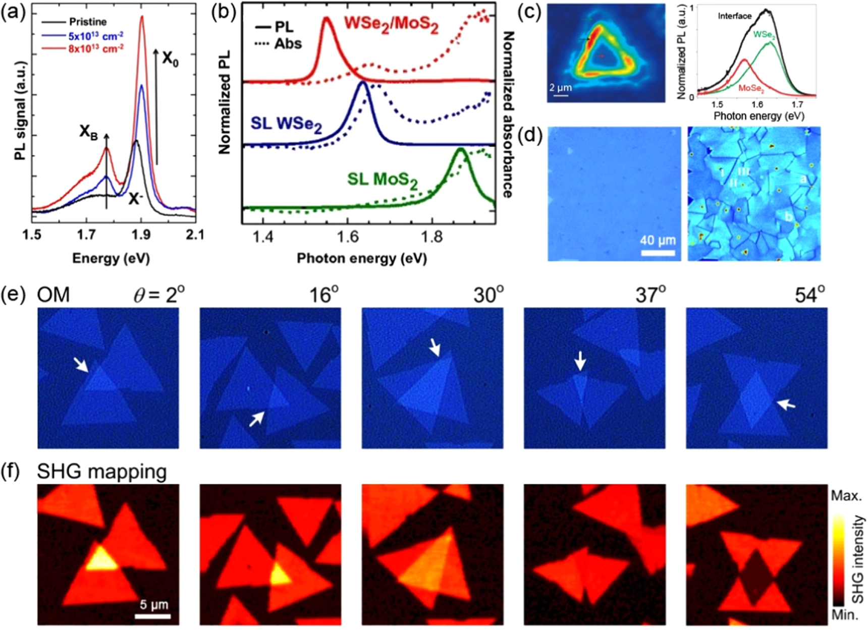
Optical properties of semiconducting TMD layers are strongly correlated to their electronic properties [7]. Defect induced changes in electronic band structure are often accompanied by appreciable changes in excitonic transitions [125]. An example given in section 4.1 shows that dopants induce band gap variation in semiconducting TMD monolayers, as well as a shift in the PL peak energy (see figure 8(c)). Beside the changes at band edges, subtle changes within the band gap can also introduce evident features in PL spectra. In exfoliated MoS2 monolayers with bi-sulfur vacancies generated by controlled plasma irradiation, a PL peak is observed with an energy below the band gap value (see figure 9(a)), attributable to neutral excitons bound to defects [13, 125]. Edges, common 1D defects in CVD grown TMD triangular single-crystalline domains, emit visible light with intensity similar or higher than that from the interior regions [88, 89]. The extraordinary edge PL emission can be understood by first principles calculations: with edge periodicity, transition metal valence states, and oxygen adsorption at edges taken into account, calculations show the edges of 2D TMDs can be semiconducting [126].
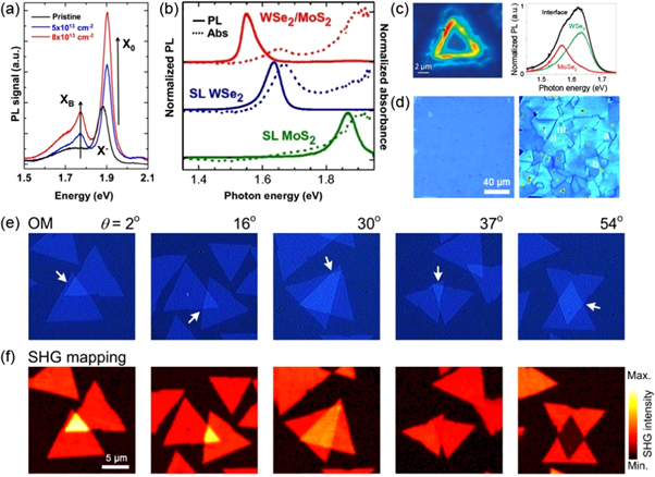
Figure 9. Optical properties. (a) Low temperature PL spectra at 77 K of pristine and α-particle irradiated MoS2 monolayers. Two irradiation doses used are 5 × 1013 cm−2 and 8 × 1013 cm−2. Neutral, charged, and bound excitons are labeled as X0, X−, and XB respectively. Reprinted with permission from [13]. Copyright 2013 Nature Publishing Group. (b) Normalized PL and absorbance spectra for monolayer MoS2, WSe2, and their hetero-bilayers. Reprinted with permission from [114]. Copyright 2014 the National Academy of Sciences of the United States of America. (c) Left panel: PL intensity map of a MoSe2/WSe2 lateral heterostructure. The colored arrows indicate regions of MoSe2, WSe2 and their interface. PL spectra taken from indicated regions are shown on the right panel. Reprinted with permission from [30]. Copyright 2014 Nature Publishing Group. (d) Left panel: Optical image of a polycrystalline MoS2 monolayer film. SHG image from the same area is shown in the right panel, where grain boundaries are visualized. Reprinted with permission from [131]. Copyright 2014 AAAS. (e) Optical images of artificially stacked MoS2 bilayers with various stacking angle (θ). Their corresponding SHG intensity maps are shown in (f). Reprinted with permission from [69]. Copyright 2014 American Chemical Society.
Download figure:
Standard image High-resolution imageAs discussed above, TMD layers are free of dangling bonds, and can be stacked vertically via vdW epitaxy. An atomically sharp 2D interface between adjacent layers can introduce novel optical properties that are absent in each layer when the stacked layers are sufficiently coupled. For example, as we have discussed in section 4.1, vdW stacking offers a possibility to tune the electronic band structure, and to enable new excitonic transitions in hetero-bilayers. This has been observed experimentally in mechanically stacked MoS2/WSe2 bilayers, that showed a strong PL emission at ∼1.50–1.56 eV, lower than the band gap energy of MoS2 (∼1.87 eV) and WSe2 (∼1.64 eV) (see figure 9(b)) [114]. Similarly, in CVD grown MoS2/WS2 hetero-bilayers, a PL peak at lower energy (∼1.4 eV) was observed [29]. Notably, this novel excitonic transition is spatially indirect, i.e. electrons and holes are from opposite layers due to type II band alignment in hetero-bilayers [114, 127].
TMDs could also share the same crystal structure and similar lattice constants, so they can be stitched together laterally without significant lattice misfit. MoS2/WS2 and MoSe2/WSe2 in-plane heterojunctions have been synthesized directly by vapor deposition methods [29, 30]. The transition from the first to the second phase occurs within an atomically sharp phase boundaries. The interface emits visible light with an energy lying between band gap values of the two phases, and with an intensity much stronger than those from both sides (see figure 9(c)) [29, 30].
Monolayer TMDs do not exhibit inversion symmetry, therefore certain nonlinear optical processes, such as second harmonic generation (SHG) are pronounced in monolayers [128–130]. The intensity of SHG signal depends on factors such as crystal orientation, excitation wavelength, and topological defects such as grain boundaries, and domain edges. In CVD grown polycrystalline MoS2 monolayer films, SHG is reduced in intensity along grain boundaries as a result of destructive interference of waves from neighboring grains [131]. These grain boundaries, though atomically thin and optically invisible, can be directly mapped out by second harmonic microscopy (see figure 9(d)). Molybdenum terminated zig-zag domain edges, on the contrary, enhance second harmonic response locally, as a result of changes in the electronic properties at 1D edges, where the translational symmetry of the 2D domains is broken [131]. Ideally, 2H (or Bernal) stacked TMDs with an even number of layers do not generate second harmonic signal [128–130]. However, if even-layered TMDs have a non-ideal stacking configuration, the SHG is not necessarily quenched. It has been shown using artificially stacked MoS2 bilayers that the SHG signal is recovered when the stacking order deviates from the intrinsic 2H stacking, owing to the lack of inversion symmetry [69]. Moreover, the intensity of SHG depends on the stacking angle which modulates the interference of second harmonic signal generated from each constituent TMD layer (see figures 9(e) and (f)). It is very likely that other nonlinear optical effects could be observed in different 2D systems, and research should concentrate on the synthesis of doped heterolayers.
4.3. Vibrational properties of defective TMDs
Raman spectroscopy is an ideal and non-destructive technique to study the vibrational properties of 2D TMDs, as it provides rich information about different physical and structural properties of the samples [23, 78, 132–137]. In particular, Raman spectroscopy has been extensively used to identify number of layers [136, 138, 139], and to study the effects of charge-doping [140], strain [141, 142], and disorder [14, 96]. Interpreting Raman spectra of 2D TMDs requires understanding of the crystal symmetry. Here we review briefly the symmetry of the 2D TMDs for the trigonal prismatic phases (i.e. 1H and 2H phases). The symmetries of TMDs are layer dependent. TMDs with an odd number of layers are non-centrosymmetric, whereas TMDs with an even number of layers are centrosymmetric [78]. The 1H phase has three Raman active phonon modes which are assigned to the irreducible representation of the D3h group as  E' and E''. The
  mode corresponds to the out-of-plane atomic displacement where the upper and lower layers of chalcogen atoms vibrate in-phase but in opposite directions. In the case of the E' and E'' modes, the atomic displacements are in the plane. The E' represents a mode in which the chalcogen atoms move in-phase and the metal atoms move in the opposite direction, whereas the E'' mode involves only the in-plane vibration of the chalcogen atoms, but in opposite directions. The E'' mode is forbidden in a common backscattering Raman experiment, in which the incident laser beam is perpendicular to the basal plane of TMD layers [136].
The bulk 2H TMDs have four first-order Raman active phonon modes represented by the irreducible representations of the D6h group and are assigned as A1g, E1g,  and
and  The first three modes have similar origins as the
  E'' and E' modes in the 1H polytype. Thus, the E1g mode is also not observable in a common backscattering Raman experiment. The mode
  originates from the vibration of adjacent rigid layers with respect to each other, and appears in the low-frequency range [136]. Note that above observable Raman modes originate from a first-order process and involve phonons only at the Γ point which is the center of the Brillouin zone (BZ) [136]. This constriction is a direct consequence of conservation of momentum. However, in the presence of structural defects which can serve as scattering centers to enable momentum conservation, phonon modes within the interior or at the edges of the BZ such as the longitudinal acoustic (LA) mode near and at the M and K points can be activated. Therefore by tracking the defect activated Raman modes, we can gather important information about structural defects [14, 96, 136, 143, 144].
Considering that many researchers in the 2D community are very familiar with Raman spectroscopy of graphene [143, 144], we first give an example of studying defective graphene by Raman scattering [96]. Figure 10(a) depicts a Raman spectrum of defective graphene, which displays three main Raman features, the D, G and 2D (or G') bands. Here D band play a key role in understanding defects. The G band corresponds to the E2g phonon in the center of BZ. The D band is a disorder-induced band. This band involves an in-plane transverse optical (iTO) phonon near the K or K' points in the BZ that become Raman active activated via defects in the graphene lattice. For example, structural defects in graphene can be ex situ generated by ion irradiation. By changing the ion dose, one can change the average distance between defects (LD), or equivalently the defect density. As shown in the figure 10(b), the defect density has an evident correlation with the Raman intensity ratio of the D band over the G band, i.e., I(D)/I(G).
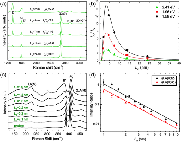
Figure 10. Vibrational properties. (a) Raman spectra of graphene with various defect densities, indicated by LD. The laser energy used to measure is 2.41 eV. (b) Raman intensity ratio I(D)/I(G) of graphene with various defect densities. Laser energies used for measurements are 2.41, 1.96 and 1.58 eV. Reprinted with permission from [96]. Copyright 2011 American Chemical Society. (c) Raman spectra of monolayer MoS2 with various defect densities, indicated by LD. (d) Raman intensity ratio I(LA)/I(E') and I(LA)/I of monolayer MoS2 with various defect densities. Laser energies used for measurements are 2.33 eV. Reprinted with permission from [14]. Copyright 2015 American Physical Society.
Download figure:
Standard image High-resolution imageSimilarly, defects in monolayer MoS2 can be created intentionally via Mn+ ion bombardment [14]. High dose of ion bombardment significantly enhances the relative intensity of the LA mode at M point (see figure 10(c)). The LA mode has a similar origin as the D-band in graphene since they both involve phonons near the edge of BZ and are activated by structural defects. Similar to defective graphene, in defective MoS2 monolayers, the Raman intensity ratio I(LA)/I or I(LA)/I(E') could serve as an indicator to quantify the defect density (see figure 10(d)). Similarly, defects in other semiconducting chalcogenides such as WSe2, WS2, MoSe2, etc are also expected to be characterized by analyzing the evolution of the LA mode as well as other resonant modes such as 2LA at the M point as the number of defects increase within mono- or few-layers. Progress along this direction is likely to be reported in due course.
The low-frequency range is relatively less explored for 2D materials, mainly due to the lower intensities of the low-frequency peaks compared to the E' and  modes, and because these peaks typically lie outside the range (<100 cm−1) of conventional Raman spectroscopy systems. The two most significant peaks in the low frequency region for layered 2D materials are the rigid shear mode, involving the relative motion of atoms in adjacent layers, and the layer-breathing (LB) mode, involving out-of-plane displacements of atoms in adjacent layers. Naturally these modes are absent in the Raman spectrum from monolayer TMDs and only appear for two layers and above. The shear mode, also called the C mode for coupling, was first shown to vary in frequency as a function of graphene layers [145]. Similar to the case of graphene, the C mode has been measured by different groups in mono- and few-layered MoS2, and WSe2 [146–149]. For example, it is located at 35 cm−1 for bulk MoS2 and decreases in frequency down to ∼20 cm−1 in bilayer MoS2. On the other hand, the LB mode, which is absent in bulk MoS2, increases in frequency. Since odd (even) layers lack (possess) inversion symmetry, the scaling of the C and LB modes are different with decreasing layer thickness [148, 149].
In addition to the C and LB modes, under resonant or near-resonant conditions (for example with a laser energy of 1.96 eV) a new peak has been observed at ∼40 cm−1 in monolayer MoS2 [147, 150]. Since this peak appears in the monolayer, it cannot be assigned to one of the rigid layer modes. Instead, the peak has been assigned to either electronic Raman scattering caused by the spin–orbit splitting of the conduction band [147], or to occurring from a strong resonance between excitons and polaritons [150]. Its origin is therefore unclear, and further theoretical and experimental works are required to fully understand the nature of this resonant peak.
Owing to the relative difficulty in obtaining spectral data in the low-frequency region, thus far low-frequency Raman spectroscopy has been the focus of just a few studies. With increasing opportunities for preparing heterostructures with different layered TMDs (vdW solids), the low-frequency modes are very useful for directly measuring interlayer coupling in 2D materials. Recent studies have shown the appearance of a new LB mode and suppression of the C mode in stacked MoS2/MoSe2 and MoS2/WSe2 heterostructures, whose frequency decreases with increasing stacking mismatch angle [151]. In addition, the relative intensities and frequencies of the C and LB modes have shown to vary (much more reliably than the high frequency modes) depending on stacking orientation (i.e. between the 2H and 3R configurations) in MoSe2/WSe2 heterostructures [152]. Raman spectroscopy in the low frequency range therefore offers the opportunity to investigate the effect of dopants, interface coupling, intercalants, and lattice mismatch in a wide variety of heterostructures or vdW solids composed of 2D TMDs.
4.4. Magnetic properties of defective TMDs
Compared to the electronic and optical properties, the magnetic properties of layered MoS2 and WS2 remain less exploited. Diamagnetism and ferromagnetism have been observed in different samples of MoS2 [153, 154], but the overall saturated magnetization in bulk MoS2 is not large enough to be utilized in applications such as spintronics. To render MoS2 truly magnetic, additional efforts have been made to tailor the material's microstructure. Irradiation has proven an effective method of enhancing ferromagnetism in bulk MoS2, presumably by generation of vacancies [153]. Scaling down the thickness of MoS2 serves as another way to induce magnetism. Experimentally, several types of magnetism, including diamagnetism, paramagnetism and ferromagnetism have been identified in different samples of mono- and few-layered MoS2 [155, 156]. Considering magnetic moments may be highly localized in samples, global magnetization measurements themselves may not provide enough spatial resolution to discover the origins of magnetic ordering. To this end, first-principles calculations have shed some light. Spin polarized calculations suggest that one-dimensional edges of two-dimensional MoS2 or WS2 carry non-zero net magnetic moments associated with unpaired electrons (see figure 11(a)) [155, 157]. The edge ferromagnetism agrees with the experimental observation that TMD nanosheets possess larger magnetizations than their bulk counterparts. Grain boundaries also induce two types of long-range magnetic orderings in the host nanosheets depending on the tilt angles of grain boundaries [158]. Low angle boundaries composed of stitched 5|7 dislocation cores exhibit ferromagnetic behavior while high-angle boundaries' 4|8 rings are antiferromagnetic (see figure 11(b)). Besides utilizing native synthetic defects in TMDS, an alternative strategy to introduce magnetic ordering is to dope the materials. Therefore, the full series of 3d transition metal atoms, including Sc, Ti, V, Cr, Mn, Fe, Co, Ni, Cu and, Zn have been considered as substitutional dopants within the framework of DFT [36, 38, 40, 159–162]. Mn, in particular, seems to be a promising candidate for the introduction of long-range ferromagnetic ordering into the host material [38, 40]. Significantly, calculations suggest Mn doped MoS2 monolayers can exhibit a Curie temperature above room temperature, which is appealing for application in diluted magnetic semiconductors. Recently, doping Mn atoms into MoS2 monolayers has been achieved by using a modified CVD process, in which dimanganese decacarbonyl (Mn2(CO)10) powders were added as Mn precursors, and graphene was used as a growth substrate [41]. Along this line, further experimental studies on Mn doping induced magnetism are expected.
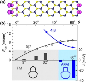
Figure 11. Magnetic properties. (a) A structural model of WS2 nano-ribbons with zig-zag edges. The calculated distribution of spin density is overlaid. Reprinted with permission from [157]. Copyright 2014 American Institute of Physics. (b) DFT calculated grain boundary magnetism in monolayer MoS2 as a function of tilt angle (θ). Considering the grain boundary energies (EGB), a small tilt angle (θ < 47°) favors 5|7 dislocations, whereas a high tilt angle (θ > 47°) favors 4|8 dislocations. Grain boundaries composed of 5|7 dislocations are ferromagnetic (FM), indicated by a positive exchange coupling parameter (J) in the 1D Ising model. Grain boundaries composed of 4|8 dislocations are antiferromagnetic (AFM), indicated by a negative J. Reprinted with permission from [158]. Copyright 2013 American Chemical Society.
Download figure:
Standard image High-resolution image4.5. Chemical properties of defective TMDs
Because pristine TMD basal planes are largely chemically inert, introducing a reasonable amount of defects is crucial in chemical applications. MoS2 can be extracted from mines and has long been considered as a low-cost catalyst for producing hydrogen, a clean alternative to fossil fuels, via hydrogen evolution reaction (HER) [163]. Bulk MoS2 shows a relatively low catalytic activity, while when thinned down to few or monolayers the performance is significantly improved. Owing to the rapid progress in the synthesis of atomically thin layers, MoS2 has been revisited in recent years as an effective catalyst [8, 20, 164]. The active sites for HER lie along one-dimensional edges of MoS2 nanosheets while the basal planes are catalytically inert, as confirmed by recent experiments and DFT calculations [163, 165]. Efforts have been therefore made towards creating or exposing more active edges. It has been demonstrated that by quickly sulfurizing molybdenum films deposited on a flat substrate, MoS2 sheets are formed with basal planes perpendicular to the growth substrate, thereby exposing a high density of one-dimensional edges (see figures 12(a) and (b)) [166]. The vertically standing MoS2 layers can also form on curved substrates such as nanotubes, in which case the density of exposed edges is further increased [167]. Another strategy to enhance catalytic performance is generating new edges via defect engineering [168]. The basal planes of MoS2 sheets can be cracked chemically to introduce additional defects with unsaturated bonds (see figures 12(c) and (d)) [169, 170]. Besides increasing edge density, incorporating foreign atoms, introducing the metallic 1T phase, and forming nanocomposites, have also proven feasible strategies to make MoS2 a more efficient catalyst [169, 171–174]. However, the possibilities are endless if we consider other TMDs different from MoS2 and their heterostructures.
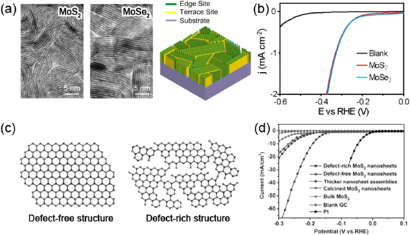
Figure 12. Chemical properties. (a) TEM image of vertically aligned MoS2 layers, MoSe2 layers, and a schematic presentation showing exposed edge sites. (b) Polarization curves of vertically aligned MoS2 layers, MoSe2 layers, and blank glassy carbons showing their HER performances. Reprinted with permission from [166]. Copyright 2013 American Chemical Society. (c) Schematic representations of defect-free and defect-rich MoS2 nanosheets. (d) Polarization curves of defect-free MoS2 nanosheets, defect-rich MoS2 nanosheets and several other materials as indicated. Reprinted with permission from [170]. Copyright 2013 Wiley.
Download figure:
Standard image High-resolution image5. Conclusions and perspective
In this review, we have categorized structural defects in 2D semiconducting TMDs based on their dimensionalities and atomic structure. We have summarized pathways to generating structural defects, including in situ generation during the materials synthesis, and ex situ generation after synthesis. Defects significantly alter the original electrical, optical, vibrational, magnetic, and chemical properties of materials. However, it is encouraging that the effects of structural imperfections in 2D TMDs are not necessarily detrimental. In certain cases, defects provide benefits to material properties, enhancing device performance, and enabling unprecedented functionalities.
Given the short history of research on 2D TMDs, the study of their structural defects is still in its infancy and most of the work summarized here corresponds to MoS2. In the years to come, three complementary directions may become attractive to researchers entering this field. The first is to avoid defects by synthesizing high-quality materials. For example, efforts will continue towards increasing the grain size of CVD TMDs and reducing the number of grain boundaries. This direction is particularly important for proof-of-concept studies, for setting a baseline of the so-called intrinsic properties, and for applications which require large-scale spatial homogeneity such as electronics. The second potential direction is the rational creation and utilization of defects. Towards this end, more work about basal plane chemical functionalization (see figure 13) is expected as well as studies of how defects affect mechanical and thermal properties of TMDs. At present, atomic scale understanding and manipulation of defects remains a challenge. For example, the dynamics of local defect formation, migration and reconstruction are largely unexplored. It is also challenging for experimentalists to introduce defects of specific types into desired locations and at controlled concentrations. The third potential direction is to heal defects, i.e. to convert defective TMDs into highly crystalline materials after synthesis. Given the high temperature and complicated dynamics during synthesis, it is impractical to fully avoid defects. Therefore, it may be necessary to develop approaches to eliminate certain synthetic defects after the fact. Recent advances in electron microscopy, optical spectroscopy, optoelectronics, and first-principles calculations have been bringing us new knowledge about defects on an almost daily basis. In light of this, it is not overly ambitious to expect breakthroughs in aforementioned directions to be on the horizon with joint efforts from physicists, chemists, materials scientists and engineers.

Figure 13. Surface functionalization. A scheme showing that S vacancies in MoS2 sheets can be passivated by thiol conjugation. Reprinted with permission from [178]. Copyright 2013 American Chemical Society.
Download figure:
Standard image High-resolution image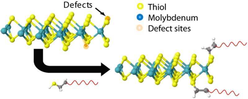
Acknowledgments
This work was supported by the US Army Research Office MURI grant W911NF-11-1-0362, the Air Force Office of Scientific Research MURI grant FA9550-12-1-0471, by the Materials Simulation Center of the Materials Research Institute, the Research Computing and Cyberinfrastructure unit of Information Technology Services and Penn State Center for Nanoscale Science. MT acknowledges support from the Penn State Center for Nanoscale Science (DMR-0820404 and DMR-1420620). The authors acknowledge the Center for 2-Dimensional and Layered Materials at the Pennsylvania State University. BRC and MAP acknowledge the financial support of Brazilian agencies FAPEMIG, CNPq and CAPES, and the Brazilian Institute of Science and Technology (INCT) in Carbon Nanomaterials. RL acknowledges the support from the National Natural Science Foundation of China (Grant No. 51372131, 51232005) and 973 program of China (No. 2014CB932401, 2015CB932500). HT and MT acknowledge the financial support from the National Science Foundation (2DARE-EFRI-1433311 & 2DARE-EFRI-1542707). RR acknowledges funding from the Air Force Office of Scientific Research.