

Abstract
One-dimensional (1D) and two-dimensional (2D) nanostructured zinc oxide (ZnO) thin films were electrodeposited from aqueous zinc chloride on FTO glass substrates. The effects of organic surfactant such as cetyltrimethyl ammonium bromide (CTAB) and polyvinyl alcohol (PVA) on structural, morphological, crystal quality and optical properties of electrodeposited ZnO films were investigated. The x-ray diffraction pattern revealed that the prepared thin films were pure wutrzite hexagonal structure. The thin films deposited using organic surfactant in this work showed different morphologies such as nanoplatelet and flower. The hexagonal platelet and flower-like nanostructures were obtained in the presence of CTAB and PVA surfactant, respectively. The crystal quality and atomic vacancies of the prepared nanostructured thin films were investigated by micro Raman spectroscopic technique. The emission properties and optical quality of the films were studied by photoluminescence spectrometry. PEMA-LiClO4-EC gel polymer electrolyte has been used to replace the liquid electrolyte for reducing the leakage problem. Graphene counter electrode was used as an alternative for platinum electrode. Eosin yellow dye was used as a sensitizer. J–V characterizations were carried out for different 1D and 2D nanostructures. The nanoflower structure exhibited higher efficiency (η = 0.073%) than the other two nanostructures.
Export citation and abstract BibTeX RIS
1. Introduction
Interest in the study of dye sensitized solar cell (DSSC) has developed for a few decades due to easy fabrication, low production cost and flexibility compared to conventional photovoltaic cells. Currently, the most successful high efficiency DSSCs consist of TiO2 nanoparticle as a photoanode and platinum as a counter electrode separated by (I−/I3−) liquid electrolyte [1]. Zinc oxide is one of the interesting materials with unique optical properties and high electron mobility compared to titanium oxides. It has high exciton binding energy (60 meV) and also n-type (II–IV) semiconductor with wide band gap of 3.37 eV at room temperature [2]. Besides that, single crystalline 1D ZnO nanostructure has shown good electron transport collection with fast electron transfer mobility in the order of 2–3 compared to TiO2 [3]. This can be used as Piezo-electric, light emitting diode, gas sensor, field emission, optical waveguides, dye sensitized solar cell [4] and thin film transistor [5]. According to Law et al [6] and Lupan et al [7], one can do direct electron transfer between the photoexcited dye and the back contact with reduced recombination losses in 1D nanostructure. In recent decades, the different ZnO nanostructures have been synthesized as a thin film by various growth methods such as physical vapour deposition [8–11], chemical vapour deposition [12, 13], sol–gel method [14], spray pyrolysis [15–17], conventional heating [18] and electrochemical deposition method [19]. Among these methods, electrochemical deposition method is low cost and it is easy to synthesize different nanostructures, such as nanowire, nanorod, nanopillar, nanoparticle, nanoplatelet and nanowall. Memarian et al have obtained high efficiency (η = 7.5%) for ZnO DSSCs in hierarchical aggregate structure by using N719 Dye [20]. The addition of the organic surfactant in the deposition solution has greatly changed and controlled the morphology and structural properties of the prepared thin film [19]. Inamdar et al have observed different nanostructures, such as granular shape and lamellar nanostructure with the addition of the organic surfactant in the deposition bath [21]. Zhang et al have prepared graphene based counter electrode to replace the Pt electrode. Graphene has attractive properties such as high electronic conductivity, corrosion resistance and low cost [22]. Rahman et al have used PVA-LiClO4 polymer electrolyte in photoelectrochemical cell to replace the liquid electrolyte, which has some disadvantages such as large weight, leakage and instability [23].
In the present work, we have prepared 1D and 2D ZnO nanostructured film without and with addition of organic surfactants as a photoanode into the zinc chloride precursor by electrochemical deposition method. In order to reduce electrolyte leakage problems in DSSCs, PEMA-LiClO4-EC based gel polymer electrolyte has been prepared by solvent casting technique, which we used as an electrolyte. Low cost graphene counter electrodes have been deposited by electrophoretic deposition to replace Pt electrodes. The morphology, structural and optical properties have been studied. J–V characterizations have been carried out for different 1D and 2D nanostructures using Keithley 4200-SCS source meter.
2. Experimental details
The electrodeposition experiments were carried out in a conventional three electrode cell. The deposition bath containing a mixture of 50 mM ZnCl2 (Merck, reagent grade) and 0.1 M KCl (SRL, reagent grade) as a supporting electrolyte were dissolved in deionized water. The pH of the aqueous solution was adjusted to 5.5 by adding diluted HCl. Molecular oxygen was continuously bubbled prior to deposition for 10 min and during the deposition process with constant stirring to diffuse oxygen molecule into the whole bath. The bath temperature was maintained at 80 °C. The Fluorine doped tin oxide (FTO) glass plate was used as a working electrode. The exposed area and resistance of the FTO glass is 0.50 cm2 and 15–20 ohm cm−2, respectively. Prior to electrodeposition, the substrates were ultrasonically cleaned for 5 min in acetone and ethanol each and further etched for 2 min in dilute nitric acid then finally washed with deionized water. Platinum and Ag/AgCl were used as counter and reference electrodes, respectively. A potentio/galvanostat electrochemical workstation (Princeton Applied Research Model 362) was used to deposit different nanostructured ZnO thin films potentiostatically at −1.2 V versus Ag/AgCl at a scan rate of 20 mV s−1. The distance between the working and counter electrode was 2 cm. All of the deposition time was fixed for 15 min. After deposition, the nanostructured ZnO thin film was thoroughly rinsed with deionized water and ethanol. To study the effect of organic surfactant on nanostructured ZnO thin film, various concentrations of cetyltrimethyl ammonium bromide (CTAB) and polyvinyl alcohol (PVA; MW = 115 000 g mol−1) were added separately in definite proportion to the aqueous precursor solution. The prepared samples were annealed at 350 °C for 1 h to remove the organic surfactants.
The morphologies of the prepared thin films were observed by JEOL, JSM-840 A scanning electron microscope instrument. The crystal structure was performed by a PAN Analytical X'Part PRO Powder x-ray diffraction meter. Room temperature photoluminescence of the thin films was carried out by Varian carry ellipse photoluminescence spectroscopy. The crystal phase and quality of the material were investigated from Micro Raman spectroscopy (Princeton instrument Acton SP 2500).
2.1. Counter electrode preparation
Graphene was prepared by a simple two-step process. First, graphene oxide was synthesized by Hummer's method and it was reduced by electrophoretic deposition in the form of graphene thin film [24]. The precursor aqueous solution contained a mixture of 8 mg graphene oxide (GO) and 5 mg cetyltrimethyl ammonium bromide (CTAB), which was used as a wetting agent. GO and CTAB were dispersed and dissolved in 15 ml deionized water. Then, 50 μl of hydrazine monohydrate was added as reducing agent into it. Graphene solution was ultrasonicated for 30 min prior to deposition. The solution was stirred continuously at 90 °C for 10 min. Pt and FTO glass plate were used as a counter and working electrode, respectively. The depositions were performed at 5 V for 30 min. Finally, the prepared thin films were thoroughly rinsed with deionized water and annealed at 350 °C to remove residue.
2.2. Electrolyte preparation
The poly ethyl methacrylate (PEMA) based gel polymer electrolyte was prepared by solution casting technique [25]. The electrolyte solution containing 25% of polymer PEMA, 8% of lithium perchlorate (LiClO4) salt and 67% of ethylene carbonate (EC) plasticizer was dissolved in tetrahydrofuran (THF) solvent. The dissolved polymer solution was stirred for 24 h to obtain a homogeneous mixture. Finally, the polymer solution was allowed to evaporate THF slowly until jelly state had been achieved. The obtained jelly solution was cast on Petri dishes to get the film. Then, the film was further dried at 60 °C for 12 h to remove the THF residue traces present in the film. The resulting film was shown to be free-standing in nature.
2.3. DSSC construction
The different nanostructured ZnO thin films were sensitized with 100 μM eosin yellowish dye in 10 ml ethanolic solutions for 12 h. After sensitization, the electrode was washed with ethanol to remove the excess dye present on the surface of the electrode. The cell was constructed by using eosin dye sensitized ZnO film as a photoanode, graphene electrode as counter electrode and then the two electrodes are sandwiched and separated by Li ion based polymer electrolyte. The current–voltage was measured using a Keithey 4200-SCS source meter using a 0.01 Vs−1 voltage sweep rate. The constructed solar cell was illuminated with 50 mW halogen lamp, whose J–V characterization was also studied and is interpreted in the results and discussion section.
3. Results and discussion
3.1. Surface morphology
Figure 1 shows morphology of the three different nanostructured ZnO thin films synthesized electrochemically on fluorine doped tin oxide glass substrate and the inset figures show a lower magnification (10000X) image of the nanostructures. The different morphology variations have been obtained by changing surfactants in the precursor aqueous solution. The nanowire array has been synthesized without an addition of surfactant in 50 mM concentration of ZnCl2 as shown in figure 1(a). The length and diameter of the synthesized nanowires have varied about 0.8–5 μm and 90–153 nm, respectively. The nanowires are grown one over the other parallel to the surface of the substrate, and these are not grown uniformly in the vicinity of the substrate. Lewis et al have synthesized similar nanowires on the seed layer coated FTO substrate in Zn(NO3)2 and hexamethylenetetramine (HMTA) electrolyte solution by hydrothermal method [26]. When 0.1 M (2% wt) cetyltrimethyl ammonium bromide was added into the deposition solution, the nanowires were converted into hexagonal plates and sheet-like structure as shown in figure 1(b). The observed hexagonal platelets are grown along the C-axis to the surface of the substrate, whereas nanosheet is grown parallel (axial direction) to the surface of the substrate. The attachments of two nanoplatelets and sheets have been noticed to form a single nanostructure. The nanosheet did not have any definite structure, whereas the platelet has a definite structure. The length and breadth of this platelet are about 1.8 μm and 0.2 μm, respectively. The surface of the hexagonal platelet and sheet are made up of the agglomerated particle; these will have given a high surface area to dye loading for a solar cell. The particle size of the platelet is varied about 42–70 nm. Qiu et al have synthesized nanoplatelet like structure on ITO substrate from nitrate solution bath without addition of any surfactant [27]. An on par innovation had also been reported by Pradhan et al [28]. When 0.1 M (0.1%) poly vinyl alcohol (PVA) is added in aqueous solution, flower-like nanostructures are obtained, as shown in figure 1(c). These flowers are made up of interconnecting hexagonal plates. All plates are amalgamated perpendicular to each other and look T-shaped. The length and thickness of these plates are about 2 μm and 90 nm, respectively. The hexagonal plate-like structure are made up of agglomerated particles, whose size has varied about 62–106 nm, and an interconnecting plate has also formed a different compartment-like structure, such as hexagonal, triangular or rectangular. Sharma et al have deposited thin film using PVA as an organic surfactant into acetate solution bath. The surface morphology of the film has been observed as a grain-like structure [29].

Figure 1. SEM images of thin films prepared with different organic surfactants (a) pure ZnO, (b) ZnO: CTAB (2%), (c) ZnO: PVA (0.1%) and (d) GO: CTAB (5 mg).
Download figure:
Standard image High-resolution imageFigure 1(d) shows SEM image of the graphene (counter electrode) thin film. A flower- like graphene nanorod array was observed, when cetyltrimethyl ammonium bromide surfactant was added into graphene oxide precursor at 90 °C. The flower-like nanorod array has not fully grown on the surface of the substrate. The breadth of the nanorods is varied about 76–92 nm.
3.2. X-ray diffraction
The XRD patterns of the prepared thin films are shown in figures 2(a)–(c). The prominent diffraction peaks are well indexed with those of the wutrzite hexagonal structure (JCPDS no.76-0704). The intensity of the prominent peaks depends on the morphology (see figures 2(a)–(c)) of the electrodeposited ZnO nanostructures.

Figure 2. XRD patterns of ZnO film deposited on FTO substrates using various organic surfactants into zinc chloride solution: (a) pure ZnO, (b) ZnO: CTAB (2%) and (c) ZnO: PVA (0.1%).
Download figure:
Standard image High-resolution imageFor nanowire, the planes at (002) and (101) are more intensive than the (100) plane. This indicates that the prepared nanowires are grown normal to the surface of the substrate and their preferred growth direction as in figure 2(a). The plane at (101) is intensive, it has inferred their preferential growth direction of nanosheet. The intensity of the (002) plane is more intense compared to reference pattern; it may be a growth of hexagonal nanoplatelet grown long the C- axis direction. For nanoflower-like structure, the prominent plane at (101) plane is due to their preferential growth direction. The unassigned weak peak appears at the left side of (100) plane. From this some level of disorder in the crystals is ascertained, perhaps driven by the complex folding of the nanoflower. Apart from the planes (100), (002) and (101) and the other diffracted planes (102), (110), (103), (200), (112) and (201) are indicative of random orientation of the nanostructures. From x-ray diffraction pattern, the rate of intensities of the diffraction plane of nanoplatelet structure is found to be high compared to the other two nanostructured ZnO films. From this it is revealed that the crystallinity of the nanoplatelet structure is high compared to nanowire and nanoflower structures. The crystalline sizes of the obtained nanostructures are estimated by using Scherrer formula [30].

Where K is the shape factor, λ is the wavelength of the incident radiation, β is the full width half maximum and θ is the diffraction angle. The crystalline size of the obtained nanowire, nanoplatelet and nanoflower are found to be about 30 nm, 40 nm and 27 nm, respectively.
3.3. Raman spectra
Raman spectra have been carried out for different nanostructured ZnO thin films annealed at 350 °C for 1 h, and this method is highly sensitive to identify the structural properties such as atomic vacancy, defect, size and shape of the nanoscale material. All of the spectra are shown in figures 3(a)–(d). In ZnO, the atoms have attached by ionic, covalent bonds and long-range coulomb field leading to the splitting of the A1 and E2 vibration. The B1 modes are inactive, whereas the E1 modes are active and ZnO has C6v point group [31]. The fundamental frequencies of the phonon optical mode in pure ZnO have E2(low) = 101 cm−1, E2(high) = 437 cm−1, A1(TO) = 380 cm−1, A1(LO) = 574 cm−1, E1(TO) = 407 cm−1 and E1(LO) = 583 cm−1 [32]. When the light is incident perpendicular to the ZnO surface, A1 (LO) and E2 mode are observed; the rest of the modes are forbidden according to Raman selection rule [33].

Figure 3. (a)–(d). Micro Raman spectra of different nanostructed ZnO and Graphene thin film with various scan rates.
Download figure:
Standard image High-resolution imageIn the present study, there are six bands appearing in the synthesized different nanostructured ZnO thin films E2H, E2L, A1 (TO), A1(LO) and E2L–E2H, respectively. The predominant E2H modes at 435 cm−1 are observed due to the heavy vibration of oxygen atoms in the nanowire, hexagonal platelet and flower-like structure, and also these modes belong to the hexagonal wutrzite structure and non-polar optical phonon mode of the ZnO, which is asymmetric due to the phonon confinement [31]. The increasing intensity of the flower-like structure indicates that the increasing crystal quality is compared to other two different structures. The frequency of the three nanostructured ZnO thin films is shifted 2 cm−1 to the lower number compared to bulk ZnO materials. It indicates that an increase in strain and defect existed in these materials [34]. The weak and broad peak centered at 324 cm−1 is attributed to second-order Raman scattering arising from zone boundary phonon E2H–E2L in ZnO [35]. The weak peak located at 384 cm−1 is due to the polar A1 transverse optical mode in nanowire [36]. The peak around at 156 cm−1 is due to the E2L (low) mode [32]. The E2L (low) mode is assigned to the vibration of heavy Zn sub lattice in ZnO [37]. The strong and broad A1 (LO) modes observed at 572 cm−1 are assigned to oxygen vacancies or disorder active Raman scattering in nanowire and nanoflower. These peaks were shifted 8 cm−1 from 572 cm−1 to 580 cm−1 due to the change of free carrier concentration in hexagonal platelet structure [32]. The peak centered at 1141 cm−1 is associated with second-order and multi-phonon process [38]. Although our XRD pattern shows sharp diffraction peaks for nanoplatelet, in Raman spectra a weak peak at E2H and strong broad peak A1(LO) are noticed. This is indicative of poor crystal quality of nanoplatelet and the presence of defect and vacancies in nanowire. From these close observations, one can know that nanoflower-like structure exhibited better crystal quality compared to other nanostructures.
Figure 3(d) shows a micro Raman spectrum of graphene at different scan rates such as 25, 30 and 35 s for nanoflower, rod-like structure deposited on FTO substrate. The increasing scan rate has increased the intensity of the spectrum. The intense G band peak from nanorod-like graphene layers in the sample is observed at 1578 cm−1, which is from two in-plane optical phonons related to the first-order Raman scattering or the in-plane stretching mode of sp2 carbon [39]. The predominant 2D band peak appearing at 2693 cm−1 is attributed to the two-phonon double resonance process and the highest optical branch phonon near the K point at the Brillouin Zone boundary in graphene [40]. The weak D band peak located at 1349 cm−1 is assigned due to the breathing mode of K-point phonon of A1g symmetry and the presence of disorder [39, 41]. The Raman intensity ratio from D band and G band (ID/IG) is used to estimate the graphene quality [42]. In our work, the intensity ratio of ID/IG is 0.88, which is less than 1, indicating flower-like nanorod has a few defects. The intensity ratio I2D/IG > 2, 1–2 and <1 have been matched to single-, double- and many-layer graphene [40]. Here, the I2D/IG ratios are 1.13, 1.17 and 1.21 for different scan rates 25, 30 and 35 s, which represents that the prepared graphene has bilayer.
3.4. Photoluminescence spectra
The room temperature photoluminescence spectra of electrodeposited nanostructured ZnO thin films are shown in figures 4(a)–(c). The prepared samples have shown six emission peaks, one for near band edge emission in the ultra violet region and another five peaks for deep level emission in the visible region [43]. The UV emission peak centered at 390 nm for nanowire and hexagonal platelet structures are related to the recombination free exciton and radioactive recombination of holes present in the valence band and electrons in the conduction band in ZnO thin films [44]. A small red shift from 390 to 392 nm in the flower-like structure occurs due to the interstitial zinc in the crystal lattice [43]. Xu et al have already reported that the UV emission peak might be shifted due to shape changes [45].
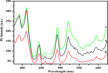
Figure 4. Photoluminescence spectra for different nanostructured ZnO thin films: (a) nanowire, (b) hexagonal platelet and nanosheet and (c) nanoflower.
Download figure:
Standard image High-resolution imageIn the violet region, the peaks centered at 410 and 435 nm are attributed to zinc and oxygen vacancies [46]. The blue emission peak at 492 nm can be assigned due to the impurities and native defects of interstitial zinc atom in the ZnO thin crystal [45]. Recently, Lee et al had explained that the blue emission is attributed due to the transition between donor and acceptor level related to interstitial hydrogen and oxygen atom [47]. The dominant peak centered at 521 nm is almost related to oxygen vacancy and this green emission is attributed to the recombination of photo-generated hole with singly ionized oxygen (O−) vacancies [46] and some researchers also reported that this emission is associated with intrinsic defect, zinc vacancy and interstitial oxygen or anti-site oxygen [48]. A yellow emission peak located at 595 nm is observed due to the presence of OH group and oxygen vacancy, oxygen interstitial defect [49]. The optical quality of the prepared nanostructured ZnO thin film can be studied from UV to VIS emission ratio [43]. The UV to Vis ratio of the nanowire, nanoplatelet and nanoflower are 0.9, 0.9 and 0.9, respectively. From these UV to Vis ratios, it can be concluded that all the prepared nanostructures are excited in the same optical quality.
3.5. J–V characterization
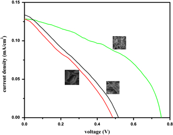
Figure 5 shows the current density and voltage (J–V) plots for different nanostructured ZnO films under illumination of 50 mW by halogen lamp. The open circuit voltage (Voc), short circuit current density (Jsc), fill factor (ff) and efficiency (η) are given in table 1. The efficiency of the DSSCs is highly dependent on the morphology and crystallinity of the nanostructures. The nanoflower-like structure exhibited higher (η = 0.073%) efficiency compared to other two structures. This is because nanoflower shows high crystal quality compared to nanowire and nanoplatelet structure observed in Raman spectra and small crystalline size estimated from XRD analysis, which offers a higher surface area for dye loading. In our study, all of the nanostructures showed lower efficiency, because all the samples have exhibited high defect as observe from PL spectra. In the present work we conclude that the reduction of efficiency is mainly due to high defects. In general, efficiency and fill factor of the solar cell depends on their internal resistances (shunt and series). The ideal solar cell has higher shunt and low series resistance. The shunt resistance is related to electron recombination between transparent conducting substrate/electrolyte and electron back transfer. The series resistance is related to resistance between the counter electrode/electrolyte interface, the resistance of the ion diffusion in the electrolyte and resistance of the conductive substrate. In the present work, nanoplatelet and nanowire show lower Voc and fill factor (ff) compared to nanoflower structure, which is related to shunt resistance due to electron recombination between electrolyte/FTO substrate and back transfer electron/excited dye molecule [50].
Figure 5. J–V curve of the ZnO nanostructures: (a) nanowire, (b) hexagonal platelet and nanosheet and (c) nanoflower.
Download figure:
Standard image High-resolution image
Table 1. Photovoltaic parameters of the DSSCs on the nanowire, nanoplatelet and nanoflower.
| S. No | Sample | Jsc (mA cm−2) | Voc (V) | Fill Factor (ff) | Efficiency (η) % |
|---|---|---|---|---|---|
| 1. | a | 0.135 | 0.517 | 0.37 | 0.051 |
| 2. | b | 0.131 | 0.486 | 0.22 | 0.028 |
| 3. | c | 0.129 | 0.751 | 0.38 | 0.073 |
4. Conclusion
Different nanostructured ZnO thin films were prepared on FTO glass plate by electrodeposition in the presence of organic surfactants such as CTAB and PVA in zinc chloride bath. The crystal structures were analyzed and their sizes were calculated. 1D and 2D morphology changes were observed by simply changing the organic surfactants. The hexagonal flower structures exhibited good crystallinity compared to the other two structures, which was concluded from the increasing intensity of the E2H band. The optical qualities of the prepared thin films were the same from UV to Vis ratio and also showed a high defect in the visible region. J–V characterization was performed for all the nanostructures. Nanoflower structure has exhibited high efficiency (η = 0. 073%). It has some advantages such as low cost, long-term stability and is leakage free. However, the performance of the device has to improve for practical application.
Acknowledgments
The authors would like to acknowledge the funding agencies UGC-BSR, New Delhi for providing financial support to be carried out this work.