

Abstract
The synthesis of cadmium sulfide CdS nanowires NWs by laser ablation of cadmium target in thiourea solution is demonstrated for the first time. The effect of laser fluence on the structural, morphological and optical properties of CdS nanoparticles was investigated. The synthesized CdS nanowires were polycrystalline with pure hexagonal wurtzite phase; as confirmed by x-ray powder diffraction results. The 3.18–3.26 eV direct optical energy gap of CdS and the increase of CdS optical absorption were noticed to be function of laser fluence. The results revealed a blue shift of 0.86 eV in the absorption edge of CdS nanowires when prepared at 2.65 J cm−2. The infrared absorption spectra revealed the presence of Cd-S stretching vibration peak located at (525–700) cm−1. Raman spectra confirmed the presence of a sharp peak at 304 cm−1 with intensity increased at higher values of laser fluence. Photoluminescence at room temperature indicated an emission peak of CdS at 471 nm. The scanning electron microscopy SEM investigation of the synthesized CdS showed a mixture of hexagonal nanoparticles and nanowires arrays. Transmission electron microscopy TEM investigation revealed the formation of well-dispersed single CdS nanowires with diameter in the range (18–27) and tens of micrometers long. The effect of laser fluence on the performance of n-CdS NWs/p-Si heterojunction was investigated.
Export citation and abstract BibTeX RIS
1. Introduction
Nanostructured semiconducting materials are used extensively in nano devices and photonics due to their excellent optical and electrical properties [1–3]. Due to its wide and direct band gap (2.4 eV at 300 K), optical absorption and stability, CdS found potential applications in semiconductor laser, nonlinear optical devices, solar cells, gas sensors, and biological applications [4–6]. Sol-gel, chemical vapor deposition (CVD), spry pyrolysis, dc-sputtering and pulsed laser ablation (PLA) are some methods used in CdS synthesis [1, 4, 5]. Depending on their chemical and physical properties, orientations and arrangements, the one-dimension nanowires and nanorods CdS serve as building blocks of many Nano devices, such as LEDs, Nano-generators and field effect transistors (FET) [7]. Recently, Ahmed et al [8] reported the preparation of pure hexagonal CdS nanoparticles by using laser ablation of CdS target in methanol. Their results indicated a varying band gap from 2.5 to 2.8 eV depending on laser fluence. Non-linear effect of nanoparticles had been reported when ablating different targets by laser in liquid; LAL. In this technique, nanoparticles (NPs) dispersion non-linearity was improved by silica microsphere focusing of the incident laser beam, and enhanced more by combining the strengths of liquid and solid phases, with non-linear tunability achieved by varying NPs concentration. [9–11]. Using (532 nm) Nd: YAG laser ablation in water, carbon NPs; with a strong optical limiting response, and spherical low coercivity cobalt NPs were obtained [12, 13]. In the present study, colloidal CdS nanowires were synthesized for the first time by pulsed laser ablation of cadmium target in Thiourea solution. The effect of laser fluence on the CdS NWs characteristics and CdS NWs/Si heterojunction photodetectors was demonstrated and discussed.
2. Experiment
Q switched Nd: YAG laser operating at 1064 nm wavelength and 9 ns pulse duration was employed, together with 12 cm positive lens, to prepare CdS colloidal solution by ablating high purity (99.9%) Cd pellet in Thiourea solution. All chemicals used in this experiment were reagent grade without any further purification The ablation solution was prepared by mixing 10 mM Thiourea (CH4N2S); as a sulfur source, with 50% ethanol (used here to prevent CdO formation), and 3.57 mM cetyltri-methyl-ammonium bromide CTAB [(C16H33)N(CH3)3]Br as a surfactant. The laser ablation was materialized at (26.54–39.82 J cm−2) laser fluences using 200 laser pulses on Cd pellet in an opened glass vessel; containing 4 ml of the ablation solution at a level of 0.5 cm above the Cd target. Converging lens with focal length of 10 cm was used for focusing the laser beam. The laser spot diameter on the Cd target located at 1 mm after focal point was 250 μm; measured with the assistance of an optical microscope. The optical absorption of the colloidal CdS nanowires solution was measured by using UV–Vis double beam spectrophotometer (Shimadzu, 00912901-S.Korea). The structure and crystalinity of the produced nanoparticles were investigated by using x-ray diffractometer (XRD-6000, Shimadzu). Scanning electron microscope SEM (T-scan Vega III Czech) equipped with energy dispersive x-ray was also employed to study the structure and chemical composition of the CdS nanowires. The Raman spectroscopy of the CdS nanowires was investigated using Bruker Raman microscope. The transmission FT-IR spectra of CdS nanowires were measured using Shimadzu 8000 spectrometer. The photoluminescence spectra of the CdS nanowires were recorded by Shimadzu RF-1501 spectrophotometer; which employs 345 nm line as the exciting wavelength. The shape and size of the CdS nanocrystals were investigated using transmission electron microscope type (CM10 pw6020, Philips, Germany). The conductivity type of the nanostructured CdS was estimated by Hall measurement. To fabricate CdS/Si photodetectors, drop casting technique was used to deposit thin layer of nanostructured CdS on p-type single crystalline mirror-like silicon substrate having electrical resistivity of 1–3 Ω cm. Ohmic contacts were established on both CdS layer and silicon substrate by depositing thin film of In-Ga and Al, respectively. Room temperature dark and illuminated current –voltage characteristics of the heterojunction were measured.
3. Results and discussion
The formation of nanostructured CdS can be explained as follows: focusing an intense laser beam on cadmium will rapidly heat its surface to a high temperature at the focal region. At very high laser fluence, a part of the vaporized cadmium is ionized (Cd2+) to form plasma, which absorbs the rest of the laser beam (see figure 1). As the metal vapor is heated more in the presence of the intense laser beam the absorption coefficient increases. At relatively lower level of laser intensities (26.54–39.82) J cm−2; the present experiment, partially ionized plasma is formed; meaning only part of the incident laser energy is absorbed. If the incident laser energy is above the breakdown threshold of cadmium, an intense evaporation will take place followed by the formation of thin plasma layer at the cadmium surface. Plasma formation is influenced by laser pulse duration, wavelength and energy. The CdS formation route is explained in the following equations [14]:
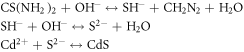

Figure 1. Photograph of laser –target interaction with plasma formation at laser intensity of 5.7 × 10⁹ W cm−2.
Download figure:
Standard image High-resolution imageThiourea interacts with the hydroxyl ion (OH−) to form (SH−). The latter interacts with (OH−) to form Sulfur ion (S2−) which interacts with cadmium (Cd2+) to form CdS nanostructure.
Colloidal CdS nanoparticles; prepared at various laser fluences after 24 h of ablation process, are presented in figure 2(a). At higher laser fluence the solution color changed from light to dark yellow; indicating higher value of colloidal particles concentration. The dark yellow CdS colloidal nanoparticles; freshly prepared at 39.8 J cm−2 laser fluence—figure 2(b) (i), has turned into brighter yellow after 10 min, due to some agglomeration, as depicted in figure 2(b) (ii).

Figure 2. (a) CdS colloidal nanoparticles prepared at various laser fluences after 24 h of ablation process, (b) CdS colloidal Nanoparticles (i) freshly prepared, and (ii) after 10 min of laser ablation with 39.82 J cm−2.
Download figure:
Standard image High-resolution imageFigure 3(a) shows the mass concentration of CdS nanowires as a function of laser fluence. As laser fluence rose from 26.54 to 39.82 J cm−2, the concentration of nanowires increased from 21 to 125 μg ml−1 due to increasing the ablated volume.

Figure 3. Mass concentration (a) and ablation efficiency (b) of CdS nanowires versus laser fluence.
Download figure:
Standard image High-resolution imageThe ablated mass m is related to the laser energy by the following relationship [15]:

Where R is surface reflectance, Eth is the ablation threshold laser energy, Cs is specific heat of the ablated target, ΔT is the temperature difference, λf is the latent heat of fusion, λc is the latent heat of evaporation. Figure 3(b) shows variation of ablation efficiency with laser fluence. At higher laser fluence than 35.39 J cm−2, ablation efficiency starts to saturate [16]. Figure 4 illustrates the effect of laser fluence on the absorption spectra of colloidal CdS nanoparticles. It shows the presence of a broad absorption peak at (450–490 nm) which agrees well with results obtained by another study [17]. Optical absorption enhanced at higher values of laser fluence due to the concentration rise of the ablated CdS particles.
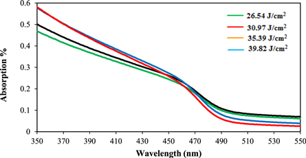
Figure 4. Optical absorption spectra of CdS nanowires as function of laser fluence.
Download figure:
Standard image High-resolution imageThe optical energy gap of CdS nanoparticles was estimated using Tauc's relationship;  Where; α is the absorption coefficient, A is constant and hυ is the photon energy. The resulted optical energy gap of CdS nanoparticles from the plot of (ahv)2 versus hv was direct transition type. The intersection of the straight line with hv axis gives the band gap value; as seen in figure 5. The energy gap values were found to be 3.21, 3.14, 3.08, and 3.06 eV corresponding to laser fluences of 26.54, 30.97, 35.39, and 39.82 J cm−2, respectively. The energy gap decreased when increasing laser fluence; due to the increased particle size [18]. The quantum size effect has led to 0.66–0.81 eV blue shift in the energy gap as compared to bulk CdS [8]. Figure 6 displays the laser fluence effect on FT-IR transmission spectra of the CdS NPs in the (400–4000)cm−1 range.

Figure 5. Variation of (αhv)2 versus photon energy plot for CdS nanowires.
Download figure:
Standard image High-resolution image
Figure 6. FT-IR spectra of CdS nanoparticles prepared at different laser fluences (a) 26.54 (b) 30.97 (c) 35.39 (d) 39.82 J cm−2.
Download figure:
Standard image High-resolution imageAll FT-IR spectra showed almost the same chemical bonds. The very strong absorption broad band at (3150–3500) cm−1 is indexed to O–H stretching vibration of water molecules. Trace of SO4− ions; as impurity, is seen as a small absorption peak at 1089 cm−1. Strong absorption band at (525–700) cm−1 is assigned to Cd-S stretching vibration [19]. The strong absorption peak at 1635 cm−1 represents the bending vibration of water molecules [20], and the C–O stretching is observed at 1044 cm−1 [21]. The weak peak at 2125 cm−1 indicates the presence of C≡C stretching band. No significant intensity variation or full width at half maximum (FWHM) absorption peaks of CdS NPs was noticed with increasing the laser fluence.
The XRD patterns of CdS nanowires; prepared at different laser fluences are shown in figure 7. The grown nanowires prepared at 26.54 J cm−2 are polycrystalline having diffraction peaks at 2θ = 24.9°, 25.6°, 26.4, 28.3, 43.8 and 47.5°, corresponding to (100), (002), (101), (102), (110), and (103) planes, respectively. These diffraction peaks are indexed to CdS hexagonal wurtzite phase according to JCPDS # 00-041-1049 [22, 23]. XRD patterns point out the disappearance of some diffraction peaks when increasing the laser fluence. The CdS nanoparticles diffracted intensity at (002) and (102) increased and became sharper, while the peak (110) almost remained unchanged at 30.97 J cm−2 laser fluence. At even higher values of laser fluence, the CdS nanoparticles grew only along the (110) plane (preferred orientation).

Figure 7. XRD patterns of CdS nanoparticles colloidal prepared at different laser fluences (a) 26.54 (b) 30.97 (c) 35.39 (d) 39.82 J cm−2.
Download figure:
Standard image High-resolution imageNeither cubic CdS phase diffraction peaks nor other elements, were detected; indicating the formation of high purity hexagonal CdS. The lattice constants of CdS nanowires were calculated and found to be a = 0.41 nm, c = 0.67 nm and c/a = 1.64. These findings are close to those reported in literatures [24]. EDS spectra of CdS nanowires; synthesized at various laser fluences, are given in figure 8. It shows the presence of Cd and S elements, in addition to some other peaks related to O, Mg, Na and Si elements; originated from the glass substrate. The high peak at zero represents some noise arose from the devise. Table 1 presents the effect of laser fluence on [Cd]/[S] ratio. CdS nanoparticles prepared at 26.54 J cm−2 laser fluence has [Cd]/[S] ratio of 1.2 (stoichiometry percentage of 80%); indicating small off-stoichiometric CdS nanowires. The large value of [Cd]/[S] ratio suggests the existence of sulfur vacancies and cadmium excess. At high laser fluence, sulfur could reach a temperature higher than its vaporization point; leading to higher [Cd]/[S] ratio.
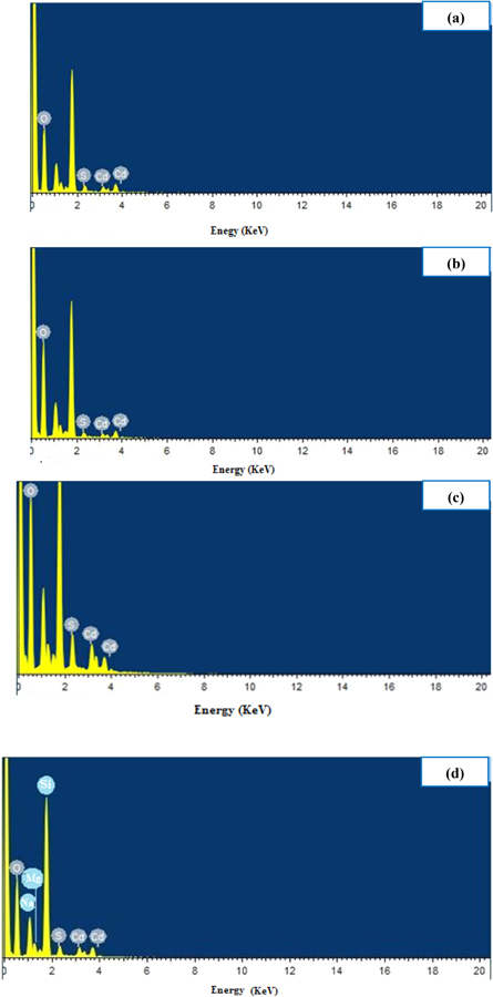
Figure 8. EDS spectra of CdS nanowires prepared at different laser fluences (a) 26.54 (b) 30.97 (c) 35.39 (d) 39.82 J cm−2.
Download figure:
Standard image High-resolution imageTable 1. Chemical composition (wt%) of CdS nanowires determined by EDS.
| Laser fluence | ||||
|---|---|---|---|---|
| Elements | 26.54 J cm−2 | 30.97 J cm−2 | 35.39 J cm−2 | 39.82 J cm−2 |
| S | 3.3 | 1.90 | 4.23 | 3.16 |
| Cd | 4 | 4.82 | 10.45 | 8.91 |
Figure 9 shows Raman spectra of CdS nanowires prepared at various laser fluences. These spectra illustrate strong fundamental peak located at 304 cm−1 and a weak overtone peak situated at around 600 cm−1. These peaks are related to longitudinal optical (1LO and 2LO) phonons; originated from phonon vibration [25, 26]. No shift in Raman peaks after increasing the laser fluence was noticed for both 1LO and 2LO peaks. The CdS nanowires; prepared at 26.54 J cm−2, exhibit the highest Raman intensity due to the nano-sized dimensions (quantum confinement effect). Besides; this figure reveals decreasing the FWHM and intensity of Raman peak with increasing laser fluence. Raman intensity of the CdS nanowires; synthesized with 39.82 J cm−2 laser fluence decreased six folds compared to its value when prepared with 26.54 J cm−2. This result could be ascribed to increasing the particle size and to particles agglomeration and aggregation effects. Slightly shift in Raman peak with increasing the laser fluence was noticed. Confinement of optical phonon resulted in an asymmetrical line shape and shift towards the low frequency region [27]. The values of vibrations obtained here are in good agreement with those of hexagonal wurtzite CdS nanoparticles prepared by using cyclic microwave radiation [28].

Figure 9. Raman spectra of CdS colloidal prepared at different laser fluences.
Download figure:
Standard image High-resolution imageThe SEM images of CdS nanoparticles demonstrated in figure 10 indicate a dependence of morphology and wires dimensions on laser fluence. Figure 10(a) illustrates a mixture of spherical nanoparticles and nanowires bundles observed when CdS was synthesized with (26.54 J cm−2) laser fluence. This figure shows an average nanowires diameter of 88.6 nm of several micrometers long. It also confirms the existence of well-dispersed and agglomerated nanowires. Agglomeration effect has led to the formation of micro-sized particles as shown in the inset of figure 10(a). At 30.97 J cm−2 laser fluence, the hexagonal nanoparticles started to formulate as shown in the inset of figure 10(b). Further increase in laser fluence has raised the concentration of nanoparticles and nanowires; as presented in figures 10(c) and (d). The present results indicate that wires grown at higher laser fluences have short lengths; meaning smaller CdS aspect ratio compared to those prepared at lower laser fluences. Particles and wires aggregation and agglomeration increased at higher laser fluence.

Figure 10. SEM images of CdS colloidal prepared at different laser energies: (a) 26.54 (b) 30.97 (c) 35.39 (d) 39.82 J cm−2.
Download figure:
Standard image High-resolution imageThe SEM images describe some CdS particles grown on the wires. An interesting morphology is given in figure 11 which reveals coaxial core–shell structure for CdS particles prepared at 39.82 J cm−2 laser fluence. Figure 12 elucidates some TEM images with CdS nanowires prepared at different laser fluences. These images reveal the presence of nanoparticles and nanowires of sizes and density which are laser fluence dependent.
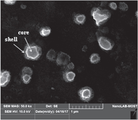
Figure 11. SEM image of core–shell CdS nanoparticles.
Download figure:
Standard image High-resolution image
Figure 12. TEM images and histograms of size distribution for CdS nanowires and nanoparticles prepared at different laser fluences (a) 26.54 (b) 30.97 (c) 35.39 (d) 39.82 J cm−2.
Download figure:
Standard image High-resolution imageAt low laser fluence, the produced nanowires are well-dispersed and single nanowires and could easily be seen by TEM (see figure 13). The nanowires are intersected with each other at different angles. The diameter of synthesized CdS nanowires increased at higher laser fluence. They were in the range of (18–27 nm) and few micrometers long. TEM observation also revealed that the synthesised CdS nanowires were smooth. Increasing the laser fluence to 30.97 J cm−2 has led to formation of some agglomerated nanoparticles on the nanowires (denoted by arrows); see figure 12(b). Figure 12(d) displays the formation of slightly dispersed nanoparticles with average size of 18 nm and arranged in certain pattern. This particle size is comparable to that determined by the broadening of XRD peak using Scherer's equation (21 nm). The particle size distribution of CdS nanoparticles; prepared at 3.98 J cm−2 is given in figure 14.
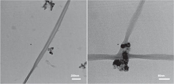
Figure 13. Different magnification TEM images of well-dispersed CdS single nanowires prepared at 26.54 J cm−2.
Download figure:
Standard image High-resolution image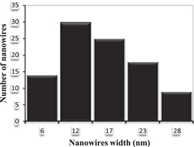
Figure 14. Particle size distribution of CdS nanoparticles synthesized at 39.82 J cm−2.
Download figure:
Standard image High-resolution imageFigure 15 shows the PL spectra of CdS nanowires prepared at different laser fluences. The PL spectra illustrate broad peaks; located at around 471 nm (green emission) corresponding to 2.63 eV which are not in agreement with optical absorption data. This could be due to presence of trapping states within the band gap of CdS [29]. Their emissions were red shifted compared to those of band edge emission. No significant shift in PL emission was observed after increasing the laser fluence. The PL intensity was found to increase with laser fluence. At 26.54 J cm−2, the PL intensity of CdS nanowires was approximately two times higher than that of CdS prepared at 39.82 J cm−2. In addition, the FWHM of PL emission increased from 71 to 83 nm as laser fluence was raised from 26.45 to 39.82 J cm−2. The broadening of PL peaks at high laser fluence is probably due to the existence of radiative and non-radiative recombination arising from traps, particles agglomeration, wide size distribution, and structural defects.

Figure 15. PL spectra of CdS nanowires prepared at various laser fluences.
Download figure:
Standard image High-resolution imageFigure 16 shows the dark current-voltage (I–V) characteristics of n-CdS NWs/p-Si heterojunctions at room temperature, which were prepared by various laser fluences at bias voltage ranged from −5 to +5 V. The inset of figure 16 is the cross-sectional view of n-CdS NWs/p-Si heterojunction. All heterojunctions exhibit laser fluence dependent rectifying properties. One thousand rectification factor at 5 V was obtained for heterojunction prepared at approximately 30.97 J cm−2. The heterojunction characteristics degraded at higher laser fluence; with rectification factor decreased to 362 at 5 V after increasing the laser fluence from 30.97 to 39.82 J cm−2. The forward current increases exponentially with bias voltage, and the reverse current was voltage independent. Figure 16 illustrates that the turn-on voltage increased with laser fluence due to the increased the laser resistivity of deposited CdS NWs layer. The ideality factor (β) of the heterojunction was calculated using the following equation:

Where If and Io are the forward and saturation currents respectively; estimated from a semi-logarithmic relationship of forward current against bias voltage plot. Table 2 lists the values of Io and β of the heterojunctions synthesized at different laser fluences. The β value is varying from 3.1 to 13; large value of β indicates poor diode characteristics. Structural defects, trapping and surface recombination processes represent the main contributors of increasing the value of β [30, 31]. The effect of laser fluence on illuminated I-V characteristics of heterojunction photodetectors is given in figure 17. The current was increased after illumination with white light due to the generation of e-h pairs. The on/off ratios (photocurrent to dark current ratio) at 5 V were listed in table 1. The ratio decreases from 12 000 to 4400 after increasing laser fluence from 30.97 to 39.82 J cm−2. This could be attributed to the decreased optical energy gap, particles agglomeration, surface morphology and surface to volume ratio. The values of on/off ratio are bit higher than of those reported for CdS NWs/Si prepared by other methods [32, 33].
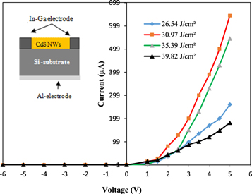
Figure 16. Dark I-V characteristics of heterojunctions. Inset is the architecture of n-CdS NWs/p-Si heterojunction and electrode configuration.
Download figure:
Standard image High-resolution imageTable 2. Values of saturation current, ideality factor and on/off ratio of heterojunction as function of laser fluence.
| Laser fluence (J cm−2) | Is (μA cm−2) | On/off ratio × 103 | β |
|---|---|---|---|
| 26.54 | 0.8 | 11 | 6.3 |
| 30.97 | 0.3 | 12 | 3.1 |
| 35.39 | 1 | 5.5 | 9 |
| 39.82 | 3 | 4.4 | 13 |

Figure 17. Illuminated I–V characteristics of heterojunctions with different laser fluences a) 26.54 (b) 30.97 (c) 35.39 (d) 39.82 J cm−2.
Download figure:
Standard image High-resolution image
Figure 17 also shows at higher light intensity there is an improvement in the photodetectors' photocurrent. This indicates photodetectors with fair linear characteristics.
4. Conclusions
Cadmium sulfide nanowires and nanoparticles of hexagonal phase have been successfully prepared by a new route using pulsed laser ablation of cadmium target in Thiourea solution. The laser fluence used in laser ablation process determined the size, length, shape, concentration and crystalinity degree of nanostructured CdS. The new route is very simple and can control the specifications of nanowires and nanoparticles through the laser fluence. The present findings are in context of the published work; emphasizing the effectiveness of the new route. The optical data revealed a blue shift of 0.81 eV in the absorption edge of CdS nanowires prepared at 26.54 J cm−2. Raman spectra illustrate strong fundamental peaks suited at 304 cm−1 and a weak overtone peak located at around 600 cm−1 which are belonged to longitudinal optical (1LO and 2LO) phonons. EDX results indicated a pure synthesized CdS nanostructure with best stoichiometry CdS percentage of ∼80%. The TEM observation demonstrated possible obtainment of well-dispersed single CdS nanowires in this route after selecting the appropriate laser fluence. The n-CdS NWs/p-Si heterojunction prepared at 30.97 J cm−2 gave the best characteristics.