
Abstract
Pure and Sb doped ZnO thin films were homogeneously prepared at room temperature on the soda-lime glass substrates (SLG) via the spin coating technique. The effects of the Sb ratio on structural properties, morphological properties and optical properties were studied via x-ray diffraction (XRD) device, scanning electron microscopy (SEM), and ultraviolet-visible (UV-vis) spectrometry, respectively. Crystalline size (D), the (hkl) planes, and dislocation density (δ) for ZnO thin films were investigated via the XRD pattern. The influence of Sb doping on the preferred crystal orientation and lattice parameters of ZnO thin films were discussed in detail. Optical measurements of ZnO thin films with 0, 1, 2 and 3% Sb concentrations showed a significant effect as a function of Sb dopants on the optical energy band gap. All of the SEM images indicated that while pure ZnO thin films had an apparent nanofiber structure, nanofiber structures disappeared with the increase of doping ratio, and more homogeneous films were obtained.
Export citation and abstract BibTeX RIS

Original content from this work may be used under the terms of the Creative Commons Attribution 4.0 licence. Any further distribution of this work must maintain attribution to the author(s) and the title of the work, journal citation and DOI.
1. Introduction
Recently, a binary semiconductor material of Zinc oxide (ZnO) and doped ZnO films, with a wide energy band gap value, highly transparent and large exciton binding energy, have been widely studied owing to nontoxic, abundant and their excellent properties such as electrical, optical and magnetic properties [1–4]. ZnO has been widely known as a promising material in various applications owing to the increasing need for short-wavelength devices [1, 2]. Indeed, it has found various applications, including piezoelectric, bio-sensors, transducers, varistors, window layers in solar cells, phosphors, transparent conducting films, UV resistive coatings and gas sensors.
ZnO films characteristically show n-type conduction at Zn rich conditions. It was occurred by a deviation from stoichiometry owing to 'intrinsic' donors such as oxygen vacancies, zinc interstitials and H incorporation [3]. On the other hand, the p-type conduction in ZnO is commonly defined by comparatively low hole mobility, instability and low hole concentration due to the deep acceptor levels of the dopants. Therefore, it is challenging to obtain p-type ZnO material owing to the likelihood of holes getting replaced by the native defects [4, 5]. In previous studies, N-In co-doped p-type ZnO [6], N-Al co-doped p-type ZnO [7], Cu doped p-type ZnO [8] and some homojunctions [9–11] have been presented. p-type ZnO was obtained by using group V elements such as N [12], P [13], Sb [14], and As [15] at Zn and O rich conditions. In recent years, based upon first-principle investigations, it was proposed that group V dopant Sb could indicate relatively shallow acceptor levels in ZnO, supposing that an Sb atom could replace a Zn atom and simultaneously cause two Zn vacancies in a process that contains fivefold as coordination [16]. Xiu et al reported that hall effect measurements indicated p-type conduction for ZnO films using a molecular beam epitaxy base on this theory [17]. Mandalapu et al demonstrated the first Sb doped p-ZnO/n-Si device performance. They suggested that Sb is a promising element for p-type doping in ZnO thin films for UV optoelectronic applications using molecular beam epitaxy [14].
To investigate ZnO films, several physical and chemical deposition techniques including magnetron sputtering [18], pulsed laser deposition [19], excimer laser deposition [20], sol-gel method [21], low-pressure metal-organic chemical vapor deposition (MOCVD) [22], ultrasonic spray pyrolysis technique [23] and sol-gel spin coating technique [24] have been used. The spin coating technique is an essential method for the prime necessity for obtaining good quality film because the advantage of this method includes the capability of controlling surface morphology, rate ratio, and geometric properties of the system.
In the present work, pure and Sb doped ZnO films were prepared using the spin coating method to contribute to the physical behavior of pure and Sb doped ZnO films in literature. For this purpose, the experimental results of all the films like structural, morphological and optical properties are comparatively examined.
2. Experimental
In the present study, to obtain 0.1 M of the pure ZnO solution at room temperature, 1.316 g of zinc acetate dihydrate (Zn (CH3COO)2 2H2O) was mixed with 60 ml of methanol. Sb doping solution was prepared by dissolving 0.0456 g of SbCl3 with 20 ml of methanol. To obtain the formation of clear, homogenous, and transparent solutions, solutions were stirred at room temperature for two h at room temperature. After the stirring process, this obtained solution was mixed with the pure ZnO solution to get a different atomic rate doping such as 0, 1, 2 and 3%. Before the fabrication process, soda-lime glass (SLG) as a substrate source was carefully cleaned to obtain dependable measurements. For cleaning, SLG substrates were firstly boiled in a mixture of different ratios of H2O, NH3, and H2O2 (5:1:1) for 20 min at 90 °C, then, the same ratio of H2O, H2O2, and HCl for 20 min at 90 °C. The cleaned substrates were firstly cleaned in deionized water and then ultrasonicated stirred in acetone and ethanol for 3 min, respectively. Before each fabrication process, the substrates were rinsed in deionized water for 3 min and then dried under N2 gas for 2 min. The films were then deposited on SLG substrates by spin coating method rotating at a spin rate of 2000 rpm for 75 s. All the thin films were heated for 10 min on a hot plate at 220 °C. This process repeated ten times. After the deposition, all the films annealed at 450 °C for one h in air ambient. X-ray diffraction patterns were taken by a Rigaku Ultima III diffractometer λ = 0.154 Å, at 40 kV, 30 mA. XRD data were collected in theta-two theta mode. Collected data were analyzed based on powder diffraction files provided by the International Center for Diffraction Data. The surface morphology of the layers was carried out using a Zeiss Evo 50 system scanning electron microscope (SEM). The absorbance value, which is used for the energy band gap for films, was measured using a Perkin Elmer Lambda 25 spectrophotometer.
3. Result and discussion
The surface morphology of all the films is investigated by SEM images that are a very significant instrument to research the microstructure of thin films. Figure 1 demonstrates that SEM images of both pure and Sb doped ZnO thin films for different Sb concentrations via spin coating technique. All of the SEM images show that the surface morphology was strongly effected depending on Sb doped increase. It can see from the figure that nanofiber structure formed in pure and 1% Sb doped ZnO. Komaraiah et al also observed similar structures using SEM images of spray pyrolysis technique for ZnO thin films [25]. When the Sb concentration attained 2 and 3%, it is clear to see the nanofiber structure disappears with the increase of doping ratio, which may be attributed to the influence of structural change resulting from replacing Zn2+ atoms with Sb3+ atoms. The SEM images show that the results of SEM are associated with the XRD results.
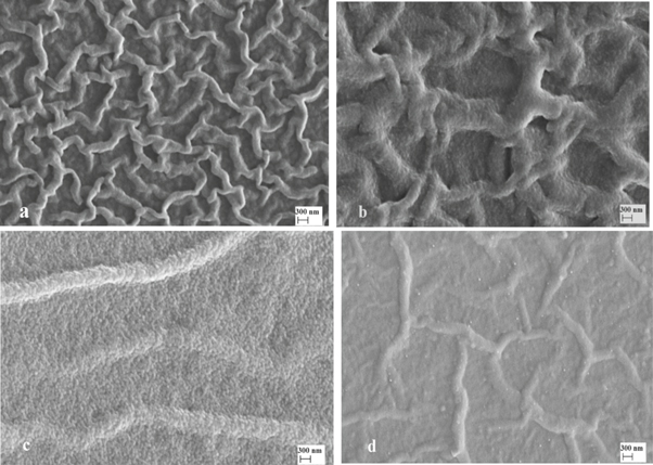
Figure 1. SEM images of (a) pure ZnO (b) 1% (c) 2% and (d) 3% Sb doped ZnO thin films.
Download figure:
Standard image High-resolution imageXRD patterns of pure and Sb doped ZnO thin films are presented in figure 2. As seen from the figure 2, (002) is the dominant peak of spin-coated pure ZnO thin film. The (002) plane is accepted as the preferred orientation of ZnO thin films [26]. Secondary peaks including (001), (101), (102), (110), and (103) are also clearly visible in pure ZnO thin film. However, these peaks are very weak or not seen peaks in the doped samples. Table 1 shows some calculated XRD parameters of thin films. As seen from the table, the two theta values of the peaks are consistent with the literature [27, 28]. However, it can be said that the peaks shift to higher angles. These shifts can be attributed to the change of both the interplanetary distance d and the cell dimensions because of the addition of Sb atoms to the structures.
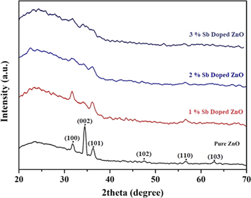
Figure 2. XRD patterns of pure and Sb doped ZnO thin films.
Download figure:
Standard image High-resolution imageTable 1. Some calculated XRD parameters of pure and Sb doped ZnO thin films.
| Sample | hkl | 2θ (°) | FWHM (degree) | D (Å) | d (Å) | δ ×10−3 (1/Å2) | ε | Microstrain (×10−3) |
|---|---|---|---|---|---|---|---|---|
| ZnO | 100 | 31.770 | 0.265 | 346.9 | 2.814 | 2.883 | 0.237 | 4.106 |
| 002 | 34.473 | 0.275 | 336.0 | 2.599 | 2.976 | 0.222 | ||
| 101 | 36.439 | 0.,335 | 277.4 | 2.464 | 3.305 | 0.254 | ||
| ZnO: Sb (1%) | 100 | 31.781 | 0.231 | 397.7 | 2.813 | 2.514 | 0.203 | 14.273 |
| 101 | 36.462 | 0.339 | 278.2 | 2.462 | 3.647 | 0.257 | ||
| ZnO: Sb (2%) | 100 | 31.832 | 0.504 | 181.9 | 2.818 | 5.500 | 0.442 | 14.424 |
| 101 | 36.403 | 0.218 | 426.5 | 2.466 | 2.345 | 0.165 | ||
| ZnO: Sb (3%) | Could not be measured because it is an amorphous structure | 83.194 | ||||||
The crystal sizes of the structures from the peaks in the graphs Debye-Scherrer's formula calculated by equation (3).

Where D is the mean size of the ordered (crystalline) domains, which may be smaller or equal to the grain size and its unit is Å, K is a dimensionless shape factor, with a value close to unity. The shape factor has a typical value of about 0.89, but varies with the actual shape of the crystallite; β is the line broadening at half the maximum intensity (FWHM), after subtracting the instrumental line broadening, in radians and θ is the Bragg angle. While (002) direction plane crystals disappear for doped ZnO thin films, the crystal size of the thin films generally increased with Sb doping for (101) plan up to 2%, and it firstly increases and then decreases for (100) plane. The crystal size of the 3% Sb doped thin films could not be measured because of its amorphous structure. The bond lengths that are adjacent to the Sb atom are longer than the Zn atom. This causes microstrains or dislocations in that position.
Dislocation density (δ) defined as the length of dislocations lines per unit volume was calculated by

The strain produced in the samples due to Sb doping was calculated using the relation [29]

Table 1 shows that the microstrain is naturally present only in the ZnO structure. This value increases according to the contribution rate. This increase is due to the fact that the atomic radius of the atom Sb is greater than the atomic radius of the atom Zn.
The portions a, b and c shown in figure 3 are similar to the Sn doped ZnO example in the study by Yang et al. The lattice parameters belonging to undoped and Sb doped ZnO crystals (compared with Reference ZnO [30] were given in table 2. The crystal system for all the samples here is the hexagonal and space group P63mc. The radius of the Sb atoms is higher than Zn atoms. Therefore, the bond length of Sb-O is higher than the Zn-O bond length [31, 32]. It increases the unit cell lengths and unit cell volume. In figure 3, the placement of the molecule and the addition of Sb to the unit cell was given as given by the hexagonal structure as given. In figure 3(d), three wurtzite cells were plotted in a hexagonal structure. That is to say, a combination of a wurtzite cell and a hexagonal cell is formed. The definition of this is the wurtzite solution on the hexagonal base. Therefore, the settlement and the plane indices of the main atomic peak, shown in figure 3 is shown in the wurtzite cell [33].
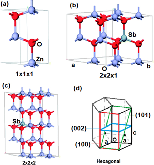
Figure 3. Possible unit cell placements for ZnO and Sb doped ZnO.
Download figure:
Standard image High-resolution imageTable 2. Lattice parameters of ZnO and Sb doped ZnO thin films.
| Sample | Reference ZnO [32] | %0 Sb:ZnO | %1 Sb:ZnO | %2 Sb: ZnO | %3 Sb:ZnO |
|---|---|---|---|---|---|
| Crystal System | Hexagonal | Hexagonal | Hexagonal | Hexagonal | Hexagonal |
| a = b (Å) | 3.22 | 3.2442 | 3.2452 | 3.2585 | 3.2608 |
| c (Å) | 5.2 | 5.2055 | 5.2661 | 5.2745 | 5.3020 |
| α = β | 90° | 90° | 90° | 90° | 90° |
| γ | 120° | 120° | 120° | 120° | 120° |
| Cell volume (Å3) | 46.700 | 47.448 | 48.029 | 48.501 | 48.821 |
| Space Group | P 63 m c | P 63 m c | P 63 m c | P 63 m c | P 63 m c |
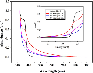
The optical properties of pure and Sb-doped ZnO films were investigated using the absorbance-wavelength measurements in the range of 300–900 nm at room temperature. Figure 4 presents the absorbance of pure and Sb doped ZnO films prepared at different doping ratios. The energy band gaps were determined by the following equation:

where α is the coefficient of absorption, β is an energy-independent constant, m is ½, hν is the incident photon energy, and m is a constant which defines the type of optical transitions for an indirect allowed transition or allowed transition.
Figure 4. Absorbance-wavelength and (Ahν)2-Energy plots of ZnO films for different Sb doping ratio.
Download figure:
Standard image High-resolution image
The band gap energy for all the thin films found to be 3.26 eV (with no doping), 3.05 eV, 2.92 eV, and 3.09 eV (correspond to with 1, 2 and %3 Sb doping, respectively) which can be attributed to the low band tailing effect and defects such as interstitial zinc atoms [34]. Results were indicated that the Sb dopant displays a band gap decrease, which has significant for optoelectronic devices applications [35, 36]. Benelmadjat et al noted that the optical band gap of Sn doped ZnO thin films was influenced by the nature of dopant used. Sn dopant decreases the optical band gap until 3.30 eV for a doping rate of 7% in solution, which is because of the ionized donors [21]. Yung et al showed that the band gap of Sn doped ZnO films reduce from 3.38 to 3.18 eV with an Sn dopant [37]. Mendoza et al studied the optical properties of Al, Ag, Sb, and Sn doped ZnO films by ultraviolet-visible spectroscopy. They showed that the band gap of ZnO thin films increases with Al ion doping and reduces with metal (Ag, Sb, and Sn) ions [38].
4. Conclusion
In summary, pure and Sb-doped ZnO films grown by spin coating technique were investigated by fabricating them onto the SLG substrate. All of SEM images were strongly effected depending Sb doped increase. Pure and 1% Sb doped ZnO film showed a nanofiber structure. The XRD patterns indicated that ZnO film and Sb doped ZnO films have highly oriented polycrystalline. The band gap energy for all the thin films changed between 3.26 and 2.92 eV related to the Sb dopant. The band gap energy for all the thin films profoundly changed as Sb contribution increased.