


Abstract
This paper demonstrates variable frequency microwave processing of silver nanoparticles inkjet-printed onto polyethylene terephthalate (PET) substrate. Printed patterns were in situ monitored with the use of a camera and specially developed two-color infrared pyrometer. It was demonstrated that direct microwave heating of metal inks is very challenging to control due to the progressive evaporation of polar solvents, and almost always leads to non-uniform heating and significant sample deformation. To overcome this difficulty, a PET-based substrate with a solvent-absorbing layer was used. Samples were analyzed at various heating periods and microwave power levels. The collected results reveal a sharp increase in the temperature at the very first moment of the microwave irradiation caused by concomitant interaction with electric and magnetic fields. Depending on the processing conditions, the sintered samples achieved relatively low electrical resistances at the very beginning of the irradiation periods. The lowest measured resistivity was about 30  cm after only 5 s of irradiation. Microstructural analysis of the film revealed inter-particle neck formation and no significant grain growth. The observed reduction in the electrical resistivity upon microwave irradiation was mainly ascribed to the neck formation and its progressive growth.
Export citation and abstract BibTeX RIS
1. Introduction
Recent progress in the development of wearable devices, flexible sensors, lighting, and photovoltaics combined with novel cost-effective manufacturing onto various flexible substrates including plastic, paper or textiles makes this a very active field of research. In contrast to manufacturing methods for silicon devices where rigorously controlled conditions and several sophisticated steps are involved, printing technologies provide additive deposition of functional inks in ambient conditions at less expense and with significantly high-throughput fabrication processes for flexible electronics. Inkjet printing is commonly utilized because new electronic devices can be printed with a significant reduction of material waste. Currently, high-resolution inkjet printing of metal inks is used for the fabrication of electrodes or antennas. These inks are usually formed of nanoparticles (NPs) surrounded by an organic stabilizer and dispersed in solvent vehicles that meet the rheological properties necessary for inkjet printing. Once printed, the inks require a heat treatment generally above 150 °C for several minutes in order to remove organic compounds as well as sinter metal nanoparticles for better electrical conductivity. This post-printing step becomes challenging with the use of low-cost polymers like polyvinyl chloride or polyethylene terephthalate (PET) as a substrate. These materials exhibit low thermal stability and glass transition temperature (Tg) below 100 °C. Heating in a standard oven results in their thermomechanical deformation which can result in cracks and delamination of the printed patterns. Thus, alternative approaches are imperative and sintering with laser, [1–4] infrared, [5–7], microwaves [8, 9] and photonic curing [10–13] methods are all being actively investigated. Most of these techniques are based on absorption of the electromagnetic field energy that leads to rapid heat generation in the printed metal films. Since the microwave heating enables both rapid processing and volumetric heating, this method is of particular interest for applications to fast sinter various materials including metal micro- and nanoparticles. Although bulk metals are known to be reflective at microwave frequencies, Roy et al [14] were the first to demonstrate that powdered metals can be heated and thus densify by microwaves. Later, Ma et al [15] reported a systematic study of the microwave absorption and heating behavior of compacted copper microparticles. With the use of a single-mode microwave system, they demonstrated how the processing in pure electric (E) or magnetic (H) fields influences the heating trends and final electrical properties of the investigated samples. Their results showed that electrical conductivity can be achieved either in E and H field within few seconds. Moreover, they noticed a short but significant temperature rise at the very beginning of the microwave irradiation. While the previous studies had presented microwave heating for metal compacts made of microparticles, Perelaer et al [8] were the first to demonstrate the microwave sintering of silver nanoparticles (AgNPs) for application to printed electronics. They showed that, in contrast to 60 min required for the conventional heating, with the use of microwave single-mode cavity (2.45 GHz) the processing time of AgNPs patterns printed onto polyimide (PI) substrate was reduced down to about 4 min or even down to 1 s [9]. Nevertheless, it was pointed out that a particular pattern design (antenna) in the proximity of samples (lines) was required to facilitate microwave absorption.
In the present study, we demonstrate and discuss microwave sintering of AgNPs inkjet-printed on PET substrates. Unlike the previously reported work, the printed patterns are sintered in a multimode cavity with a variable-frequency-mode (VFM) microwave generator operating at a central frequency of 6.425 GHz. Comparing to fixed-frequency systems, the VFM generators furnishes a more uniform EM field distribution inside the microwave cavity and thus renders a more homogeneous heating. In order to understand the overall outcomes of the microwave heating process, an experimental setup including a charge coupled device (CCD) camera and a customized infrared two-color pyrometer was built and installed on the top of the microwave cavity. The pyrometer developed specially for this study provide on-line high-speed temperature measurements regardless of emissivity changes and has full-scale (350 °C) accuracy error of about 3%. The camera allowed real-time observation of the printed patterns at different stages of the heating process.
2. Materials and methods
2.1. Sample preparation
An ink (Suntronic U5714, SunChemical) containing 40 wt% of AgNPs with the particle diameter ranging from 20 to 50 nm was used for preparing 1 cm × 1 cm square patterns (figure 1). The exact composition of the ink is considered proprietary by the manufacturer, nevertheless based on available data it is believed that the AgNPs were encapsulated with a polymer and dispersed in a mix of polar solvents composed of ethanol, ethylene glycol, and glycerol. Printing was performed in a drop-on-demand inkjet printer (DMP-2800, Fujifilm Dimatix). Depending on the experiment, the ink was deposited onto one of two different types of transparent PET substrates. The first one was a glossy thermostabilized, a 125 μm thick PET (Lumirror® 60.28, Toray). The second one was a 140 μm thick PET, with an ink-receptive mesoporous coating (Novele IJ-220, Novacentrix). This ink-receptive layer quickly absorbs the solvents and an initial electrical conductivity of printed patterns can be achieved without any drying process. Although the electrical conductivity of these prepared patterns was very low, by omitting the drying step, total processing time can be significantly reduced. Nevertheless, in order to improve the conductivity of the printed samples, a sintering was still required.

Figure 1. Samples of square patterns inkjet printed onto mesoporous PET substrate.
Download figure:
Standard image High-resolution image2.2. Experimental setup for microwave processing
All the experiments were carried out in a microwave multimode cavity (Microcure 2100, Lambda Technologies). The cavity was connected via rectangular C-band waveguide to a variable frequency generator. The generator was set to operate at a central frequency of 6.425 GHz with a sweeping bandwidth of 1.15 GHz. The sweep time was set to 1.25 s, and the applied power was tuned from 10 to 500 W for specific items. The microwave processing of the printed patterns was in situ monitored with the use of CCD camera (TM-4200GE, JAI) and specifically developed pyrometer. The camera and the pyrometer were located outside the cavity and were pointed at the sample through a microwave choke that was carefully designed in order to avoid the microwave leakage outside the cavity. Illustration of the experimental setup is presented in figure 2.
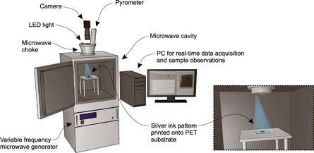
Figure 2. Illustration of the experimental setup.
Download figure:
Standard image High-resolution image2.3. Temperature measurement
2.3.1. Principles of the radiometric temperature measurement
The principle of operation of the radiometer-pyrometer sensors has already been extensively described in details in the past [16, 17]. In short, typical pyrometers are equipped in a narrow band photodiode (PD) embedded with an amplifier circuit. These PDs generate photocurrent (I) proportional to the intensity of thermal radiation emitted by an investigated object in the narrow spectral band corresponding to its spectral response with maximal sensitivity wavelength according to the modified Planck's formula (equation (1)).
where  ,
,  ,
,
- I—photocurrent (nA) (registered by the photodiode),
- C1 and C2—radiation constants in the Planck's law (
 ),
), - K—factor defined by the specific electronic circuit and the optical scheme,
 —emissivity of an object,
- λ—maximal sensitivity wavelength of a specific photodiode (),
- T—temperature (K).


After an appropriate transformation, the equation (1) can be solved with regard to temperature as follows:

Although the above equation converts simply and accurately the measured photocurrent to temperature, it assumes that the emissivity value is known. In practice, the emissivity varies with the temperature and with the sample surface properties, e.g. roughness changes during the sintering. Owing to the emissivity variations the two-color pyrometers are frequently used. In contrast to the monochromatic sensors, the two-color pyrometers are equipped in two photodiodes that permit to measure the temperature independent of the emissivity changes. The ratio of the photocurrents generated by the two PDs at wavelengths  and
and  is converted to the temperature according to equation (3). Reliable temperature measurements with the use of bichromatic pyrometers state that the emissivity variations have to be the same for both wavelengths, i.e. the ratio between the emissivities variations has to be constant across the entire temperature measuring period according to equation (3).
where  , (
, ( and
and  correspond to specific wavelengths of different photodiodes in the pyrometer),
 ,
,
 , (B1 and B2 are B in the equation (1) with corresponding factors related to channels '1' and '2' of the pyrometer).
2.3.2. Description of the bichromatic pyrometer developed
The optical schematic of the pyrometer was designed in such a way that the thermal radiation emitted by the investigated sample was registered at a circular spot that has 1 cm in diameter. The temperature was calculated on the basis of the thermal radiation energy measured on that spot. Illustration and an optical schematic of the pyrometer are shown in figure 3. The thermal radiation from the sample is focused by a sapphire lens (diameter D = 25.4 mm, focal length F = 50.8 mm, Edmund Optics) on a silicon beam splitter (400 μm thick silicon plane mirror set at an angle of 45°). The beam splitter divides the radiation coming from the object with a ratio of about 1:1.5. After the signal division, two photodiodes (PD42Su,  = 4.15 ± 0.2 μm and PD34Su,
  = 3.25 ± 0.15 μm, IoffeLED, Ltd.) were used to collect the thermal radiation. The greater part of the registered radiation is directed to the PD42Su photodiode that produced about 1.5–2 times greater electrical noise. Thus, the accuracy signal-to-noise ratio (SNR) for both PDs is almost the same.
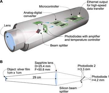
Figure 3. (A) Illustration of the developed pyrometer and (B) its optical schematic.
Download figure:
Standard image High-resolution imageThe selection of the PDs follows from the fact that for the radiometric-pyrometric measurements the largest responsivity to the temperature changes can be achieved with the wavelength-temperature product (λT) close to about 1500 (μm K). This relation applied to low-temperature pyrometry (below 400 °C) defines optimal wavelengths to be in the middle infrared (mid-IR) spectral range (λ = 2–5 μm). Note that the selection of the PDs wavelengths  and
and  should be chosen far apart in order to minimize the error in the temperature measurements that is related to the variation of emissivities (
 and
and  in equation (3)). However, the detectivity (D*) and the SNR must be also maximized for better accuracy. Finally, the desorption of gaseous species like hydrocarbons during the heating has to be taken into account. They may alter the measured signal because of a partial light absorption. The specific parameters of the selected immersion lens PDs, as well as an example of measuring error, has already been described by Sotnikova et al [17].
To ensure thermal stability of the PDs, each of them was mounted on a thermoelectric cooling module. The temperature was stabilized at 20 ± 2 °C. The photocurrents from PDs were amplified with a transfer coefficient  and transferred to a two-channel 12 bit analog-digital converter (ADC) operating at a fixed frequency of 30 KHz (sampling rate of about 30 kS s−1), which provides high-speed data acquisition, suitable for monitoring of fast microwave heating processes. Digital data corresponding to both channels of the pyrometer were real-time transferred with an Ethernet cable to the PC for further calculations. The housing of the pyrometer was equipped with a laser pointer in order to facilitate positioning of the sample with the area scanned by the pyrometer. During the temperature measurements, a geometrical center of the printed pattern (1 cm × 1 cm) was superposed with the center of the pyrometer's measuring spot.
2.3.3. Calibration of the pyrometer
The both channels of the two-color pyrometer were calibrated with a black body (BB) (BB703, OMEGA). The temperature of the heat source was increased with a constant rate of 1 °C min−1. The measured values of photocurrents and the temperature of the BB calibrator were registered simultaneously. The calibration curves presented in figure 4 match the BB model (fitted based on the equation (1) with = 0.95) from about 70 °C. It defines the lower limit for the temperature measurements. The highest temperature that can be measured by our pyrometer was about 350 °C. At that temperature, the thermal radiation of the heat source ( = 0.95) causes saturation of signal measured by the PD sensitive at λ = 3.25 μm. This signal saturation is related to the resolution of the ADC (12 bit). An extension of the upper-temperature limit would be possible if higher resolution ADC is implemented. The developed two-color pyrometer was intended to be used for real-time temperature monitoring of samples printed on various plastic substrates that are usually heat-sensitive and thus the operating temperature range was sufficient.

Figure 4. Calibration curves of the developed pyrometer.
Download figure:
Standard image High-resolution image2.4. Loss tangent—method of measurements
The ability of polar solvents to heat under microwaves is characterized by the loss tangent (tan δ) defined by equation (4). For efficient microwave heating, a moderate value for  should be combined with the high value of
  .
.

where  —real permittivity characterizing the penetration of microwaves into the material,
  —loss factor indicating the material's ability to store the energy.
A vector network analyzer equipped with a dielectric probe kit (85070E, Agilent) was used to measure  and
and  of the materials investigated. Silver ink as well as a blend of solvents (mainly ethylene glycol, ethanol, and glycerol) with the same chemical composition as the ink but without the AgNPs, were analyzed under various temperatures and frequencies.
During the measurements, test-tubes were filled with about 1 ml of each of these materials, so that the volume was enough to immerse the test probe. The loss tangent of distilled water was additionally measured and demonstrated as a reference to the analyzed materials.
3. Results and discussion
3.1. Loss tangent—analysis of the investigated materials
The frequency-dependent loss tangent (tan δ) analysis at 25 °C, 80 °C, and 125 °C, is presented in figure 5. The results exhibit no significant differences between the ink and the blend of solvents. At room temperature, both mixtures reach maximum tan δ values at a frequency (fmax) of about 2.45 GHz. The increase in the temperature causes a shift in fmax toward higher frequencies. This phenomenon has been already reported by Lou et al [18, 19] and was ascribed to decrease in solvent viscosity at higher temperatures.
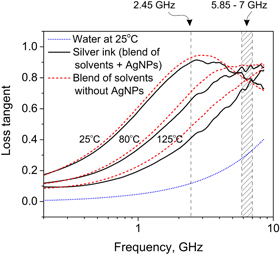
Figure 5. Loss tangent changes for the materials investigated at various temperatures as a function of frequency.
Download figure:
Standard image High-resolution imageThe similar changes of the loss tangent for the both analyzed mixtures indicates a negligible impact of AgNPs on the microwave absorption and thus the microwave heating. The values of the tan δ are mainly related to the dielectric properties of the polar solvents mixture. Within the operating frequency range of the microwave generator (5.85–7 GHz), the loss tangent at three different temperatures exhibits a relatively high value of about 0.8 and confirms the ability of the ink to high microwave absorption.
3.2. Microwave processing of printed ink onto glossy PET substrate
Microwave heating of a printed silver square pattern on the glossy PET substrate is demonstrated in figure 6. The progress in solvent evaporation was in situ monitored by using the CCD camera. Although the applied power was relatively high (300 W), about 100 s were needed to observe the onset of solvent evaporation (figure 6(B)). This is because the volume of the inkjet-printed ink layer was very small, and thus the heating efficiency was limited. The total dissipated power per unit volume of a sample related to the heating can be described by the equation (5):

where P is the power dissipation (W cm−3), σ is electrical conductivity (S m−1), E and H are amplitudes of the electric field (V m−1) and magnetic field (H m−1), respectively, f is frequency,  ,
,  ,
,  ,
,  are permittivity of vacuum, relative dielectric loss, permeability of vacuum, relative magnetic loss, respectively. According to this equation, for thin film samples characterized by low electrical conductivity, heat can be efficiently generated if sufficient power is employed. Because the ink is relatively poor electrical conductor interactions with the magnetic field are negligible and thus the last term of the equation can be omitted at the initial stage of heating. It becomes significant once the solvent is evaporated.

Figure 6. Microwave heating of the printed ink on the PET glossy substrate. Samples were in situ monitored by using the CCD camera. The white spots in the images correspond to light reflections (LED diodes) from the sample's surface. The progressive solvent evaporation and the observed deformations cause changes in the surface geometry of the printed pattern and results in strong reflections that partially saturate the 12 bit CCD sensor of the camera. For stronger contrast between the printed ink and the substrate, the images have been modified by adding color masks.
Download figure:
Standard image High-resolution imageAt the beginning of the MW irradiation, we noticed that the solvent evaporation process takes place preferentially at the thinner edges. While the evaporation starts on the sides, the nanoparticles previously separated in the ink are spontaneously brought into contact. Locally, a newly formed layer of AgNPs appears. This layer is electrically conductive and thus began to dissipate the microwave energy more efficiently than the liquid solvents. The energy absorbed by the conducting layer increases as the conductivity augments, causing a subsequent rise in the temperature [20]. The solvents evaporate progressively, until a point (conductivity) is reached where the trend reverses and the microwave field energy is mainly reflected [20, 21]. An illustration of silver nanoparticles at diverse stages of the microwave processing is demonstrated in figure 7. We observed that when the silver layer on the edges forms a closed loop around the central part of the sample (remaining still liquid), a sudden acceleration in the evaporation takes place (figure 6(C)). The closed metal loop is subject to excessive heat generation, few milliseconds after being formed. This effect is probably caused by Joule heating related to the induced eddy currents that occur in conductors under an alternating magnetic field. This spatial non-uniformity of electromagnetic field distribution within the sample (between the metallic edges and the still liquid areas) is liable to cause excessive temperature gradients with localized hot spots. Therefore, the generated thermal stress leads to significant deformation, cracks and even local melting spots in the sample (figures 6(D)–(F)).
Consequently, the direct microwave sintering of silver nanoparticles from colloid ink becomes challenging. In practice, a feedback control system has to be developed where the forward power level can be automatically dropped down as the sample's temperature suddenly surges. Nevertheless, the non-uniform spatial heating makes it difficult to measure the overall temperature accurately. Another possibility for the microwave curing process is to use a so-called susceptor that may dissipate the microwave field energy. Although the susceptors are typically made of materials that absorb the microwave energy very efficiently, like silicon-based materials, usually, they cause excessive heat generation. For this reason, susceptors are not suitable for use in the proximity of the heat-sensitive plastic substrates. The damages and large sample's deformation seem to be inevitable in the present configuration of the microwave heating system. Alternatively, the printed patterns can be dried prior to the sintering process or an ink-receptive substrate that quickly absorbs the solvents can be used.
3.3. Microwave processing of printed pattern onto mesoporous PET substrate
To overcome the problem related to the sudden and non-uniform overheating of the silver ink and the resultant deformations, a PET substrate with an ink-receptive mesoporous coating was used. The exact composition and relevant information on the PET coating material are kept confidential by the manufacturer. However, based on the data available, its composition is believed to contain some acidic or anionic coating that facilitates the detachment of the organic layer surrounding the nanoparticles. Moreover, Kang et al [12] analyzed this porous layer using SEM which reveals pore size of about 22 nm. Thanks to the porosity, the solvents were absorbed almost immediately resulting in a low-conductivity metallic thin film without any thermal treatment. The dry thin metallic film had relatively high resistivity of about 4000  cm and its processing was still required in order to improve the electrical conductivity.
Now we thoroughly detail how the microwave irradiation parameters relate to the thermal response of the metal films and impact their final conductivity. During the processing, the samples were in situ monitored by using the experimental setup described in figure 2. Figure 8 demonstrates a set of data registered during each experiment of the microwave heating. For a given applied power, a thermal response of the printed pattern was registered as an evolution of photocurrents at the two wavelengths of the photodiodes. The temperature was real-time and automatically calculated using equation (3) with a relative emissivity ratio set to 1.
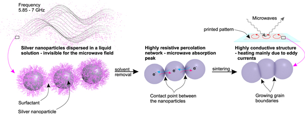
Figure 7. Illustration of the silver nanoparticles at diverse stages of microwave processing.
Download figure:
Standard image High-resolution imageFirst, in order to check for reproducibility of the thermal response of the samples under the microwave exposure, the processing time was varied at two fixed power levels (200 and 300 W). The resulting thermal profiles are shown in figure 9. We noticed almost identical trajectory of the collected results what indicates on high repeatability of the microwave heating process. Next, the samples were investigated at five different power levels ranging from 100 to 500 W (figure 10). At the very beginning of the microwave irradiation and for all samples, we observed very fast heating rates (over 100 °C s−1) up to certain temperature levels depending on the power selected. The as-printed layer made of silver nanoparticles exhibits low electrical conductivity which leads to strong microwaves absorption. This results in a significantly increased Joule heating by the concomitant of loss current by free charge carrier in the material under E field and eddy current induced by the alternating H field (see equation (5)). Ma et al [15] suggested that the strong microwave absorption by copper powder compact is attributed to the ohmic heating by the skin effect as the size of microparticles is much smaller than the skin depth. In the present study, the skin depth was in the micro-scale which is far greater than the mean diameter of AgNPs.

Figure 8. Set of data registered during each experiment and real-time conversion of the photocurrents to temperature.
Download figure:
Standard image High-resolution image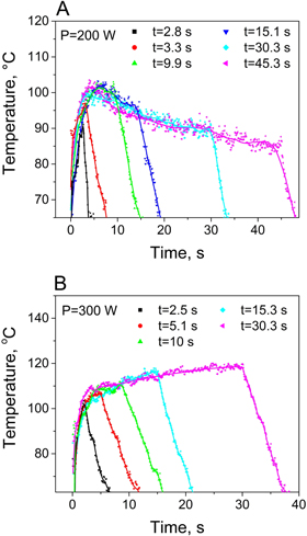
Figure 9. Comparison between thermal cycles for various microwave heating time and constant applied power. (A) P = 200 W, (B) P = 300 W.
Download figure:
Standard image High-resolution imageMicro-focusing effect by E and H field occurring in small particles can also be responsible for the considerable heating rate at the initial stage [22]. This effect describes the intensification of the externally applied field in the neck region between two touching particles, resulting in a large absorbed energy at the interface between these particles.
As the temperature increases rapidly, the film undergoes microstructural evolution since sintering process promotes inter-particle neck growth and lead to improvement in the electrical conductivity upon a certain limit. At this step, the induced E field magnitude decreases in the film resulting in a reduction of the absorbed power density from the electric field. On the other hand, the eddy current density related to ohmic heating, expressed as  (where E is the electric field induced H field and σ is the electrical conductivity), is enhanced with increasing the electrical conductivity. Thus, the ohmic loss by eddy current became dominant heating mechanism. The heating rate is slowed down at this second stage of heating as the electric field is reflected by the film. With the improvement in electrical conductivity of the silver film its thermal conductivity increases. It leads to thermal losses of the generated heat to the surrounding environment. Therefore, for the applied power below certain level (in this work about 300 W) heat generation is compensated by thermal energy losses and in spite of continuous irradiation the temperature slowly decreases.

Figure 10. Thermal profiles of the silver nanoparticles thin film during microwave heating at various power levels.
Download figure:
Standard image High-resolution imageFinal resistivities of the patterns were measured using van der Pauw method [23], the results are shown in figure 11. We observed that the most significant improvement in the electrical conductivity occurs at the very beginning of the irradiation. This is in accordance with the fast heating rates that occur at the first stage of the microwave processing. The resistivity decreases significantly with applied power and then tends to stabilize regardless the irradiation time. Analysis of film microstructures by SEM reveals no significant differences between the samples heated at various power as no evident grain growth was observed (figure 11). The improvement in the electrical conductivity is mainly due to inter-particles neck growth during the initial short microwave heating periods, which is probably assisted by the micro-focusing effect as discussed above.

Figure 11. Evolution of the resistivity and microstructures for various combinations of microwave irradiation periods and applied power levels.
Download figure:
Standard image High-resolution image
The stabilization of resistivity is in accordance with the establishment of film microstructures. This confirms that the second heating stage observed for powers above 200 W does not imply significant film modification. The lowest measured resistivity of 30  cm was obtained at 500 W in less than 5 s, which is 18 times higher than that of the bulk resistivity of silver. Increasing the irradiation time at 500 W improves the electrical conductivity of samples, however their thermomechanical deformations have been visually observed.
4. Conclusion
The variable frequency microwave irradiation of silver nanoparticles-based ink was investigated. An original experimental setup with a customized bichromatic pyrometer was built. It can provide thermal and visual in situ monitoring of the samples during their entire microwave irradiation process. The customized pyrometer, thanks to its bichromatic sensitivity, can measure the temperature of a thin silver film in spite of its low emissivity and the emissivity changes that take place during the heating.
Direct processing of the silver ink printed on the glossy substrate leads to sudden acceleration of the heating process and significant thermal gradient while the solvents evaporate. Localized hot spots were observed provoking large thermomechanical deformations. In order to avoid such deformation, it is necessary to dry the ink prior to the sintering process or to use an ink-receptive substrate with a porous coating that quickly absorbs the solvents. In this work, we used the ink-receptive substrate that besides the high absorption capacity for fluids, provides excellent adhesion with the printed patterns. It should be noted however that with the porous coating, the adhesion of entire printed pattern mainly depends on the adhesion strength between the PET and the porous layer (holding the printed pattern).
Systematic studies carried out with the samples printed on the ink-receptive PET substrate reveal rapid heating rates at the very beginning of the microwave irradiation, regardless the applied power. Joule heating by both electric and magnetic field seems to be the major cause of heat generation at the first stage. The enhancement in electrical conductivity during microwave processing tends to reflect the electric field what results in less violent heating rates after the first seconds of irradiation. Nevertheless, the heat can still be generated by eddy currents losses induced by the magnetic field. The balance between the thermal losses and the generated heat defines the second stage of the thermal profile.
Although in this work we demonstrated sintering of silver square samples, the microwave processing is suitable for curing of other patterns like for example lines. The square patterns were chosen only due to the temperature measurement with the pyrometer that measures the thermal radiation on a circular spot of 1 cm (similar to dimensions of the printed sample). With fine line patterns, an accurate temperature measurement would be difficult.
The variable frequency microwave irradiation carried out in the multimode cavity was demonstrated to be an effective and fast heat treatment method. The resistivity of 30  cm was achieved at 500 W in less than 5 s without any thermomechanical deformation of the substrate. Analysis of film microstructure reveals no evident grain grows and shows mainly inter-particles necks contacts that reduce the electrical resistivity of the investigated samples.
Although with the use of the analyzed materials and configuration of the experimental setup, significant improvement in the electrical conductivity seems to be difficult, this does not demarcate the limit for optimizing microwave processing of printed metal inks. Future work might include the development of VFM furnace with high power microwave pulses, and thus with a capability of generating heat in very short time (milliseconds). Also, the integration of infrared lamps for ink drying inside the microwave cavity could help improving heating uniformity.
Acknowledgments
The authors acknowledge the help of M Remennyy, A Lavrov and S Karandashev in the development of the pyrometer.