Abstract
Abstract not Available.
Export citation and abstract BibTeX RIS
On the occasion of the fiftieth anniversary of the Electrochemical Society in 1952, William Blum published a review on electrodeposition in which he regretted that its theoretical basis was largely insufficient and "the great advances that have been made in electrodeposition are therefore largely empirical." 1 Twenty-five years later, Mc Kinney and Faust2 published a follow up report in which they presented a detailed account of many technological advances achieved during that period. From today's perspective, it is interesting to note that the authors mentioned electronics applications just briefly, and they devoted only a single paragraph to fundamentals. Apparently, electrodeposition was still perceived as a mostly empirical technology serving primarily for surface finishing and corrosion protection. Of course, electrochemists and electrochemical engineers had studied the scientific principles governing plating processes for many years before, and an impressive amount of knowledge was available. However, it would seem that this knowledge had not yet made a decisive industrial impact. At present, the situation has dramatically changed. Some of the most advanced experimental and theoretical modeling work in electrochemical metal deposition and dissolution is performed in industrial research laboratories and electrodeposition and dissolution processes have found a firm place in electronic device fabrication.3
Electrodeposition as an industrial activity has been practiced for over 150 years, one of the first applications having been the electroforming of printing plates.4 Subsequently, electroplating gained major importance as a cheap and versatile surface finishing process for decorative applications and for corrosion and wear protection. Typical examples include chromium plated automobile trimmings, gold plated brass jewelry, nickel-plated steel, gold plated electrical contacts or hard chromium plated bearings. Traditionally, the automotive industry has been a big user of electroplating (Fig. 1).5 While this industry used large integrated plating facilities, much of the plating for other applications was performed by specialized shops of relatively small size. Indeed, a characteristic of the traditional plating industry has been its fragmentation to which several factors may have contributed. On one hand, before strict environmental regulations came into effect, the investment needed to start a commercial plating activity was relatively modest. Furthermore, the availability of fully formulated commercial plating electrolytes reduced the development efforts needed to start production. Success of a plating operation then depended mostly on the skill and ingenuity of the electroplater. Because electroplating depended largely on empirical know-how and involved handling of aggressive chemicals and solutions, it did not fit well into mechanical production lines and many manufacturing industries preferred to subcontract plating operations to specialists. At the end of the twentieth century though, the electroplating industry is undergoing fundamental changes, which are likely to continue in the future.
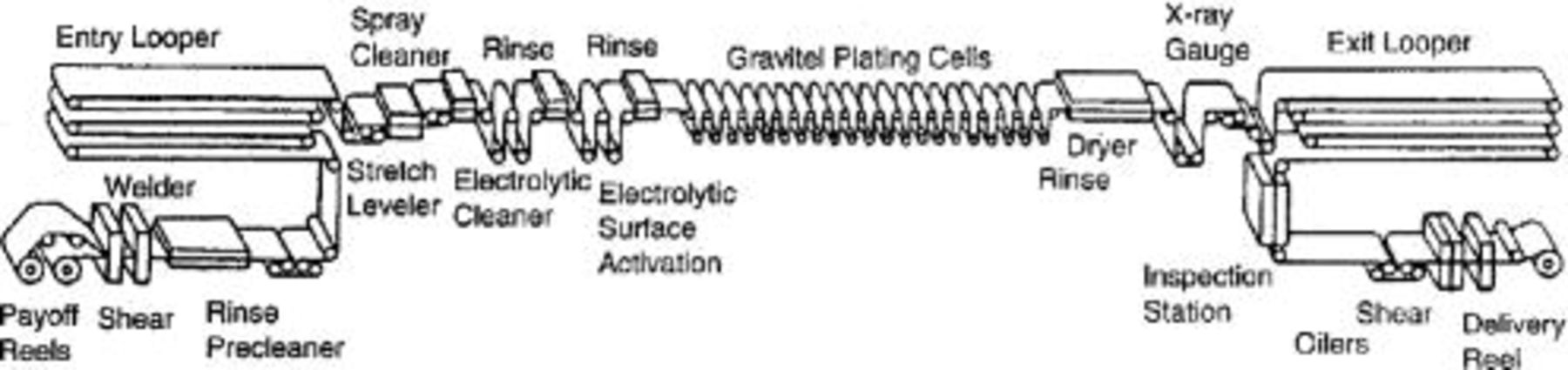
Figure 1. Corrosion of automobile body panels has been drastically reduced by the introduction of zinc and zinc alloy coated steel sheet. Fully automated plating lines have been designed to produce coated steel sheet at a fast, continuous process. The figure shows a high throughput reel-to-reel zinc plating installation where the steel strip moves at a speed of up to 137 m/min.10
On one hand, due to ever more severe regulations concerning the emission and final disposal of heavy metal ions and chemicals, the electroplating industry today needs advanced water recycling and purification schemes that drastically increase investment cost. Environmental pressures also require that certain established plating processes be substituted by more environment friendly technologies that often require closer control and better scientific understanding. A well-known example is the replacement of cadmium coatings for corrosion protection by other metal or alloy coatings. Hexavalent chromium widely used for chromatation of zinc and in chromium plating has come under attack, as well as lead containing electroplated solder alloys. On objects that enter into contact with the human skin, notably jewelry and watches, traditional nickel barrier coatings must be replaced, because nickel causes allergic reactions in some people. A second driving force for change is the emergence of electrodeposition as a large scale manufacturing process involving fully automated high throughput installations. Examples are found in the steel industry and in the electronics manufacturing industry. In these and other applications electrochemical processes compete with dry processes and to be competitive they must exhibit the same degree of reliability and control. Interestingly, the principles governing scale up and scale down of electrodeposition processes are perhaps better understood at present than those of competing plasma deposition processes. Finally, the general trend towards globalization modifies the market conditions for the electroplating industry and creates new types of partnerships between the manufacturing companies and their subcontractors with ever higher demands on technical competence, cost effectiveness and product reliabilitiy.
The period covered by this report coincides with the emergence of information technology, the first personal computers appearing on the market in the late 1970s and early 1980s. They were made possible by the invention of cheap and powerful microprocessors based on integrated circuit technology and of low cost data storage and retrieval systems. The dramatic pace of progress in information technology and its enormous impact on human society is common knowledge. Perhaps not so well known is the fact that electrodeposition and related electrochemical processes have had a decisive impact on the development of computer technology.6 The present review will retrace significant scientific and technical achievements in electrodeposition science and technology made during the last part of the twentieth century, without any claim to completeness. During this period electroplating, historically considered a "black art." 7 has evolved into an exciting field of high technology with numerous new applications and challenges in micro and nanotechnology. Fundamental research carried out by electrochemists, electrochemical engineers and materials scientists made this development possible. Continuing research will permit to sustain it in the future.
Electrodeposition Technology
Decorative and functional coatings
Traditional applications of electrodeposition include decorative and functional coatings, electroforming of three-dimensional objects and plating of printed circuit boards. Many metal winning and refining processes are based on electrodeposition. These and other applications were thoroughly reviewed by McKinney and Faust.2 The fourth edition of "Modern Electroplating" published recently under the auspices of the Electrodeposition Division of ECS gives a comprehensive overview of the current practice of electrodeposition and electroless deposition of different metals and alloys.8
Decorative chromium coatings have been produced by electrodeposition for many years. Traditionally, the automobile industry has been the largest user, but due to changing fashion trends the importance of decorative chromium plating has diminished in this industry.5 On the other hand, electroplating has found new applications in the field of corrosion protection of automobile bodies. Starting in the 1970s, the automobile industry introduced zinc coated steel sheets for body panels replacing plain steel. In response to the new demand, the steel industry developed high throughput continuous reel to reel plating installations for the production of coated steel sheet.9 10 Metallic Zn or Zn-Ni alloys are plated on one or on both sides of the steel sheet.5 Apparently, the introduction of Zn coated steel was delayed somewhat by the fact that the salt spray corrosion test which has been widely used in industrial corrosion testing, initially indicated poorer performance of Zn coated than untreated steel.11 More realistic tests had to be developed to get better agreement with field experience which showed that the use of zinc coated steel panels drastically reduced perforation of automobile body panels by rust.
Hard chromium coatings plated from chromic acid electrolytes are extensively used for wear protection of bearings and other machine elements. Since hexavalent chromium is believed to be carcinogenic, alternatives have been sought in recent years. Sputter deposited ceramic coatings are a possible alternative for many tribological applications. Electroless nickel-phosphorous coatings are also widely used for corrosion and wear protection. Electroplated nickel-tungsten alloys or chromium plated from trivalent chromium electrolytes have been investigated as alternatives to hard chromium, but as of now have not had a major commercial impact. The automobile industry uses electroplated Ni/SiC dispersion coatings for wear protection of cylinder linings and piston rings in car engines. These materials were originally developed in Germany for the Wankel motor and they were introduced in car engines between 1978 and 1980 in Europe and Japan.12 Electroless Ni-P/SiC composite coatings find many applications in different kinds of machines similarly as electroplated Ni/SiC coatings. Self-lubricating metal matrix composite coatings such as Ni-P/PTFE fabricated by electroless plating are used in the mechanical and process industries for valves, injection molds or sliding contacts.13
Electrodeposited noble metal coatings made of gold, silver, platinum, rhodium and their alloys are extensively used for decorative purposes in the watch and jewelry industries. Gold and gold alloy coatings also serve to avoid corrosion and oxidation of electrical contacts. In the late 1970s and early 1980s the price of gold increased manifold. This led to great efforts to reduce the thickness of gold coatings in electrical contacts or to replace gold by other materials such as silver-palladium and nickel-palladium alloys. In recent years, the price of gold has substantially decreased while that of palladium went up and is now almost twice that of gold. Not surprisingly, the economic motivation for replacing gold with palladium alloys has vanished.
It is well known that only a limited number of metals and alloys can be plated from aqueous solution. The use of organic solvents or molten salts, in principle, should permit to plate a larger number of metals. In Europe a process for fabricating aluminum coatings by electrodeposition from aluminum alkyl complexes in toluene has been brought to an industrial scale.14 Because of technological difficulties and safety issues the process has not found wider application so far. To the authors knowledge no other processes for electrodeposition of coatings from organic solvents or molten salts have gained industrial importance.
Electronics manufacturing
One of the first applications of electroplating and electroless plating in the electronics industry involved the fabrication of printed circuit boards and electrical contacts. Impressive progress recently achieved in these fields include fast speed (several meters per minute) reel to reel plating of electrical contacts and high throughput processing of lead frames. In the 1980s and 1990s electrodeposition and related technologies have found new applications in electronics manufacturing, notably in packaging and magnetic recording. Several recent overviews discuss specific aspects of electrochemical technology in electronics and microsystems manufacturing and the reader is referred to these for more detailed information.3 6 15 16 17 18 19 20 21 22 23 Progress in the field is also documented in several Proceedings Volumes of ECS Symposia, for example references.24 25 26 Compared to competing vapor phase technologies, electrodeposition and electroless deposition offer several advantages for device fabrication. First of all, electrochemical processes are relatively cheap and they are highly selective in that metal is deposited only on those places where it is needed. Electrodeposition has a better throwing power than physical vapor deposition (PVD) and it allows one to produce high aspect ratio structures with good precision. Also, the laws governing scaling up and scaling down of electrochemical processes are relatively well understood. While electrodeposition requires water treatment and recycling installations, the cost of these is not a critical factor for high-throughput production plants.
Of the many applications electroplating has found in electronics, through mask plating of thin film magnetic heads has perhaps had the highest impact. Development of electroplated thin film magnetic heads started at IBM in the 1960s. The process, which included an electroplated permalloy (81 Ni-19Fe) horse shoe magnet and electroplated copper coils was introduced into production in 1979 (Fig. 2).6 17 Continuing progress achieved in through mask plating technology has led to an increase in the magnetic storage density by one order of magnitude every eight years.6 Lately, the rate of growth has accelerated even further due to the development of new magnetic alloys and electroplated combined inductive-resistive heads.21 Progress in through mask plating of magnetic heads has significantly contributed to the fast paced improvement of the performance of modern computers.16
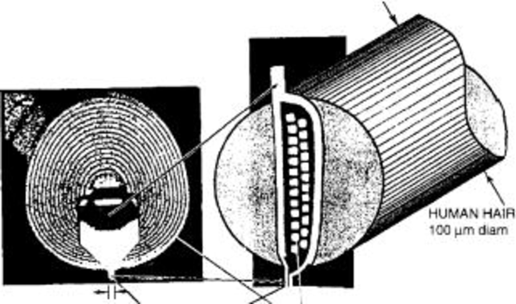
Figure 2. Magnetic recording heads fabricated by through mask electrodeposition were introduced into production in the late 1970s. Continuing miniaturization of electrodeposited magnetic heads has permitted an astonishing increase in storage density ever since. The figure shows an inductive head fabricated by electrodeposition comprising a Permalloy horseshoe magnet and a copper coil. The size of the entire head is comparable to the diameter the human hair shown schematically for comparison.6
Packaging of advanced electronic systems constitutes another important application of electroplating. Packaging serves for signal and power transmission, heat dissipation and for protection against mechanical or chemical damage. A typical packaging hierarchy may include chips, chip modules and printed circuit boards. Advanced computers contain multilevel chip modules, which are connected by fine wiring located on the top of the transistor circuitry of logic or memory chips (Fig. 3).27 In 1997 IBM announced that it would use electroplated copper wiring in advanced IC chips, replacing the vapor deposited aluminum used previously. Compared to aluminum, copper has a higher conductivity and a better resistance to deterioration by electric migration at high current densities. An additional advantage is the easier scalability of electroplating. The electrochemical manufacturing process relies on the so-called damascene plating technology.28 29 Contrary to through mask plating, where metal is selectively deposited into the features of a patterned photoresist, in damascene plating pattern generation precedes the application of a conducting seed layer. Plating is performed on the entire surface and unwanted metal is subsequently removed by chemical mechanical planarization (CMP). Damascene plating permits one to plate simultaneously the via holes and the overlying line trenches (dual damascene plating), making it well suited for interconnect fabrication on an industrial scale. Barrier layer between the seed layer and the insulator prevent unwanted interactions.
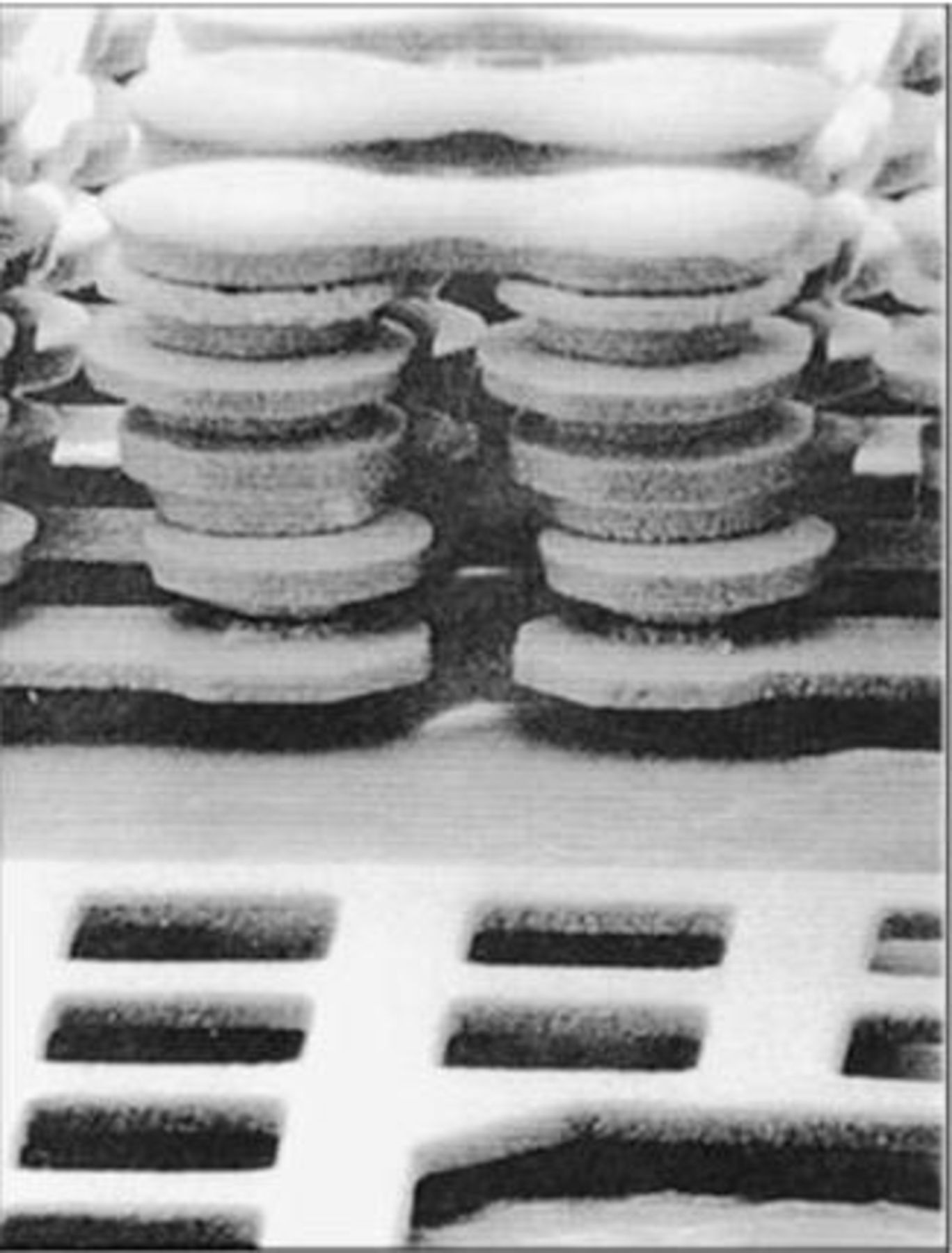
Figure 3. Interconnects are multilevel structures which carry electrical signals between chips in multichip modules. Copper plating is an important technology for the fabrication of interconnects in electronic packaging. The SEM shows a via stack with 11 levels. The experimental structure was fabricated by through mask plating of copper in a number of subsequent steps. For better visibility the dielectric was removed prior to taking the picture.27
Chips must be attached to a substrate. Different technologies compete in this field such as wire bonding, tape bonding or controlled collapse chip connection (4C). The latter technology uses solder bumps, which permit to achieve short interconnection distances for fast signal response and low inductance. In the mid 1990s an electrochemical route for producing lead-tin alloy solder bumps for interconnects was developed.30 The process also includes electroplating of tin-lead alloys as well as a controlled etching step of the seed layers in order to achieve the desired shape of the bumps. Compared to the earlier PVD technology, electroplating presents not only economic advantages but it is also considered to be a more environment friendly technology.28 The reason is that in sputter deposition metals deposit indiscriminately on the reactor walls, whereas in electrodeposition metals deposit only on those spots where they are needed. This reduces the need for cleaning and waste material disposal.
Microelectromechanical systems
Electroforming of three-dimensional structures has been one of the oldest applications of electrodeposition.4 Recent years have seen the emergence of electrochemical fabrication technologies for micro-electromechanical systems (MEMS). For these applications electrochemical through mask plating offers high precision and the possibility to achieve high aspect ratios. The technology has been pioneered in Germany starting in the early 1980s and has become known under the name LIGA, which stands for the German "Lithography, Galvanoformung und Abformung" (Fig. 4). LIGA is a through mask plating process using thick resist masks with high aspect ratio features. Originally, the resists were patterned by X-ray lithography. Through mask plating was performed to produce metallic masters for use in injection molding of precision polymer parts. More recently, high aspect ratio through mask electroplating has been applied to the fabrication of X-ray masks, sensors and tiny turbines among other. Overviews of the LIGA process and similar processes are available,31 32 as well as a discussion of early experimental work on X-Ray lithography performed in the U.S.6 At the time of this writing the indistrial impact of the LIGA process is still limited, but as the technology matures one may expect that many uses will rapidly develop. Resists have recently been developed for LIGA applications, which permit the irradiation with much cheaper UV instead of synchrotron radiation. They allow fabrication of high aspect ratio structures by several subsequent irradiation steps.32 At present, predominantly nickel is used in the LIGA process, but Ni-Fe alloys and copper have also been plated. In the US a complete thin film magnetic micro motor was recently built by through mask electroplating with the aim to demonstrate the outstanding capabilities of this technology.6
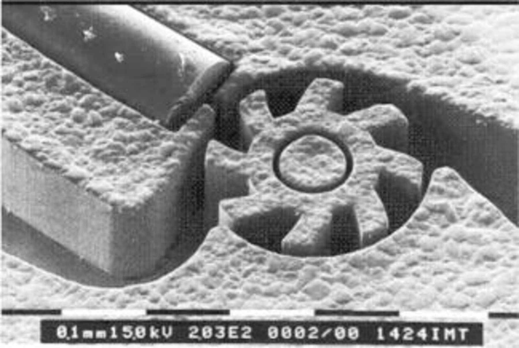
Figure 4. The LIGA process for microelectroforming of metallic components by electrodeposition was developed in the 1980s. Originally synchrotron radiation was used to irradiate PMMA masks suitable for the fabrication of high aspect ratio structures. More recently, UV sensitive resist materials have become available, which permit to achieve similar results without the need for synchrotron radiation. The figure shows an microturbine made by electrodeposition of nickel using the LIGA process. The diameter of the turbine is  Also shown is a glas fiber speed monitor.31
Electrochemical Phase Formation
The kinetics and mechanisms of single metal deposition were studied extensively in the 1950s and 1960s and reaction paths for many systems were established.33 34 Most metal deposition and dissolution reactions proceed through several consecutive steps involving adsorbed reaction intermediates that are often partially hydrolyzed. Complexing species play an important role for the discharge mechanism because they change the thermodynamic equilibrium and the rate determining step of the charge transfer reaction at the electrode surface.33 35 These early investigations laid the foundations for later modeling studies of alloy deposition and additive effects and they provide a solid basis for current studies of electrochemical phase formation using scanning probe techniques. The scientific study of electrochemical phase formation developed in Europe some 50 years ago.36 Of particular interest was the development of a method for the fabrication of almost defect free single crystal electrodes by electrodeposition. It permitted to perform elegant experiments on the energetics of 2D nucleation and to study the role of crystal defects.37 Many authors studied three dimensional nucleation using potentiostatic transient techniques. Formation and growth of three dimensional nuclei on a foreign substrate produce characteristic overshoots in the current transients and their shape can be compared to predictions of theoretical nucleation models. A recent summary of results obtained with this approach is found in Ref. 38. Underpotential deposition (UPD) is another important topic in electrochemical phase formation that has found much attention. UPD implies the formation of a metal monolayer on a foreign substrate at potentials positive to the reversible potential calculated from the Nernst equation. Typically, UPD is observed when the binding energy between the depositing atoms and the substrate exceeds that between the atoms of the deposit material. The phenomenon was observed for the first time in the 1960s.39 The study of UPD became quite popular in the 1970s and 1980s, when several groups used single crystal substrates in combination with linear sweep voltammetry and other techniques for quantifying UPD phenomena. The use of single crystal substrates led to the discovery of the formation of UPD superlattice structures.40 Furthermore, it was found that the nature of the UPD layers depended on the anions present. For more details the reader is referred to recent reviews.41 42 Electrochemical phase formation has been most widely studied on metal substrates, but electrodeposition on semiconductors, notably silicon, is also of great interest, both from a theoretical and from an industrial point of view. The subject has recently been reviewed and three charge transfer mechanisms have been identified, which can lead to electrodeposition of a metal on an n-type semiconductor.43 They involve an electron transfer from the conduction band to the metal ions in solution, the injection of holes into the valence band or an electron transfer from surface states. For a given metal deposit the dominating mechanism depends among other on the prevailing redox potential which can be adjusted by complexing ions.
The invention of the scanning tunneling microscope (STM)44 and of the atomic force microscope (AFM)45 in the early 1980s marked a decisive step forward in the study and understanding of the initial steps of electrochemical phase formation. The STM opened up entirely new possibilities for the observation of the structure of metal-electrolyte interfaces on the microscopic and atomic scales (Fig. 5). The first in situ STM studies of electrode surfaces were published in 1986-88.46 47 48 In subsequent years scanning probe techniques became important tools for the investigation of adsorption on metal surfaces and for electrochemical phase formation.49 50 51 Using single crystals, reconstruction of metal surfaces in solution could be imaged in situ with atomic resolution. For example, the atomic structure of a gold single crystal electrode was found to depend on the applied potential and on the type of anions present.52 The STM also confirmed the existence of super lattice structures deduced previously from indirect techniques. The STM and AFM provided new insight into the role of step and kink sites for electrochemical phase formation and growth. For example, it was found that after formation of an initial UPD layer copper atoms deposit preferentially on monatomic steps of a gold single crystal surface, whereas deposition of silver on the same gold crystal led to a Frank-van der Merve type epitaxial growth up to 10 monolayers.52 The difference was attributed to the fact that the lattice mismatch between copper and gold is much larger than between silver and gold. It has been known for many years that step and kink sites as well as bulk crystal defects, notably screw dislocations, play an important role for nucleation and growth of electrodeposits at small overvoltage.53 Using the AFM, copper deposition on a screw dislocation on a (111) single crystal substrate could be followed in situ.54 The literature on the study of metal electrodes using the STM has been reviewed covering publications up to 1998.55 Other in situ methods for characterizing electrode surfaces are described in Ref. 56. The scanning probe techniques in conjunction with other in situ methods have led to an impressive amount of knowledge concerning adsorption phenomena and electrochemical phase formation on the nanometer scale.
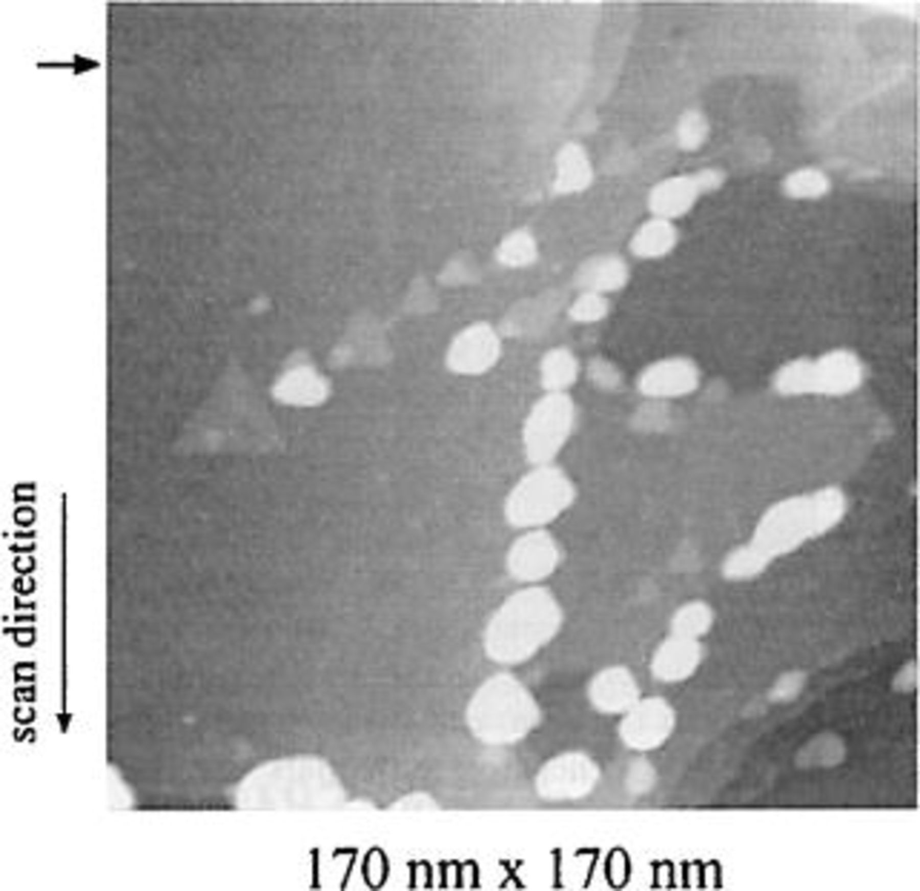
Figure 5. The invention of the scanning tunneling microscope in the 1980s has opened exciting new possibilities for the observation on an atomic scale of electrode surfaces and electrodeposition phenomena. The figure shows copper nuclei on a gold [111] surface obtained by electrodeposition from an acid sulfate solution by stepping the potential. The figure suggests that under the conditions of the experiment copper nuclei are formed exclusively at the monoatomic height steps on the substrate surface.52
To produce an image by STM or AFM the surface viewed must be scanned and this is a relatively slow process. For this reason the STM and AFM techniques are suitable only for studying relatively slow electrodeposition phenomena. In spite of this limitation, interesting information on step motion and surface diffusion has been obtained recently, by analyzing the fuzziness of growth steps in STM pictures.57 The STM can also serve as a tool for the local initiation of electrochemical phase formation. Local metal deposition can for example be initiated by producing a surface defect with the STM.58 In another method metal atoms are first deposited on an STM tip, then the tip is approached to the polarized substrate surface in order to initiate a transfer of atoms from the tip to the substrate surface. Using this technique arrays of well-defined copper or palladium clusters were produced.59 60 Similarly, cobalt clusters were produced by anodically dissolving the metal from an STM tip positioned close to the substrate.61
Several groups used the STM or the AFM to study the effect of additives on the formation and movement of atomic steps during the growth of electrodeposits. In an early study with copper it was found that benzotriazole (BTA) did not affect the nucleation, but inhibited growth of certain planes.62 The observed influence of BTA and thiourea on the growth morphology of copper deposits was attributed to their effect on surface diffusion.51 63 The role of substrate structure was also investigated and it was found that inhibiting additives adsorbed preferentially at defect sites.64 Most commercial plating electrolytes contain not one but several additives. For example, many copper plating solutions contain small quantities of chloride ion together with two or three organic additives having different functions.51 65 66 These additives act in conjunction through adsorption processes that inhibit or accelerate electrochemical reaction steps. A strong synergistic effect between polyethylene glycol and chloride ion was recently reported, copper deposition being inhibited only when both additives were present.66 Similarly, during pulse plating of copper-cobalt alloys it was found that a surfactant (SDS) added alone had a very different effect on the deposit morphology and the current efficiency than when it was added together with saccharin, a stress relieving agent.67 Different mechanisms by which additives may influence the electrochemical reactions at the electrode-solution interface have been discussed in a recent review from a chemical point of view.68 The author distinguishes blocking additives, complex-forming additives, ion pairing additives, surfactants and insoluble film forming additives. Acid-base concepts have also been considered.69 Using scanning probe techniques the evolution of deposit morphology in presence and absence of additives was studied with the aim to find scaling laws permitting to relate atomistic growth mechanisms to macroscopic models.51 63 70 Only a limited number of additives have been studied so far with scanning probe techniques and the different interaction mechanisms between additives are not yet well understood. As scanning probe and other sensitive in situ techniques become more widely used, one may expect that the scientific understanding of how synergistic and antagonistic effects of additives influence electrochemical phase formation will significantly improve. This could open the prospect of formulating plating electrolytes on a more rational basis in the future.
Electrochemical Engineering Aspects of Electrodeposition
Electrochemical engineering concerns the application of the principles of thermodynamics, kinetics, mass transport and current distribution to the scaling, optimization and control of electrochemical processes. Mastering these subjects has been crucial for the successful introduction of electrodeposition technology in electronics manufacturing. The theoretical foundations of current distribution and mass transport in electrochemical systems were laid in the 1940s and 1950s. Since then electrochemical engineering has developed into a recognized branch of electrochemistry71 and excellent textes describing the underlying principles are available.72 73 In the years covered by this report a large number of studies addressed problems of current distribution and mass transport in electrodeposition.
Current distribution is of critical importance for the design of plating cells and for the operation of industrial plating processes. It determines the thickness and uniformity of an electrodeposited coating and the shape evolution of the cathode in electroforming, leveling and superfilling. In alloy plating the distribution of the partial current densities on the cathode determines the uniformity of the chemical composition of the deposits. The current distribution prevailing on the cathode during an electrodeposition process is the result of several parameters such as cell geometry (primary current distribution), charge transfer kinetics (secondary current distribution) and mass transport conditions (tertiary current distribution). Numerical simulations involving all these effects are quite involved and require a detailed knowledge of prevailing hydrodynamic conditions. For this reason complete current distribution calculations have been performed for a limited number of electrochemical systems only, the rotating disk electrode being the classical example.74 For cell design purposes it is often sufficient to consider the limiting cases of primary current distribution or entirely mass transport controlled current distribution. Using these principles, a number of new designs for electroplating cells were developed in recent years. They include the rotating cylinder Hull cell,75 the uniform injection cell,76 the recessed rotating disk electrode77 and different types of jet cells with submersed or emerged electrolyte jets.78 79 80 81 The paddle cell82 83 developed for through mask plating of wafers on a laboratory or industrial scale offers a uniform current distribution over the entire surface. Mass transport conditions are fairly uniform although the mass transport rate may vary periodically with time as the paddle moves back and forth.84 Through hole plating poses difficult current distribution problems because the metal must be deposited uniformly into a high aspect ratio geometry. The current distribution in through hole plating using direct current85 86 and pulse current87 88 has been studied extensively. Another current distribution problem in electronics concerns the terminal effect that may occur when plating seed layers on an insulating substrate. In these applications the electrode resistance is not always negligible and potential gradients may develop in the cathode parallel to the metal-electrolyte interface. As a consequence, more material is plated in the vicinity of the electrical contact to the cathode than far from it. Dimensionless criteria have been proposed for estimating the importance of this effect.89
In through mask plating different scales must be taken into account with respect to current distribution and mass transport; the workpiece scale, the pattern scale and the feature scale.90 At the workpiece scale the primary current distribution depends essentially on the overall cell geometry. In some cases it can be improved by using auxiliary electrodes.91 On the pattern scale, the current distribution between the individual features forming the pattern depends strongly on their spacing and their geometry.92 93 Generally, the current density on a given feature tends to be higher when it is spaced farther away from a neighboring feature. The "active area density" which is the ratio between the area of the features and the geometrical area of the wafer has been found a useful concept for describing the current distribution on patterned surfaces.92 On the feature scale, the current distribution determines the shape of the growth front in through mask and in damascene plating and the shape of the dissolution front in electrochemical micromachining.90 94 95 96 Depending on experimental conditions, the current distribution on the feature scale is governed by the concentration field of the reacting species and/or by the potential field in the feature. Convection in cavities exposed to fluid flow has been theoretically modeled and it was shown that it can lead to asymetric concentration fields.97 98 In electroplating one controls the current distribution on the feature scale most often by using suitable additives.90
The effect of additives on the current distribution on microprofiles and the mechanism of cathodic leveling has been studied by a number of authors as early as the 1950s.97 98 The topic has found renewed interest in the 1990s because of its importance in electrochemical microfabrication and because numerical methods such as finite element and finite boundary element methods became available that facilitated quantitative modeling of shape changes. A quite unique feature of electroplating is that under certain conditions more metal is deposited into recesses than on protruding parts of a microprofile. This permits to achieve leveling of rough surfaces by cathodic metal deposition. The same behavior can be used to selectively fill small cavities on a patterned surface in Damascene plating (Fig. 6). It is generally accepted that leveling requires an inhibiting additive which is consumed at the cathode under mass transport control. Since recesses in a surface are less accessible than protrusions, metal deposition is less inhibited there and as a consequence the local deposition rate is higher than on the rest of the surface. Several groups have proposed quantitative models based on this concept.99 100 101 Leveling experiments with nickel using model profiles agreed well with theoretical predictions and confirmed that the rate of leveling depends on three dimensionless quantities, which characterize the ratio between mass transport and reaction rate of the additive, its reaction kinetics and its adsorption properties.102 The shape evolution during electrodeposition of copper bumps has been studied both theoretically and experimentally.103 104 The Peclet number and the resist angle were found to be the most critical quantities determining the resulting shape. Superfilling in Damascene plating has been modeled assuming that the additive reacts under diffusion control and that the metal deposition is activation controlled.90 105 By optimizing the reaction conditions in presence of additives it was possible to achieve a flat growth front in the features. More recently, a different model for superfilling of narrow deep cavities was proposed, which includes not only inhibition but also an accelerating effect of additives, the extent of which was assumed to depend on curvature.106 107
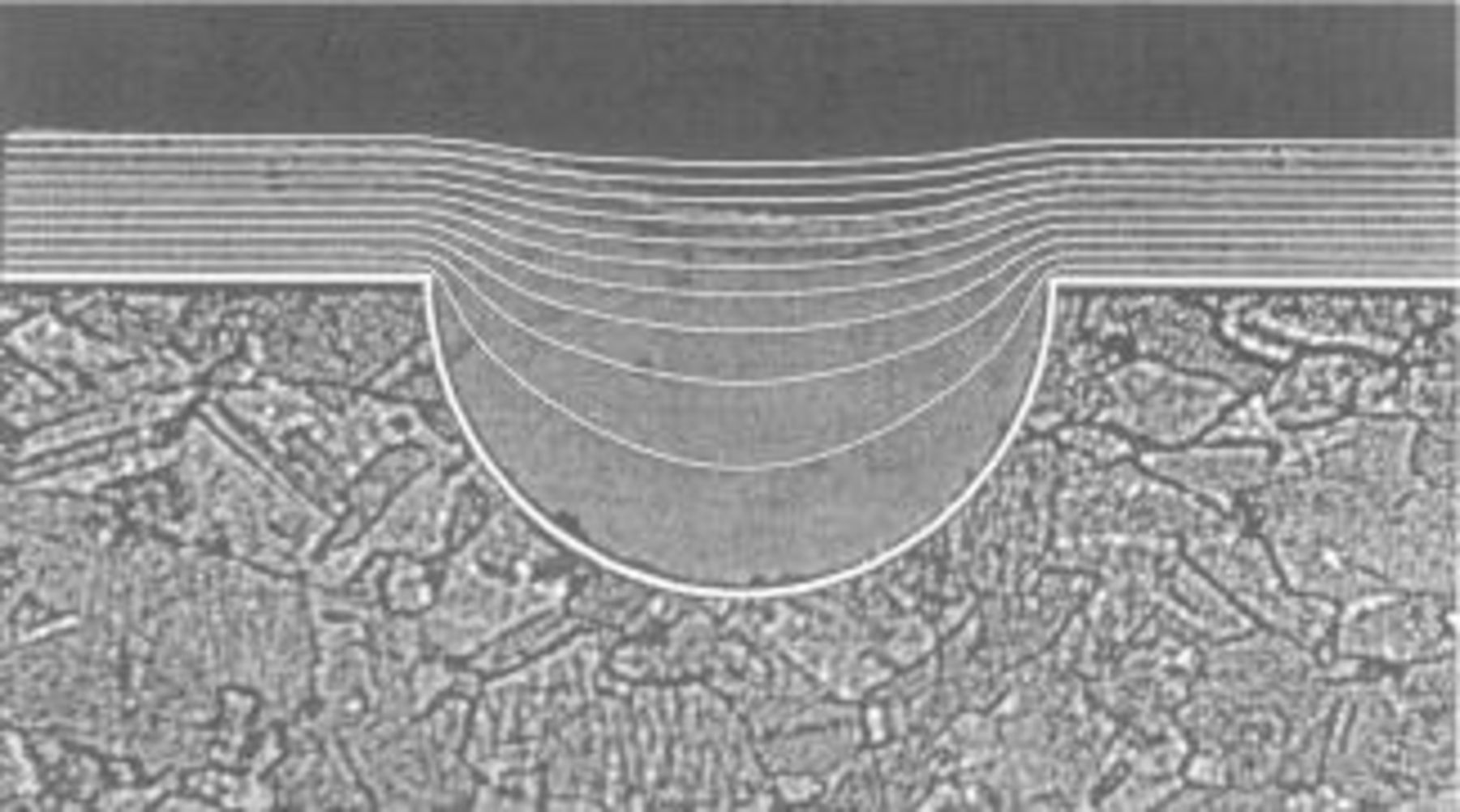
Figure 6. Electrodeposition is unique in that it permits under certain conditions to preferentially deposit material into recesses of a surface. The behavior is used to achieve leveling in plating of coatings and superfilling in damascene plating. The figure illustrates filling of a hemispherical groove by electrodeposition of nickel in presence of a leveling agent. A cross section of the actual deposit is shown together with numerical simulations of the shape change for increasing amounts of charge passed. The calculation takes into account mass transport and adsorption of the leveling agent.102
The use of pulse current or pulse reverse current provides an elegant way to influence the current distribution in electrodeposition.108 In the absence of significant mass transport effects, the current distribution in pulse plating is less uniform than in dc plating because of the lower Wagner number. On the other hand, plating under conditions where nonsteady state mass transport controls the rate of deposition can lead to a more uniform current distribution compared to dc plating.109 Using a rotating disk electrode it was shown that with pulse reverse current a more homogenous current distribution can be achieved than with simple pulse current, because conditions can be chosen such that during the anodic cycle the metal dissolves preferentially from the outer part of the disk.110 By the same mechanism, pulse-reverse current was found to be a viable method for improving the deposit uniformity in through hole plating.86 111
Electrodeposited Materials
Structure and properties of electrodeposits
Materials science deals with the relationships between processing, structure and properties of materials. Materials science aspects of electrodeposition have been the subject of several recent ECS symposia.112 113 114 Indeed, a wide range of metals and alloys with different structure and composition can be electrodeposited. Electrodeposition normally takes place far from equilibrium, and therefore microstructures and alloy compositions can be achieved that are not accessible by conventional metallurgical means (Fig. 7). For example, X-ray amorphous alloys115 116 117 or nanocrystalline metals and alloys118 119 120 have been obtained by electrodeposition. Another particularity of electrodeposition is that small changes in process conditions, for example the presence or not of tiny amounts of additives or of complexing agents, can have enormous consequences for the resulting microstructure and composition of the deposited materials and hence for their properties. If not controlled, this behavior can lead to reproducibility problems in laboratory experiments and in production. Careful monitoring of electrolyte composition therefore is a critical factor for success in industrial electrodeposition.121 On the other hand, if processing conditions are rigorously controlled electrodeposition offers the possibility to fabricate materials with tailor made structure and properties.113 Frequently, internal stress develops in electrodeposits. Several factors may contribute to this, such as mismatch between substrate and deposit, grain coalescence during growth and incorporation of electrolyte species or of hydrogen.122 123 124 125 Internal stress can cause cracking of deposits or loss of adhesion. A good review of different methods for measuring stress in electrodeposits has been published in the early 1970s.126 Several more recent papers discuss methods for in situ measurement of internal stress during electrodeposition including X-ray diffraction,127 128 bending of thin film substrates,129 130 strain gauge,131 and the use of the electrochemical quartz crystal microbalance.132
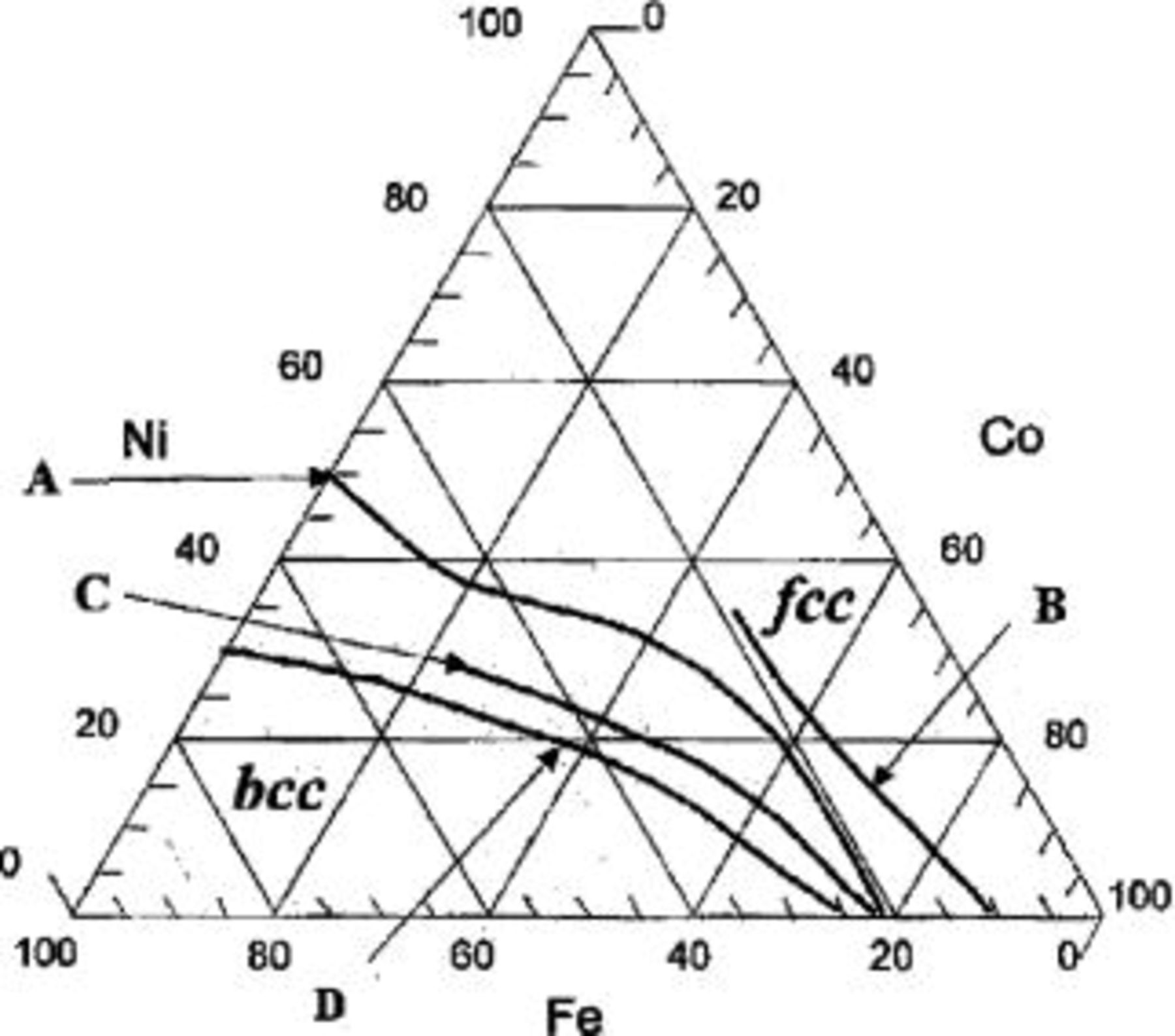
Figure 7. Most electrodeposition processes take place far from equilibrium and for this reason materials not readily obtained by classical metallurgical methods can be made including nanocrystalline and amorphous materials. Generally, the structure and properties of electrodeposited metals and alloys vary strongly with the deposition conditions. The figure shows in a ternary diagram the fcc-bcc phase boundaries of CoNiFe alloys electrodeposited from solutions containing different additives, namely (A) saccharine, (B) thiourea, (C) a nonsulfur containing compound. The data show that the phase boundary and therefore the magnetic properties of the alloys are strongly affected by the nature of the additive.21
Copper is probably the most widely studied metal in electrodeposition, because of its industrial importance and because its noble equilibrium potential makes it well suited for fundamental studies without interference of hydrogen formation. The 1990s saw an enormous increase in the number of studies on copper electrodeposition stimulated by its use in electronics packaging. Much knowledge therefore is available on the mechanism of copper deposition and how deposition conditions affect deposit structure and properties. A survey of early work on the electrocrystallization of copper can be found in Ref. 133. Most of the research in the 1960s focussed on the study of interfacial kinetics and transient phenomena. An important result was the establishment of the reaction mechanism of the copper electrode.134 Copper deposition and dissolution in sulfate solution was shown to involve two consecutive charge transfer steps, the copper(I)-copper(II) step being rate-limiting. More recent studies deal with the interactions of additives with the monovalent copper intermediate.135 136 The role of inhibition and of applied current density on deposit morphology has been studied extensively. Increasing inhibition and/or increasing current density was found to favor formation of fine grained deposits. The microstructures observed with copper have been summarized in a schematic diagram having as its y-axis the degree of inhibition and as the x-axis the applied current density divided by the copper ion concentration.133 137 It has been known for some time that electrodeposition under limiting current conditions leads to dendritic or powdery deposits.138 Therefore, the value of applied current density with respect to the mass transport limited current density is a critical parameter for deposit morphology. Similarly, the degree of inhibition can be expressed as the ratio of applied current density to exchange current density.139 140 Several papers discuss various aspects of the relationship between deposit microstructure and electrochemical conditions for deposition of copper and other metals.43 122 139 140 141 Quite generally, kinetically limited growth tends to favor compact columnar or equiaxed copper deposits while mass transport limited growth favors formation of loose dendritic deposits.
Additives, typically small amounts of chloride in conjunction with two to three organic compounds, are widely used in industrial copper plating from acid sulfate solutions.51 101 The additives are not only needed for leveling and superfilling, but they also affect the structure and roughness of the deposits. Inhibiting additives tend to promote the formation of small equiaxed grains142 which may lead to increased internal stress. Many additives are incorporated into the deposit.143 The incorporation of additives was found to change the microstructure of copper deposits and to lower their electrical conductivity.144 Copper deposition from sulfate solutions can lead to the formation of nonequilibrium grain structures, which spontaneously recristallize even at room temperature. As a consequence, structure dependent materials properties such as electrical conductivity or internal stress may change slowly with time after deposition.145
Pulse plating is an interesting method for controlling the microstructure of electrodeposits.146 Early studies on copper, gold and cadmium suggested that pulse plating leads to refinement of the grain structure of copper, which was attributed to the high instantaneous current densities favoring nucleation.147 A later study of the effect of pulse current parameters on the microstructure of copper deposited from sulfate electrolytes indicated that nonsteady state and steady state mass transport conditions are the most crucial parameters.148 Well below the pulse limiting current and the steady state limiting current the deposit structure was not affected by the applied pulse parameters, because copper atoms were apparently added at step and kink sites rather than forming 3D nuclei. Several studies found that for nickel deposition the use of pulse plating leads to deposits of finer grain size119 120 149 and increases their hardness and their corrosion resistance.120 149 In another study, pulse plating was found to affect the crystal structure of chromium deposits because of different hydrogen charging.150 It would appear from the mentioned literature that the deposit structure in pulse plating depends on the nucleation mechanism and adsorption phenomena as well as on mass transport conditions, but a general theory in this field is still lacking.
Fundamentals of alloy deposition
A comprehensive compilation of electrolytes and electrochemical conditions for alloy deposition has been published in the early 1960s.151 Most of the practical information given therein remains of interest today. More recent overviews on electrodeposition of different metals and alloys are found in the fourth edition of Modern Electroplating published under the auspices of ECS.8 Reviews covering fundamental aspects of alloy deposition152 153 or electrodeposition of functional alloys for magnetic applications16 20 are also available. During the last thirty years research on alloy deposition was stimulated greatly by the needs of the electronics industry for functional alloys and by the search for new coatings for corrosion protection. The availability of new tools and methods for electrochemical experimentation, materials characterization and theoretical simulation provided a further stimulus. From a fundamental point of view, alloy deposition can be understood by considering the thermodynamics and kinetics of the partial electrode reactions in a system involving multiple reactions.153 Often, the partial electrode reactions do not proceed independently but are coupled through adsorption processes or solution equilibria. The quantitative investigation of codeposition phenomena therefore usually requires numerical modeling. The mechanism of so called anomalous codeposition, has been extensively studied, because of the industrial importance of iron group alloys for magnetic heads and of zinc alloys for corrosion protection. In anomalous codeposition a higher proportion of the less noble metal is found in the deposit than in the solution,151 a behavior typically observed with iron group metals and with zinc. Different groups studied the anomalous codeposition of Fe-Ni alloys and proposed models for explaining the codeposition mechanism and for predicting alloy composition as a function of different variables such as potential or convection conditions.154 155 156 157 158 159 160 Originally, the anomalous effect was attributed to the formation of an oxide-hydroxide layer at the cathode surface.154 A later model considered mostly the effect of solution equilibria in the cathodic diffusion layer.155 More recent papers explained anomalous codeposition of Fe-Ni alloys by the competitive adsorption of reaction intermediates, which leads to inhibition of nickel deposition.156 160 Of late, it was observed that in addition the codepositing nickel enhances the rate of codeposition of iron158 159 and a theoretical model was proposed that takes into account both inhibiting and accelerating effects.157
Certain metals like tungsten or molybdenum, which cannot be deposited from an aqueous solution, readily codeposit with iron group metals forming an alloy. The phenomenon known as induced codeposition151 has recently been theoretically modeled by postulating a mechanism that involves an adsorbed mixed reaction intermediate of the codepositing metals.161 Alloy formation during codeposition of small amounts of Pb and Sn with copper162 as well as of Ni with Al in a molten salt electrolyte163 has been attributed to underpotential deposition. Since no underpotential deposition of molybdenum on iron group metals has been observed such a mechanism can not explain induced codeposition of these metals. Quite generally, significant progress in the theoretical understanding of alloy deposition has been achieved in recent years thanks to theoretical modeling based on numerical simulation. Theoretical models for codeposition typically take into account mass transport and chemical equilibria, competitive adsorption and charge transfer kinetics. They permit to simulate how experimental parameters such as applied potential or convection conditions affect the composition of electrodeposited alloys and many such predictions were successfully tested by experiment. However, most alloy deposition models proposed in the literature require knowledge of rate constants derived from codeposition experiments under similar conditions and in addition they usually involve assumptions as to the nature of adsorbed species.157 At this time, codeposition phenomena involving coupled partial reactions cannot be quantitatively predicted from the electrochemical properties of the participating metals alone.
Pulse plating provides additional means to influence composition and structure of electroplated alloys.146 153 164 165 166 In the 1980s and 1990s several groups used numerical modeling for the study of pulse plating of alloys.167 168 169 170 171 These models usually consider steady state and nonsteady state mass transport as well as interfacial kinetics. It has been found that displacement reactions during the off time can have an important effect on resulting alloy composition.171 Theoretical models were proposed which take into account this effect and they were successfully tested with copper-nickel and copper-cobalt alloys.172
Alloys for magnetic applications
Electroplated alloys are widely used in magnetic read and write heads. Several Proceedings of ECS symposia provide evidence for the impressive progress achieved in regard to processing technology and properties of electrodeposited magnetic alloys.112 173 A recent review presents a detailed discussion of materials requirements and deposition conditions of promising alloys.16 Magnetic writing requires magnetically soft materials with high saturation magnetization, low coercivity and low magnetostriction.174 Originally, permalloy was used, which is a Ni-Fe alloy containing 19 % Fe with a saturation magnetization of about 1 Tesla. Much research over the years was carried out to develop alloys with higher saturation magnetization. Increasing the Fe content of Ni-Fe alloy or replacing nickel by cobalt can be used towards this end. Still higher values of saturation magnetization are achieved with electroplated ternary alloys.16 The magnetic properties of electrodeposited CoNiFe alloys were found to depend on their composition and microstructure.21 Among other, they are modified by the presence of sulfur containing additives such as saccharin or thiourea.175 The line separating the bcc and fcc phases in the ternary diagram Fe-Ni-Co is shifted depending on the additive used. Sulfur containing additives lead to incorporation of sulfur into the deposit. While this permits to influence phase formation and grain size, it may negatively affect the corrosion properties.176 By careful optimization of deposition parameters nanocrystalline ternary alloys with a grain size on the order of 10 nm were produced that exhibited saturation values of 2 Tesla or more.21
Multilayer alloys have been an important field of research during the last 20 years. The first electrodeposited multilayer alloy films (also referred to as composition modulated alloys or CMA in the literature) were reported in 1983.177 By periodically varying the potential, well-defined Ag-Pd multilayers could be produced from an electrolyte containing both silver and palladium salts. The films were intended for electrical contacts having a good corrosion resistance and good electrical conductivity. The same technique was applied in the mid 1980s to the deposition of Ni-Cu multilayer alloys178 to study their mechanical properties. Decreasing the layer thickness to below 0.4 micrometer resulted in a strong increase in tensile strength. A few years later the potential interest of Cu-Ni and Co-Ni multilayer alloys for magnetic applications was discovered.179 This led to a considerable number of studies on structure and properties of multilayer alloys and to the investigation of how the structure and spacing of the layers influence the magnetic properties, especially the magnitude of the giant magnetoresistance (GMR) effect (Fig. 8). A comprehensive review of the literature on electrodeposited magnetic multilayer alloys was published in 1996.180 The same potential modulation technique used for fabricating multilayer alloys can also be applied to fabricate composition modulated nanowires using a porous polymer membrane or a porous aluminum oxide as a template.181 Three-dimensional nanostructuring of pulse plated Cu-Co multilayers was recently achieved due to columnar growth of copper rich and cobalt rich phases.182
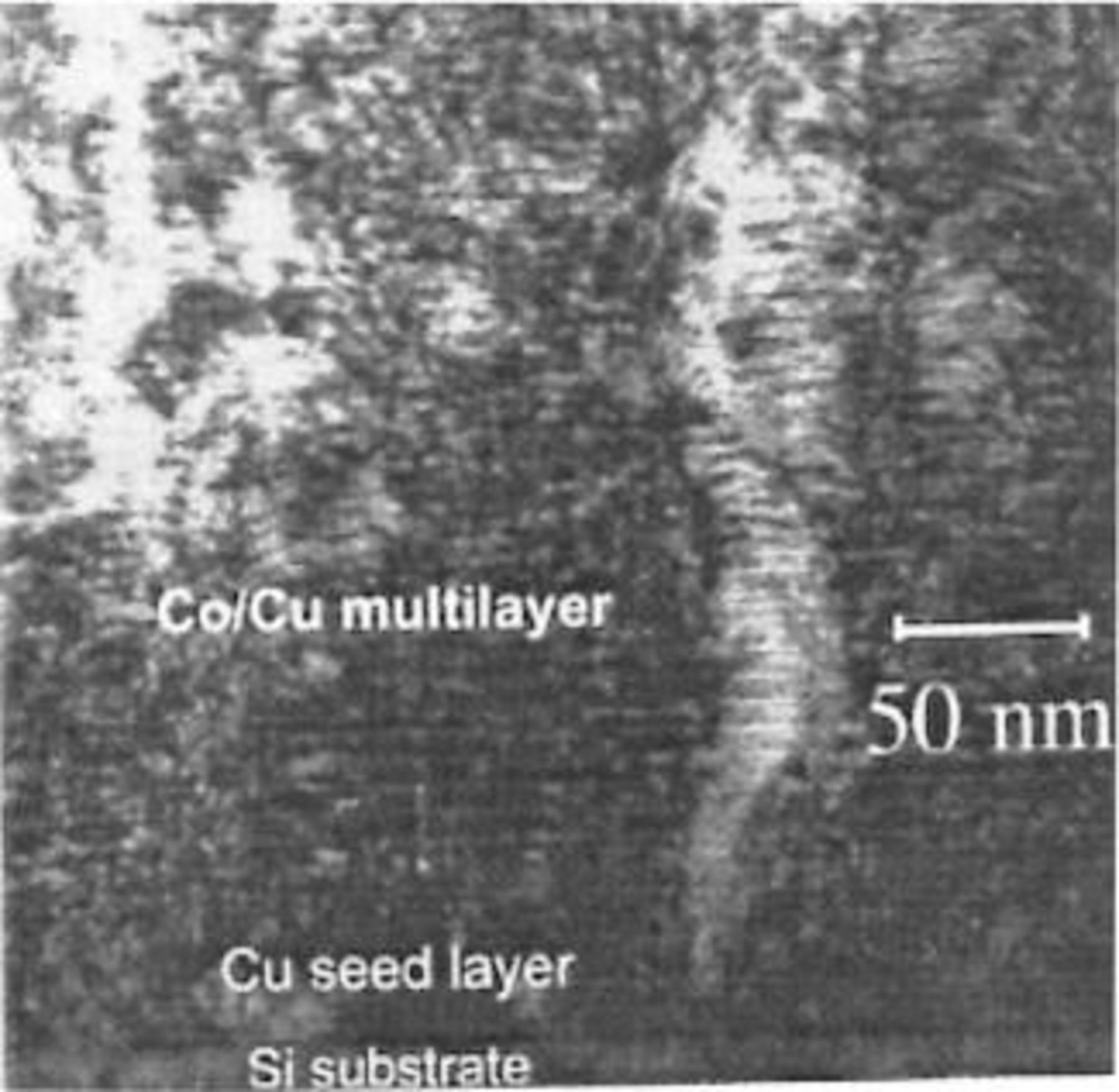
Figure 8. Multilayer alloys with alternating layers of magnetic and a nonmagnetic materials, each layer just a few nanometer thick, exhibit the so-called giant magnetoresistance effect, meaning that their resistance changes markedly when a magnetic field is applied. These materials are used in a new generation of magnetic heads for high density magnetic storage. Multilayer alloys can be electrodeposited from a suitable electrolyte by periodically varying the current or the potential. The figure shows a TEM micrograph of a nano-modulated Co-Cu multilayer alloy electrodeposited on a silicon [110] substrate. The deposits exhibit columnar growth mode as confirmed by electron diffraction.229
Materials for corrosion and wear protection
Electrodeposited and electroless coatings find a wide range of industrial applications for corrosion and wear protection. In particular, zinc and Zn-Ni alloy coatings with about 15 to 20% Ni are extensively used in the automobile industry for corrosion protection of steel. Codeposition of zinc with iron group metals involves anomalous codeposition, the deposition of the iron group element being inhibited by the codepositing zinc in chloride as well as sulfate electrolytes.152 183 A number of papers deal with the mechanism of electrodeposition of Zn-Ni alloys and different sometimes contradictory models have been proposed.184 185 186 187 In one paper impedance data are interpreted in terms of a mixed adsorbed reaction intermediate.184 Another study found that the polarization curve for deposition of Zn-Ni alloys exhibits an inversion before the onset of anomalous codeposition. To account for this behavior and for observed impedance data a reaction model with twenty-five parameters was developed.185 A different theoretical model considering transport by convective diffusion and migration at a rotating disk electrode attributed the anomalous codeposition behavior to an increased exchange current density of Zn.186 Codeposition of hydrogen was thought to enhance nickel deposition during the first stages of Zn-Ni alloy formation which apparently involved discrete nuclei of zinc and nickel.187 The phase structure of electrodeposited zinc alloy coatings differs from that of thermally produced alloys and it strongly depends on deposition conditions.188 Similarly, the phase structure and composition of pulse plated Zn-Ni alloys varies with the applied pulse parameters.165 Generally, the corrosion resistance of Zn-Ni alloy coatings is superior to that of zinc metal coatings, permitting to apply a smaller coating thickness.5 184 Electroplated Zn-Fe alloys are less corrosion resistant than Zn-Ni alloys unless they are subjected to a chromate treatment.189
Electroplated and electroless composite materials can be fabricated by codeposition of a metal and a powder suspended in the electrolyte. Ni/SiC composite coatings obtained by electrochemical codeposition of SiC powders with nickel are used for cylinder linings in the automobile industry.12 During the 1970s electroless Ni-P/SiC composite alloy coatings were developed for various tribological applications. Generally, the incorporation of hard particles such as carbides, oxides, borides or diamond leads to dispersion hardening and thus permits to improve wear resistance of the matrix material.190 The mechanism of codeposition has been studied by a number of groups and theoretical models of varying degree of complexity and sophistication have been proposed.191
192 It is generally agreed that codeposition of SiC involves transport processes193 and adsorption.194
195 However, many phenomena associated with particle codeposition are not yet well understood. For certain tribological applications such as self-lubricating bearings, it is advantageous to incorporate soft rather than hard particles into metal deposits. The soft particles act as solid lubricants that reduce friction. Electroless or electrodeposited metal matrix composite coatings containing  196 or PTFE13
197 exhibit selflubricationg properties. Electroless Ni-P/PTFE coatings are well established in industry. Interestingly, they exhibit satisfactory friction and wear behavior only under oxidizing conditions, which permit the formation of a passive oxide film on the surface.198 Recently, nontribological properties of electrodeposited composite coatings have become of interest. Among other, the catalytic properties and electrochromism of electroplated metal-oxide and similar materials have been studied199 and the suitability of electrodeposited Ni/PTFE coatings as hydrophobic electrodes for organic reduction and oxidation reactions has been explored.200 Nontribological applications of electrodeposited composite coatings could well become more important in the future.199
196 or PTFE13
197 exhibit selflubricationg properties. Electroless Ni-P/PTFE coatings are well established in industry. Interestingly, they exhibit satisfactory friction and wear behavior only under oxidizing conditions, which permit the formation of a passive oxide film on the surface.198 Recently, nontribological properties of electrodeposited composite coatings have become of interest. Among other, the catalytic properties and electrochromism of electroplated metal-oxide and similar materials have been studied199 and the suitability of electrodeposited Ni/PTFE coatings as hydrophobic electrodes for organic reduction and oxidation reactions has been explored.200 Nontribological applications of electrodeposited composite coatings could well become more important in the future.199
Electrodeposited semiconductor materials
Electrodeposition of chalcogenide semiconductor compounds from aqueous solution is a potentially simple and cheap process. An inherent problem, however, is the comparatively low purity of electrodeposited semiconductors compared to those produced by vapor phase deposition, especially molecular beam epitaxy. The most promising application of electrodeposited semiconductor compounds is thought to be in large area solar cells where economy of scale is more important than uttermost control of purity. Electrodeposition of CdTe was reported in 1978 and theoretical aspects of codeposition leading to compound formation were discussed.201 Since then a number of different selenides, sulfides and tellurides have been electrodeposited such as ZnSe, CdSe, PbSe, CuSe,  ZnS, CdS, ZnTe, and mixed compounds such as Cd(Hg)Te, (CdZn)S,
  and
and  202 The deposition mechanism of CdTe is typical for the cathodic reactions leading to semiconductor compound formation by electrodeposition. Reduction is thought to proceed in two steps. In a first step the tellurium is formed by reduction of telluric acid. In a second step the Cd undergoes underpotential deposition on tellurium sites on the surface.202 A similar mechanism apparently applies to electrodeposition of zinc oxide in presence of oxygen or hydrogen peroxide.203 The electrodeposition mechanism of ternary compounds such as
  involves several reaction steps, but the deposit composition depends to a large extent on the relative magnitude of the diffusion fluxes of the codepositing species.204
205 Electrodeposition has also been used to produce epitaxial deposits of semiconductors. The technique involves the use of two electrolytes, which are alternatively admitted to the deposition cell.206
207 The potential of the cathode is chosen such that alternatively each element of the compound semiconductor undergoes a UPD reaction forming a single atomic layer. At the time of this writing the practical applicability of this procedure for device fabrication appears to be limited, however.
involves several reaction steps, but the deposit composition depends to a large extent on the relative magnitude of the diffusion fluxes of the codepositing species.204
205 Electrodeposition has also been used to produce epitaxial deposits of semiconductors. The technique involves the use of two electrolytes, which are alternatively admitted to the deposition cell.206
207 The potential of the cathode is chosen such that alternatively each element of the compound semiconductor undergoes a UPD reaction forming a single atomic layer. At the time of this writing the practical applicability of this procedure for device fabrication appears to be limited, however.
Related Electrochemical Processes
The interests of the Electrodeposition Division of ECS include not only electrodeposition and its different applications but also related processes such as electroless plating (Fig. 9) and anodic dissolution applied to electropolishing, electrochemical machining and electrochemical etching. To keep this review within a reasonable length these processes will be mentioned only briefly and the reader is referred to the indicated literature for more information. Electroless plating uses chemical reducing agents such as hypophosphite or formaldehyde as a source of electrons in place of a cathodic current. The process, which can be considered a corrosion process in reverse, is best described by mixed potential theory.208 Recent overviews of the theory and applications of electroless plating are given in Ref. 209 and 210. Electroless plating of nickel-phosphorous alloys is widely used to produce coatings for corrosion and wear protection. More recently, electroless plating has found many new applications in electronics manufacturing, especially for packaging and for producing diffusion barriers.211 212 Electroless plating requires a more elaborate bath control than electroplating, but on the other hand, it provides better throwing power and it does not require conducting substrates.
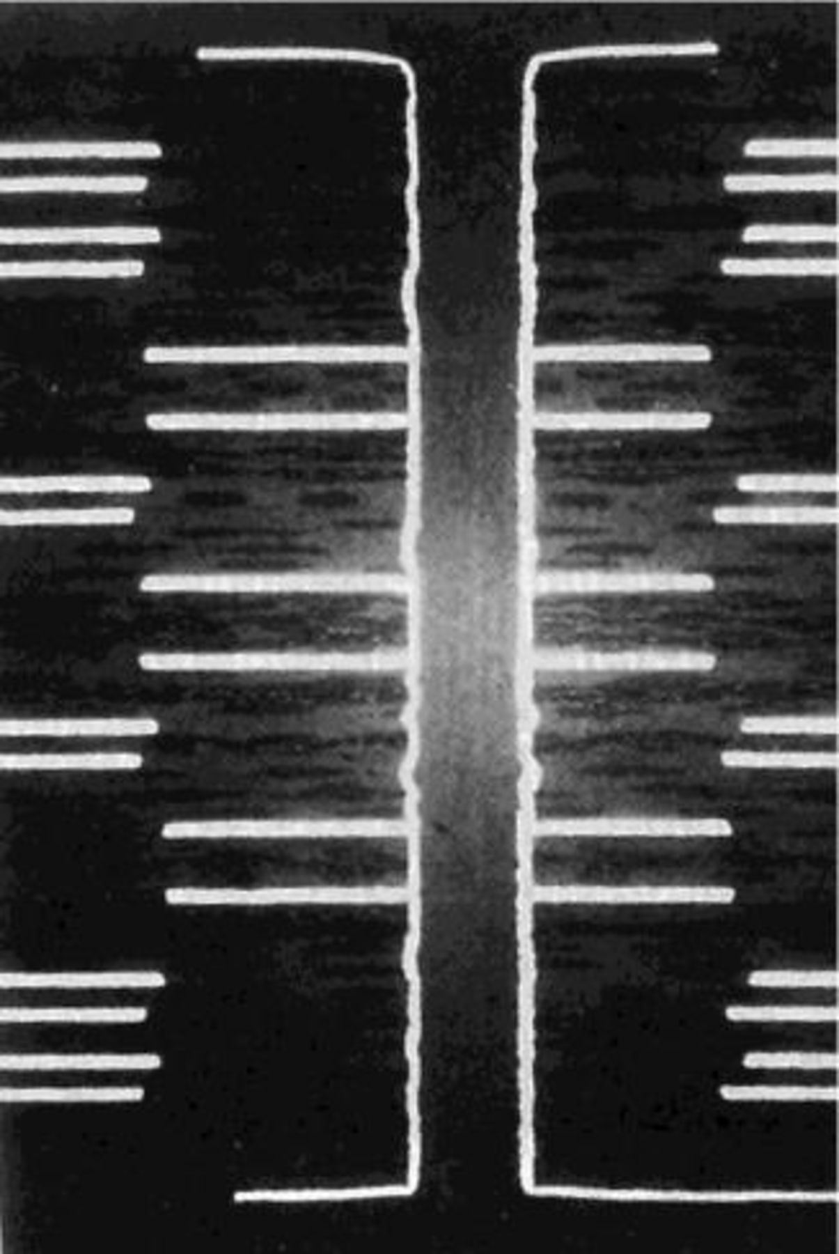
Figure 9. In electroless plating a reducing agent supplies the electrons for reduction of metal ions. The process exhibits a high throwing power and it can also be used for plating on insulators. Electroless nickel-phosphorous alloys and nickel-phosphorous composite materials containing hard or soft phases are widely used for corrosion and wear protection. In recent years, electroless plating has become an important technology in the electronics industry. The figure shows the cross section of a circuit board with a high aspect ratio through-hole plated with electroless copper. The thickness of the board is 4 mm, the hole diameter 0.25 mm] corresponding to an aspect ratio of 16. The figure demonstrates the excellent uniformity of the deposit thickness over the entire length of the through hole.210
Electropolishing finds numerous applications in the manufacturing industry for polishing of metallic objects of complex shape. Fundamental aspects of the process have been reviewed covering the literature up to 1987.213 More recent studies of electropolishing are found in Ref. 214 215 216 217 218 219. Electrochemical machining (ECM) was developed in the 1960s for machining of complex shapes in hard to machine alloys used mostly by the aerospace industry.220 Current densities applied in ECM are two to three orders of magnitude higher than in electrodeposition and therefore the process requires intense electrolyte flow for evacuating reaction products and heat generated in the inter electrode gap. For most metals and alloys anodic dissolution under these conditions takes place in the transpassive potential region.221 During the 1980s and 1990s electric discharge machining has taken over many tasks of ECM, because it is easier to control and does not need elaborate electrolyte pumping and filtering installations. On the other hand, during this period electrochemical micromachining (EMM) has emerged as a new manufacturing technology for micromechanics and electronics.3 222 223 224 225 226 227 EMM is based on controlled anodic dissolution through masks. The process does not require heavy installations and permits precision fabrication of microstructures using well established photolithographic techniques. Recently, a mask free electrochemical micromachining process has been described, which uses laser irradiation for forming a pattern on an anodically grown oxide film that acts as a mask during anodic dissolution.228
Concluding Remarks
This review describes significant developments in electrodeposition science and technology that took place during the last part of the twentieth century. Electrodeposition has become a broad field with many ramifications making it extremely difficult for a single person to be aware of all important developments. The selection of topics and references in this review therefore necessarily contains some subjectivity, reflecting the authors own experience and limitations. Readers are kindly asked to forgive unavoidable shortcomings and omissions. According to W. Blum,1 "a historian must in some degree also be a prophet." Keeping in mind the popular wisdom "predictions are always difficult, especially when they concern the future" let us therefore conclude this review with a short glance at what could be future trends and developments.
Sustained environmental pressures, emerging nanotechnology and the need for tailor made functional materials for microsystems will be strong driving forces for future research, innovation and process development in the field of electrodeposition and related processes. The economic importance of electrochemical microfabrication technology will likely continue to grow in the coming years, including not only electrodeposition but also electroless deposition and electrochemical micromachining. Continuing miniaturization in information technology and the emerging nanotechnology, will lead to an increasing need for understanding the kinetics of electrochemical phase formation and electrochemical reaction mechanisms on an atomic scale. This will further increase the importance of in situ experimental methods capable of providing information on phenomena at solid-liquid interfaces on a nanometer scale, including powerful physical and spectroscopic methods and new types of scanning probe techniques. Such research should eventually lead to a better understanding and control of electrodeposition processes with and without additives, and it may offer new opportunities to electrodeposit not only metals and alloys, but also nonmetallic materials such as compound semiconductors or functional oxides on a variety of substrates. The importance of numerical modeling will further increase, including ever more realistic assumptions concerning chemical and physical mechanisms involved in metal and alloy deposition and an ever wider range of length scales. This should eventually permit to link atomic scale phenomena with macroscopic process models and materials properties. Powerful and user friendly software for simulating metal and alloy deposition kinetics will increasingly become available. As a consequence the plating industry will be in a position to routinely apply numerical modeling for electrolyte development and process optimization. This should facilitate the development of new environment friendly processes and functional materials for specific applications.
During the last part of the twentieth century, electrodeposition science and technology contributed significantly to the emergence of our modern information society. There are many reasons to believe that in the twenty first century electrodeposition and related technologies will have an equally important or even more important impact. The Electrochemical Society through its symposia and publications has contributed to the development of electrodeposition science and technology in the past and it is expected that it will continue to stimulate advancements in the field also in the future.