
Abstract
The physical bulk properties of metalorganic chemical vapor deposited (MOCVD) deposited  layers were characterized as a function of deposition temperature, thickness, and starting surface. It is shown that depositing
  layers at 300°C results in a lower density film compared to films deposited at higher temperature (e.g., 485 and 600°C). In addition, it is shown that layers deposited at 300°C contain significant amounts of carbon originating from the organic precursor (tetrakis-diethylamidohafnium). As a result of the low density and/or carbon contamination, the dielectric properties of these layers are very poor. It is observed that the density of the film is heavily dependent on the thickness, where very thin layers have a density that is only a fraction of the bulk density regardless of the deposition temperature. For thicker layers, a higher deposition temperature is seen to result in a higher density, although still lower than bulk density, as observed by ellipsometric porosimetry. Finally, the crystalline state of the material is found to be dependent on the deposition temperature, thickness, and post-deposition anneal. Based on our results, MOCVD deposited
  layers are expected to be polycrystalline and present in its cubic and/or monoclinic phase. © 2004 The Electrochemical Society. All rights reserved.
Export citation and abstract BibTeX RIS
The aggressive scaling of complementary metal oxide semiconductor (CMOS) devices is driven by the desire for enhanced performance, higher integration levels for increased functionality, and the reduction in cost per function and per speed.1 Scaling the transistor requires making the gate dielectric thinner as well.  has been the industry choice as the gate dielectric for its excellent properties such as a high-energy bandgap, its high-quality growth on Si, it remains amorphous up to very high temperatures, and its interface states can easily be passivated. However, the scaling limit of
  as the gate dielectric has been reached due to the unacceptably high leakage current associated with quantum mechanical tunneling. As a result, new materials are being explored that can serve as the replacement for
  These new materials have a higher dielectric constant, typically on the order of 20 to 30 (high k materials) allowing for a thicker gate dielectric to drastically reduce the gate leakage current, while increasing the gate capacitance resulting in improved performance.2 Several candidates are being screened and the results clearly demonstrate the complexity of integrating these materials into existing CMOS process flows. High k stability with silicon is a major issue recurrently reported in literature, examples include the Si in-diffusion for
 and
and  3
4
5 resulting in silicate formation, silicide formation for
3
4
5 resulting in silicate formation, silicide formation for  6
7 and in most cases the formation of an interfacial layer between the Si substrate and the high k layer during deposition and/or after post-deposition treatments.8
9
10 At present, the industry is mainly focusing on Hf-based materials to replace
6
7 and in most cases the formation of an interfacial layer between the Si substrate and the high k layer during deposition and/or after post-deposition treatments.8
9
10 At present, the industry is mainly focusing on Hf-based materials to replace  e.g.,
e.g.,  Hf-aluminates, and Hf-silicates.
In this paper, we focus on the growth behavior and various physical properties of the bulk  material including the crystallization behavior, organic contamination, and especially the layer density as a function of thickness and deposition temperature. Analysis techniques included spectroscopic ellipsometry (SE), time of flight secondary-ion mass spectroscopy (TOFSIMS), Rutherford backscattering spectroscopy (RBS), X-ray diffraction (XRD), thermal desorption spectroscopy (TDS), ellipsometric porosimetry (EP), atomic force microscopy (AFM), and transmission electron microscopy (TEM).
Experimental
 layers were deposited by metalorganic chemical vapor deposition (MOCVD) at temperatures ranging from 300 to 600°C and with varying thickness. We have used the organic precursor (tetrakis-diethylamidohafnium (TDEAH)) and
  to deposit these layers on 8 in. Si (100) wafers in an Applied Materials MOCVD-chamber based on the Tanox chamber. The layers are deposited at a pressure of 4 Torr, with
  and
and  flow rates of 1.5 and 1 slm, respectively. The Hf flow equals 6 mg/min in 0.65 slm
  -carrier gas. The starting surfaces included hydrogen-passivated Si, chemical oxides (IMEC-clean:
  -Marangoni dry),11 and oxides grown by rapid thermal oxidation. In another paper, we report on the formation of an interfacial layer in between the
  and the Si substrate during the MOCVD process independent of starting surface.12 The main conclusion is that the MOCVD process results in a Hf-silicate interfacial layer approximately 1 nm thick.
Thickness measurements were done using a KLA-TENCOR ASET F5 spectroscopic ellipsometer. The ellipsometer recipe used for the thickness measurements determines both refractive index and thickness minimizing the effect of compositional changes on the film thickness. We found there to be a good correlation between the thickness as determined with ellipsometry and TEM. TOFSIMS profiles were measured with an IONTOF IV instrument in the dual beam configuration. The positive ion profiles were measured in the Ar (10 keV)-Ar (500 eV) configuration and the negative ion profiles were measured in the Ga (15 keV)-Xe (500 eV) configuration. TDS measurements were performed under nitrogen at atmospheric pressure while the desorbed gasses were analyzed by means of an atmospheric pressure ion mass spectrometer (APIMS-VG Instruments Trace+). The samples were heated from room temperature to 900°C at an average rate of 1°C/s in an RTP chamber (Steag-AST SHS 2800).13
14 TEM analysis was performed with a Jeol 200CX electron microscope operating at 200 kV. The cross-sectional specimens were prepared by conventional ion milling. Open-circuit potential (OCP) was measured in situ during wet etching of the dielectric layer on a silicon surface, as a function of time, relative to a reference electrode (Ag/AgCl).15 Wafer pieces of 4 × 4 cm served as the working electrode. Both reference and silicon substrate electrodes were connected through a mV meter in a 0.5%  solution. A more theoretical background of OCP analysis can be found elsewhere.15
16
17
solution. A more theoretical background of OCP analysis can be found elsewhere.15
16
17
Results and Discussion
Growth kinetics and density.—
The growth kinetics of MOCVD deposited  layers were investigated by constructing growth curves for three different deposition temperatures (300, 485, and 600°C) on a 1 nm
  starting surface (grown by rapid thermal oxidation (RTO)). A plot of the total film thickness (interfacial
  vs. the deposition time exhibits a linear relationship (Fig. 1). The deposition rate, expressed as nm/s, is comparable for deposition temperatures of 485 or 600°C, but distinctly higher for deposition at 300°C. This suggests that the deposition rate depends upon the deposition temperature.

Figure 1. Thickness as a function of the deposition time for  films deposited on a 1 nm RTO starting surface for 300 (□), 485 (▵), and 600°C (○). A linear dependence of the thickness can be observed as a function of the deposition time with the slope being the growth rate (nm/s) of the deposition.
In contrast, RBS data clearly indicate that the deposition rate [expressed as the number of Hafnium atoms deposited per second per centimeter squared (no. Hf at cm−2 s−1)] is identical for 300, 485, and 600°C, i.e., the deposition rate is independent of the deposition temperature (Fig. 2).

Figure 2. Hf dose as a function of the deposition time for  deposited on a 1 nm RTO starting surface for 300 (□), 485 (▵), and 600°C (○). The slope of the curve is the deposition rate (no. Hf atoms cm−2 s−1), which is independent of the deposition temperature.
Combining results from both figures illustrates that a film deposited at 300°C results in a thicker film, compared to 485 or 600°C, while the number of Hf atoms is quasi identical. This discrepancy can only be explained if the deposition at lower temperature results in a layer with a lower density.
We have found that an accurate determination of the  density is complex, which is partially due to the thin layer thickness. X-ray reflectometry (XRR) is often used to measure film density. The density is obtained from a fitting routine that contains the thickness and layer roughness as fitting parameters. In the case of very thin films, density and surface roughness can be interchanged, therefore a combination of RBS to determine the Hf dose (no. Hf/cm2) and an absolute thickness measurement is preferred. TEM is the most appropriate choice for an absolute thickness measurement, as ellipsometry is also based on a fitting routine and cannot discriminate between the
  layer and the underlying
  interfacial layer. The combination of TEM and RBS, both considered to be absolute measurement techniques, should minimize the error for the density determination. The error made in determining film density is caused by two approximations. First, to calculate the density only the thickness of the
  layer is considered. However, the Hf-dose determined by RBS is the sum of the Hf present in the
  as well as the
  interfacial layer (although the percentage of Hf in the interfacial layer is expected to be rather small). This results in a slight overestimation of the
  density. Second, the top interface of the
  layers is rather rough (see Fig. 3) which makes it difficult to assign a single, accurate thickness value to the
  layer.

Figure 3. TEM of a  layer deposited on an HF-last starting surface at 600°C (deposition
Some general trends can be observed for the surface roughness (as measured by AFM) as a function of the experimental conditions. The surface roughness tends to increase with increasing  thickness and deposition temperature. We have also observed a rougher top surface for deposition on H-passivated starting surfaces as compared to oxidelike starting surfaces, where an IMEC-clean
  based resulting in an approximately 1 nm thick oxide) yields the smoothest top surface. To account for the roughness of the top surface, we have plotted the average density (calculated with the average thickness) and indicated a density range (Fig. 4). This range is calculated based on the local minimum and maximum film thickness as extracted from the TEM pictures, hence the effect of the surface roughness. The average film density will be closer to the plotted data point. In this figure, we compare the density of the
  layers deposited at 300°C to the layers deposited at 485 and 600°C. We have not made the discrimination between the data for 485 and 600°C based on their comparable growth and deposition rate (Fig. 1 and 2), and hence comparable density. In addition, to make a more correct comparison for the bulk density as function of the deposition temperature, we only consider the thickest layers because these will generate the most reliable values for the density. The relative impact of the interfacial layer will be much less for a thicker layer. Based on this, Fig. 4 confirms that a deposition at 300°C yields layers with a lower density (approximately 60 to 70% of the bulk value). The smaller density range for the 300°C deposition is due to the much smoother top interface at this temperature.

Figure 4. Density (g/cm3) as function of the  thickness for layers deposited at 300°C (○) vs. 485 or 600°C
  ▪). The density clearly increases with increasing layer thickness and is distinctly lower for layers deposited at 300°C.
In addition to deposition temperature, there is a clear effect of the deposition time, i.e., layer thickness, on the film density (Fig. 4). It is observed that the density of the film is very low at the beginning of the deposition process and gradually increases during further deposition. Three models are proposed to explain the observed behavior:
(1) The initial deposition stage results in a very porous layer and during subsequent deposition the pores are filled, resulting in a higher density film as the deposition times increases;
(2) The initial low-density layer is densified because of the increased thermal budget for longer deposition times. Therefore, the longer the deposition time, the higher the thermal budget and the more efficient the densification resulting in higher density layers; and
(3) The initial deposition results in a low-density film; however after the formation of a better growth surface the deposition improves with a higher density film as a result. Hence, the average density of the layer will increase as a function of time. A remaining low-density layer at the bottom could explain why, even for the thickest films, the density never quite increases to a 100% of the bulk value (9.68 g/cm3). At this time, it is not clear yet which, if any, of these models is correct.
The most evident demonstration of the density difference between layers deposited at 300°C vs. higher temperature, is shown in Fig. 5, where we compare TEM pictures for  layers deposited at 300 and 485°C before and after a 900°C 5 min
  anneal. It is important to note that the samples before and after anneal originate from the same wafer, excluding variations due to differences in processing. From these pictures, it can be seen that the thickness of the film deposited at 300°C decreases by ∼20% as opposed to the film deposited at 485°C, which does not show an observable change in thickness. Because the amount of Hf, as determined by RBS, remains virtually unchanged, the thickness decrease of the layer may be attributed to densification of the film. Other possibilities explaining this change in thickness, such as removal of carbonaceous species, can be ruled out based on TOFSIMS results, where no change in carbon content is observed before and after anneal (see below). The significant thickness difference of the interfacial layer before and after anneal for the 300°C deposited film might be explained by intermixing of the interfacial layer and the
  layer during the anneal. The intermixing of the
  and
and  at the top surface of the interfacial layer would make the contrast much darker, thereby suggesting a thinner interfacial layer.

Figure 5. TEM of a  layer deposited at (a and b) 300°C and (c and d) 485°C before (a and c) and after (b and d) a 900°C,
  anneal. A clear densification of the layer deposited at 300°C is observed.
Attempts to remove the  layer by means of wet etching in an aqueous HF solution also show a different behavior depending on the deposition temperature. This could be quantified by means of open-circuit potential (OCP) analysis. Recently, the technique has been applied as a screening method to study the high k layer quality prior to further processing.18
19
20 Figure 6 depicts the OCP profiles for MOCVD
layer by means of wet etching in an aqueous HF solution also show a different behavior depending on the deposition temperature. This could be quantified by means of open-circuit potential (OCP) analysis. Recently, the technique has been applied as a screening method to study the high k layer quality prior to further processing.18
19
20 Figure 6 depicts the OCP profiles for MOCVD  deposited at different temperatures on a RTO surface. In the initial stage of the reaction, the high k stack is etched off, which results in a drift of the OCP to more negative values. Ultimately, a breakthrough to silicon (i.e., point of minimal potential, PMP) will occur. After reaching PMP, the Si surface termination is modified, the H-passivation reaction becomes more dominating, and the potential increases until a steady state level is reached. Differences between high k layers are mainly distinguished by changes in the PMP and H-passivation potential. The PMP is an indication of etch differences as it specifies the initial breakthrough to the underlying layer (the complete high k layer is not necessarily removed). The longer the time to PMP for a given thickness, the more resistant the layer is to the etch solution. The impact of the deposition temperature on the
  film quality is clearly illustrated in Fig. 6. Etch breakthrough (PMP) for a 300°C deposited
  layer occurs faster compared to
  deposited at 485°C, which can be explained by the density difference between both types of films. The difference in passivation potential is due to interface reactivity after or during high k deposition.18

Figure 6. OCP profiles for MOCVD  layers deposited at 300 and at 485°C on 1 nm RTO.
The impact of post-deposition annealing on the high k etch behavior is illustrated in Fig. 7. Note that annealing at high temperatures makes the high k film more resistant toward wet chemical etch solutions.21 In this study, both  films
films  and 485°C) were annealed at temperatures above 700°C and could not be etched with 0.5% HF. The difference in time to the PMP observed in Fig. 7, is caused by differences in high k layer quality (presence of weak spots) after both anneals.20 The
  anneal seems to introduce more weak spots into the high k layer resulting in a faster breakthrough to the PMP compared to the
  anneal. More important is the
  (40 s) between the as-deposited layer (300°C) and the
  annealed layer (600°C). Again, significant densification occurs (see Fig. 5), yet the impact on the time to the PMP is far less compared to Fig. 6 for MOCVD deposited
  layers at increased temperature

Figure 7. OCP profiles for MOCVD  (300°C) deposited on 1 nm RTO after annealing in
  and
and  at 600°C.
Differences in film density also affect the electrical performance of the  layers. In Fig. 8, we compare IV curves for
  layers deposited at 300, 485, and 600°C. Except for the difference in deposition temperature, all three samples are identical. It is observed that the leakage current density is much higher for layers that are deposited at 300°C (electrical
  failures) as compared to layers deposited at 485 or 600°C, which do yield working capacitors
  Hence, a low density
  layer appears to result in an increased gate leakage current.
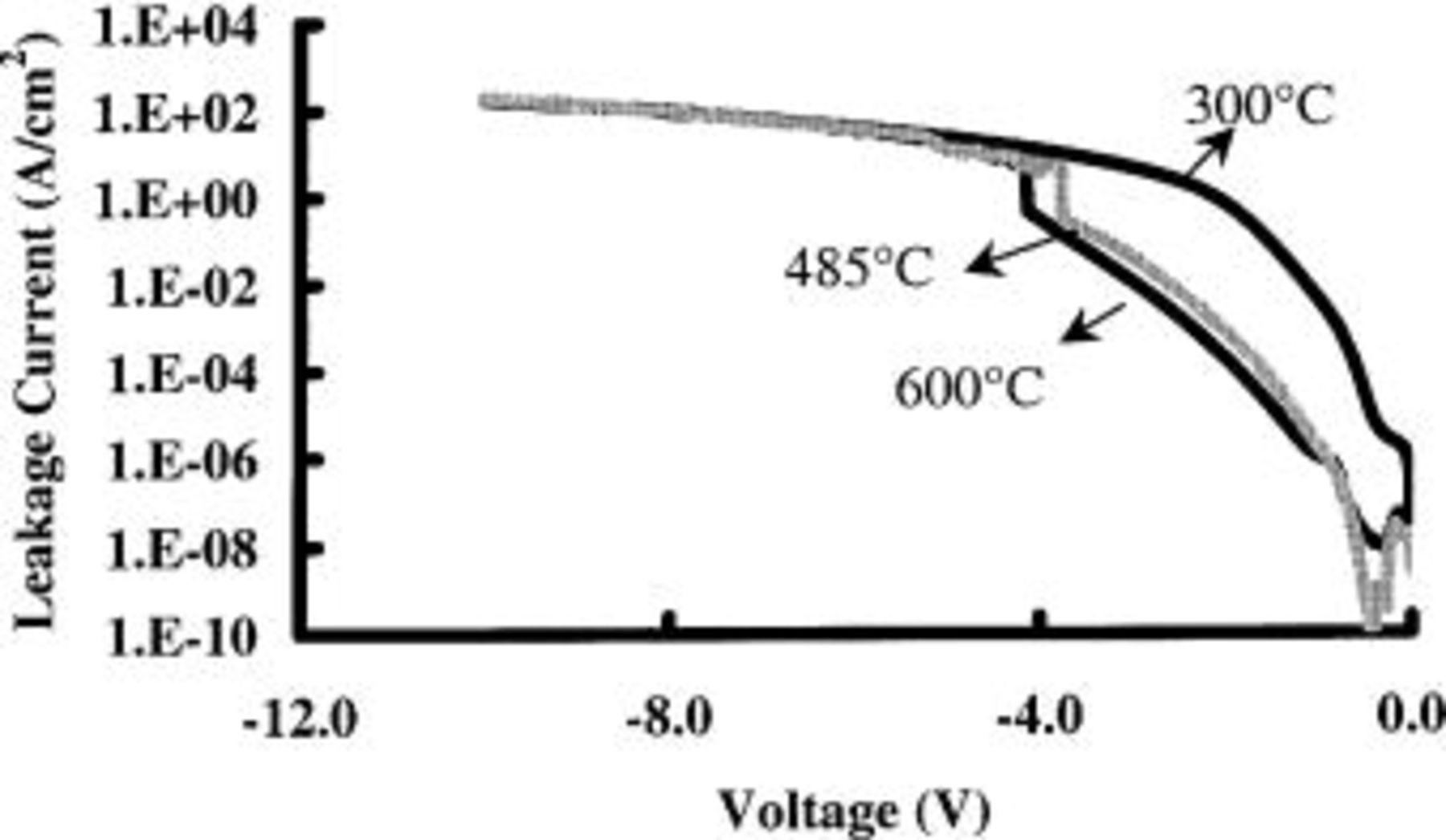
Figure 8. IV-curves for  -based gate stacks deposited at 300, 485, and 600°C. The layer deposited at 300°C clearly results in an inferior quality dielectric as compared to the films deposited at higher temperatures.
In addition, the starting surface also has an effect on the deposition and the resulting quality of the layers. When we compare the RBS determined Hf-dose for a deposition at 600°C on an RTO and HF-last starting surface (Fig. 9), it is clear that the deposition on the HF-last starting surface displays an incubation period, whereas the deposition on an RTO starting surface takes off almost immediately. This indicates that there is an inhibited growth for the HF-last starting surface that can result in deposited layers of a lower quality. As mentioned above, the HF-last starting surface results in a rougher top surface. Furthermore, this difference in surface preparation also results in a significant difference in electrical performance (Fig. 10). We compare two  cap/polySi stacks that are identical, except for their starting surface: a H-passivated starting surface (Fig. 10A) vs. an IMEC-clean
  starting surface (Fig. 10B). Although both stacks have an identical EOT (2.3 nm), it is clear that the leakage current density is substantially higher for the HF-last starting surface indicating it to be of a lower quality.
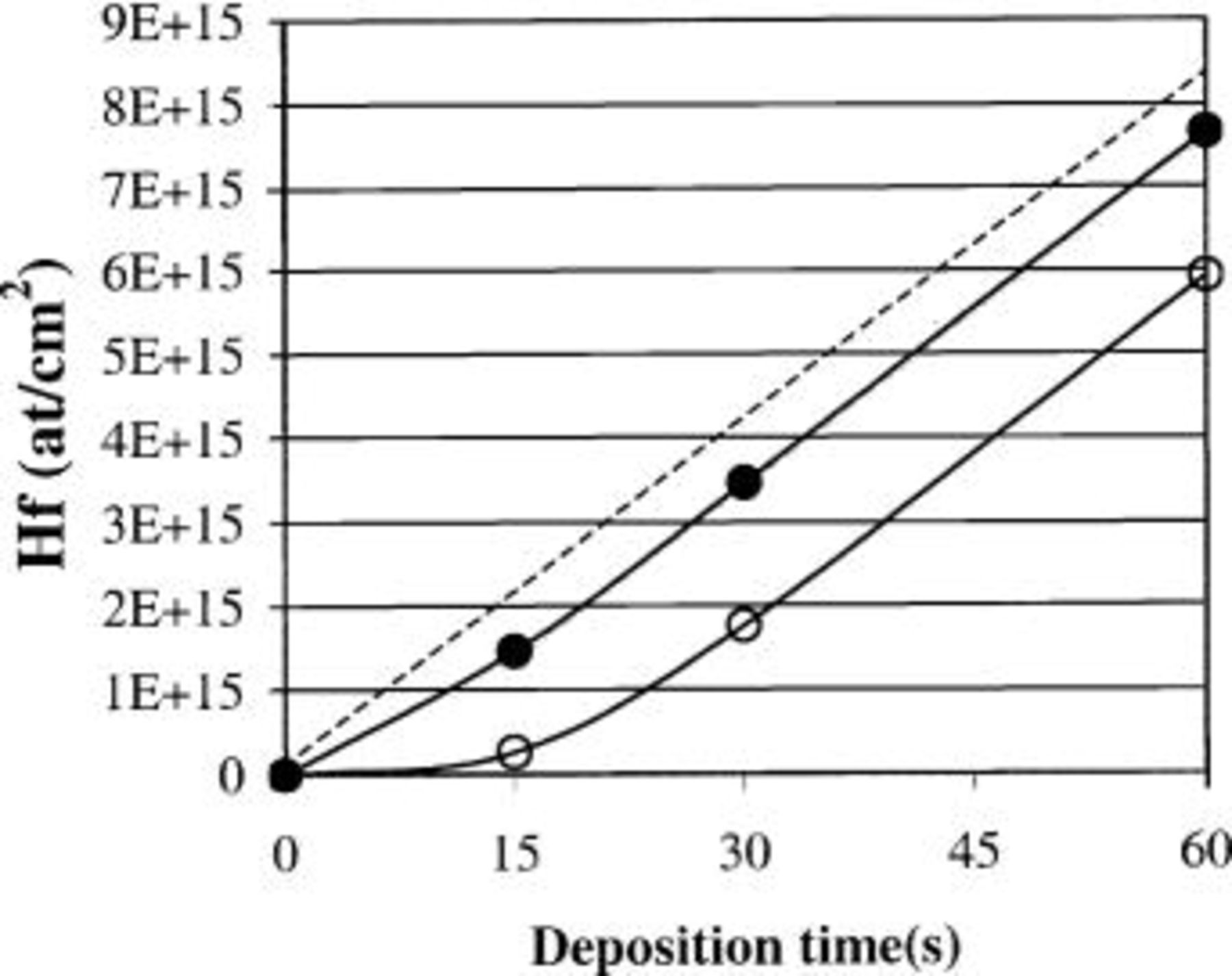
Figure 9. RBS-determined Hf dose for a deposition at 600°C on an HF-last and RTO starting surface. A clear growth inhibition can be observed for an HF-last starting surface (○) as compared to an RTO starting surface (•). The dashed line depicts a perfectly linear deposition starting at 

Figure 10. IV-curves measured on capacitors ranging from  to
to  for identical
  layer/polySi gate stacks on (A) an HF-last and (B) and oxide
  starting surface.
Density and organic contamination.—
The apparent low density of the layers as noted above suggests that these layers might have a porous structure. We used ellipsometric porosimetry to study this apparent porosity and attempted to quantify the percentage of pores present in the layers.22 After evacuating the pores in a vacuum chamber, the film is exposed to an adsorptive, in this case toluene. The adsorptive volume is calculated from the measured refractive index (in a system of open pores this adsorptive volume equals the total pore volume). For a thick  sample (∼100 nm thick) deposited at 485°C, the pore volume is determined to be 17-18%, where we can distinguish between micropores (0.5 nm) and mesopores (1.5 to 7 nm). This determined pore volume is in agreement with our density measurements, where we found that the thicker stacks deposited at 485°C or higher had a density of approximately 80% of the bulk value. To allow a fair comparison, we also determined the density for thinner samples, up to 80 nm thick, and obtained similar results. However, the EP technique is limited to very thick samples, and we were unsuccessful to extract reliable results for thin films.
Intuitively, it may be assumed that the presence of such pores can lead to possible contaminants in the films that are contained within these pores and originate from the deposition process or adsorption as a result of air exposure. We analyzed four 5 nm thick MOCVD  films with thermal desorption spectroscopy (TDS): two films were deposited at 300°C and two other films at 485°C. Two films (one of each deposition temperature) were analyzed approximately 1 h after deposition. The duplicate sample set was measured after a long period of clean room air exposure, i.e., approximately 3 months after deposition.
Figure 11 shows the quantity of desorbed  as a function of temperature. A 5 nm low-pressure chemical vapor deposited (LPCVD)
  is used as a blank sample (0.2 ppm background). It is clear that extended exposure to cleanroom air results in an increased (due to adsorption) amount of water contained in these layers, suggesting an open-pore structure (Fig. 11). Note that the high signals at elevated temperatures in Fig. 11b are due to a high background signal and decrease for each subsequent measurement to a similar level as observed in Fig. 11a.

Figure 11. Amount of water desorbing from the  films as a function of temperature measured (a) immediately after deposition and (b) after three months of storage. A 5 nm thick LPCVD nitride is used as a blank sample (x's). The film deposited at 485°C (▪) contains less
  than the film deposited at 300°C (○). Storage results in an increased amount of water. The low temperature of desorption indicates the water to be physisorbed.
The amount of water present in the first sample set (measured 1 h after deposition) is incorporated during the deposition or the short exposure to clean room atmosphere. The difference in the amount of moisture adsorption between samples measured 1 h after deposition and 3 months after deposition suggests that the samples after 1 h have not reached a state of equilibrium, which makes it very difficult to discuss the porosity based on the results for this sample set. The second sample set, however, can be assumed to be in a state of equilibrium because no additional adsorption is expected to occur after such a long time. Therefore, these results can be used to evaluate differences in porosity as function of the deposition temperature. The amount of desorbed water depends on the deposition temperature. The amount of desorbed water for the film deposited at 485°C is ∼38% less than that of the layer deposited at 300°C and much higher than the dense LPCVD  film (Fig. 11b). This observation correlates well with the observed difference in density.
A similar observation can be made for the levels of carbon present in the films. Figure 12 shows the signals for three different hydrocarbon ions: 
 and
and  (expressed as counts per second (cps)). It is clear that detectable levels of hydrocarbons are present in the films deposited at 300°C, while no carbon is detected for the films deposited at 485°C. These results were verified by TOFSIMS, where a clear C-profile was recorded throughout the sample deposited at 300°C, while the C-signal for the 485°C sample was below the detection limit (Fig. 13). A similar observation can be made for the N signal, which is significantly higher for the sample deposited at 300°C (not shown). The lower C- and N-levels at higher deposition temperatures may be explained by a more efficient oxidation of the precursor. Also note that a 5 min anneal at 900°C in a
  ambient does not remove the carbon present in the as-deposited layer.
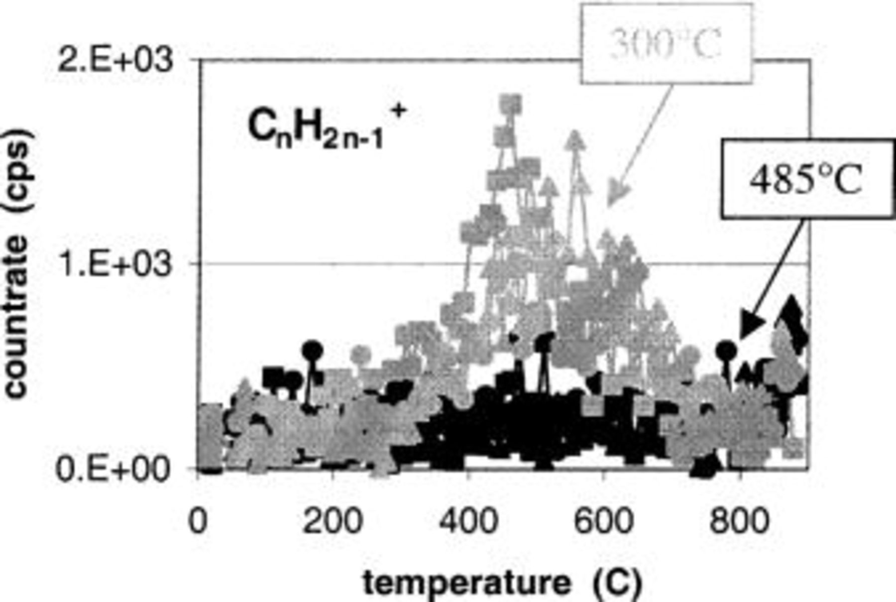
Figure 12. Amount of hydrocarbons that are desorbed from layers deposited at 300 and 485°C indicated by the gray and black markers, respectively. No hydrocarbons can be observed being desorbed from the layers deposited at 485°C, while a clear peak is seen for the 300°C deposited sample.
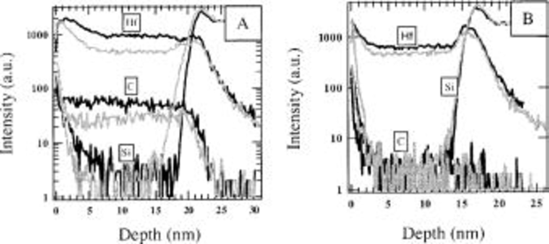
Figure 13. TOFSIMS depth profiles for  layers deposited at 300 (A) and 485°C (B) before (black curves) and after a 5 min 900°C
  anneal (gray curves).
Crystallization.—
Layers deposited as gate dielectric are preferably amorphous, because polycrystalline materials are suspected to give rise to an enhanced leakage and dopant diffusion along the grain boundaries. On the other hand, polycrystalline materials with very low gate leakages, for example  have been reported in literature
  for an EOT of 2.1 nm),23 therefore at present it is not yet clear if an amorphous layer is a real requirement.
 has a much lower crystallization onset temperature compared to
  Although it is possible to deposit an amorphous
  layer, it will likely crystallize upon further processing, especially during post-deposition anneals used to improve the quality of the layer.
  have a higher crystallization onset temperature that increases as a function of the Si content. Of course the k value of the material will decrease as a function of Si content making
  less interesting for high k applications, especially for the high performance applications that target very aggressive EOT specifications (<1 nm).
The crystallization behavior of MOCVD-deposited  is studied by means of XRD and ATR-FTIR. We found that the crystalline state of the
  depends on the deposition temperature, thickness, and post-deposition treatment. In Fig. 14, we show XRD spectra for 20 nm thick
  films deposited at 300 and 485°C before and after a 900°C
  5 min anneal. If we compare the spectra recorded for the as-deposited layers (Fig. 14a and c), then it is clear that the layer deposited at 300°C is amorphous while the layer deposited at 485°C is already polycrystalline as-deposited. Because of the limited number of observed diffraction peaks, they can be attributed to an orthorhombic or cubic phase. From these two the cubic phase is most likely due to the fact that orthorhombic is a high-pressure phase. After a 900°C, 5 min anneal in a
  ambient, the layers deposited at 300 and 485°C demonstrate similar spectra matching the monoclinic phase, indicating a phase transformation occurred during anneal. In Fig. 15 we used temperature controlled XRD measurements to study the crystallization onset temperature (COT) of the 300°C deposited film. The measurements were done on
  pieces that were heated under vacuum. Heating was done in 100°C increments and adequate time was given for the heated wafer to reach a state of thermodynamic equilibrium. From Fig. 15, it can be concluded that the sample crystallizes between 550 and 600°C. Other samples deposited in the temperature range between 300 and 420°C resulted in COT's between 600 and 800°C. These relatively high crystallization temperatures (compared to atomic layer deposited films) might be explained by the higher carbon content as observed by TOFSIMS. This would also be in agreement with the observation that layers deposited at 485°C are already crystalline as-deposited, and thus crystallize at lower temperature, because these layers have no carbon incorporated (below the detection limit).

Figure 14. XRD spectra of a  layer deposited at (a and b) 300°C and (c and d) 485°C before (a and c) and after (b and d) a 900°C,
  anneal (corresponding TEM of these layers are shown in Fig. 5).
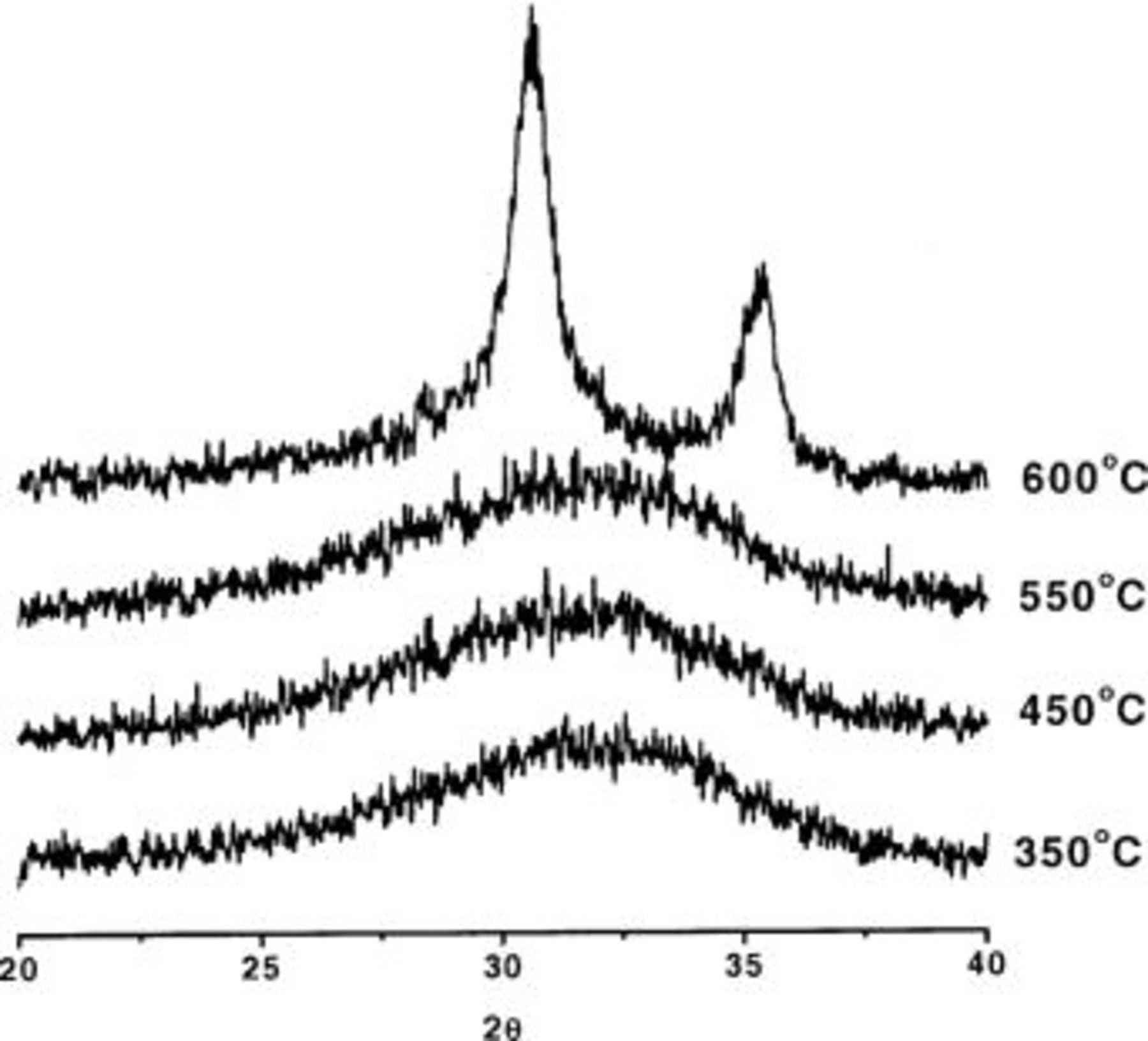
Figure 15. XRD spectra for a 20 nm thick  layer deposited at 300°C after heating in 100°C increments.
ATR-FTIR was also employed to study the crystallization behavior of these same  films since we have access to Hf-O stretching vibrations. In Fig. 16, we show the spectra recorded for the 300 and 485°C films before and after a 900°C,
  anneal. The features of the FTIR spectra recorded for the 300°C samples are very distinct from the 485°C samples. In the case of the as-deposited 300°C-sample (Fig. 16a), there is a single broad peak with a maximum at 690 cm−1, while for the as-deposited 485°C and both annealed samples show a clear doublet structure (2 peaks at 670 and 770 cm−1). The doublet structure is characteristic for a crystalline
  layer in a monoclinic phase.24 The peak positioned at 770 cm−1 is not as high when the layer is deposited at 300°C and annealed as when the film is deposited at 485°C. This may be related to the degree of crystallization of the layer. It is consistent with XRD results, where it is also shown that the film deposited at 485°C has a higher degree of crystallization. This demonstrates that ATR-FTIR can be used with a high degree of confidence to detect the crystallization of the
  layers.
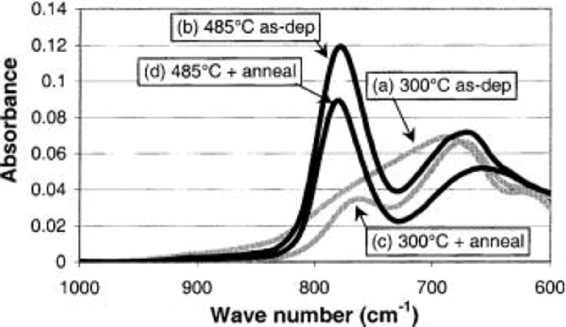
Figure 16. ATR-FTIR spectra for of  layers deposited at 300 and 485°C (identical sample set as shown in Fig. 14) as-deposited (a and b) and after a 5 min, 900°,
  anneal (c and d).
In addition to the effect of the deposition temperature and anneal on the crystallization behavior, the thickness of the layer has been found to have an effect on the crystallization temperature of the film. We compare FTIR spectra for a series of  layers with varying thickness all deposited at 485°C on an IMEC-clean starting surface (see Fig. 17). The thickness of the different layers (i.e., total thickness being
  layer) is listed in the figure as a label for the different spectra. Figure 17 shows that the thin layers are amorphous while the thicker layers are crystalline. Films remain amorphous up to a total thickness of 4.5 nm. A layer of 7.6 nm is crystalline which implicates that crystallization for a deposition temperature of 485°C starts from a layer thickness somewhere between 4.5 and 7.6 nm. Similar curves can be observed for a deposition temperature of 600°C, but at this temperature a layer of 4.8 nm is already crystalline (a layer of 3.6 nm is still amorphous).
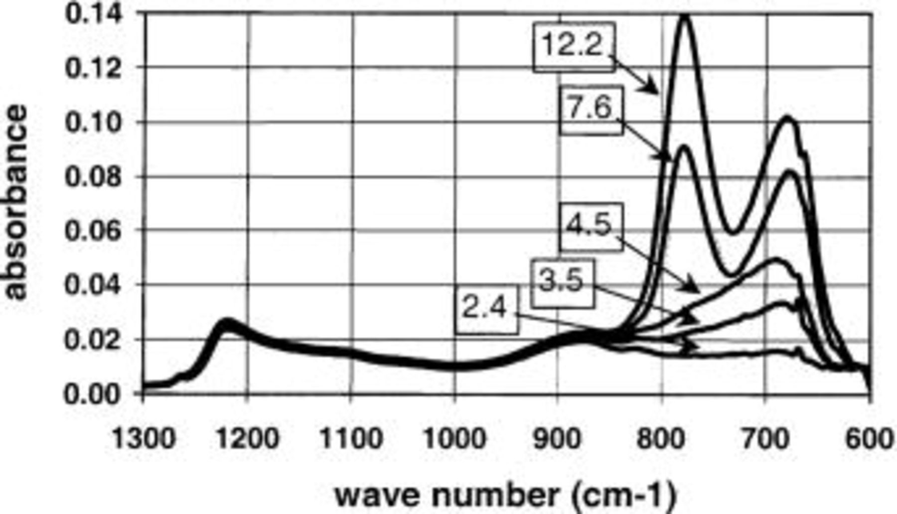
Figure 17. ATR-FTIR spectra for  layers deposited at 485°C on a IMEC-clean starting surface. The thickness of the total stack (in nm), as measured by ellipsometry, is used as label for the different spectra. It is clear that a minimum thickness is needed for the layer to be crystalline at 485°C.
Conclusions
In conclusion, the deposition of  layers with satisfactory dielectric properties requires a minimal deposition temperature that results in a polycrystalline layer, but with negligible carbon contamination. The density
  layers deposited via MOCVD are found to be less than 100% of the bulk value (9.68 g cm−3). Moreover, the starting surface is shown to have an affect on film density and in turn on the leakage characteristics of the film, where a chemical oxide starting surface results in the higher quality film. A major concern with these films is the low density of the thin layers with respect to gate dielectric applications. It is expected that the low density will heavily deteriorate the dielectric properties and thereby limit scalability of the material.
Acknowledgments
All ATR-FTIR measurements were done at LETI, France. In this respect, we especially thank Nevine Rochat for his valuable contribution developing the ATR-FTR technique at LETI, France.
IMEC assisted in meeting the publication costs of this article.