
Abstract
We have systematically investigated the electronic structure of CeO2 dielectric by plasma enhanced atomic layer deposition (PE-ALD). The CeO2 films were deposited by using novel tris(isopropyl-cyclopentadienyl)cerium [Ce(iPrCp)3] precursor and O2 plasma. The energy band gap (3.48 eV), Fermi level (4.71 eV), and band offsets of PE-ALD CeO2 were elaborately determined by combining spectroscopic ellipsometry and ultraviolet photoemission spectroscopy (UPS) techniques. In addition, based on the experimental results of Fowler-Nordheim(F-N) tunneling and Poole-Frenkel(P-F) conduction for Al/PE-ALD CeO2/p-Si, the increased interfacial layer and reduced trapped oxide densities were found to be correlated to the increase in effective barrier height (0.89, 1.18 and 1.26 eV) and decrease in decreased trap energy levels (0.47, 0.26 and 0.18 eV) with increasing O2 annealing temperature (400, 600 and 800°C), respectively. These discrepancies might be attributed to the thin film characteristics and oxygen vacancies in the CeO2 dielectrics, depending on the deposition techniques and post deposition annealing processes.
Export citation and abstract BibTeX RIS
With aggressive scaling of complementary metal-oxide-semiconductor (CMOS) technologies, high-k dielectric has become a front up choice to replace conventional SiO2 beyond sub-45 nm technology.1, 2 Among various high-k gate oxides, Cerium oxide (CeO2) is an attractive candidate as a gate dielectric material, due to high dielectric constant (23–52), high refractive index (2.2–2.8), high dielectric strength (∼25 MV/cm), moderate bandgap (3.0–3.6 eV), and small lattice mismatch (∼0.35%) as well as thermodynamical stability in contact with Si.3–5 More recently, the doping effects of CeO2 in HfO2 or vice versa were investigated to stabilize the phases with high permittivity or reduce the leakage current densities.6, 7 Due to its technical importance on various research fields, various thin film deposition techniques including physical vapor deposition (PVD) and chemical vapor deposition (CVD) have been studied to deposit the CeO2 films.8–11
However, as the modern integrated devices are scaling down, the need for a deposition technique to produce high quality films with nanoscale thickness controllability is tremendous. Regarding this, atomic layer deposition (ALD) has received a great deal of attention as a promising deposition method especially for high k dielectrics, mainly due to its benefits such as thickness uniformity and atomic scale thickness and composition controllability.12 So far, only a few research groups have reported ALD CeO2 thin films, and their reports have been simply focused on the growth characteristics of ALD CeO2.13, 14 In particular, the current transport mechanisms and electronic structures for MOS structures using ALD CeO2 dielectrics have not been reported yet in spite of its potential importance as a gate dielectric. The carrier transports through CeO2 films are strongly affected by the deposition method and process parameters, but previous studies on carrier transports through CeO2 films have been devoted only to evaporation and sputtering methods.5, 15 Nevertheless, the comprehensive studies including the optical and electrical properties to understand entire electronic structures still have not been addressed in detail. Further, there are some undesirable properties of CeO2 dielectric, such as high hysteresis.16, 17 Generally, the electrical properties of high k dielectrics have been improved by performing a post-deposition annealing (PDA) at various temperatures.18, 19 It prompts us to investigate the effects of PDA temperature on carrier transports in CeO2 dielectric.
In this study, for the first time, we have comprehensively investigated the electronic structure of our recent plasma enhanced atomic layer deposition (PE-ALD) CeO2 films by combining the spectroscopic ellipsometry and photoemission spectroscopy techniques. Furthermore, we observed the changes of electron carrier transports with increasing O2 annealing temperatures from 400 to 800°C by evaluating Fowler-Nordheim (F-N) tunneling and Poole-Frenkel (P-F) conduction for Al/CeO2/p-Si structure, and thereby deduced the entire energy band diagram.
Experimental
For this study, a commercial PE-ALD chamber (SNTEK Co., ALD5008) composed of a main chamber and a loadlock was utilized. This system has a double shower head system for good uniformity with plasma capability, which consists of two pieces laid in a fold; upper one for precursor dose and lower one for reactant exposure. The lower showerhead part was connected to a radio-frequency (RF) plasma generator with matching network. Thus, the specimen on the substrate heater was directly exposed to the plasma generated during the reactant pulse. Further information on the same type of chamber configuration can be found in our previous report.20
More recently, we reported the growth characteristics and film properties of PE-ALD CeO2 films using the newly developed tris(isopropyl-cyclopentadienyl)cerium [Ce(iPrCp)3] as a Ce precursor.21 Accordingly, the Ce(iPrCp)3 was employed as a Ce precursor in this study. Based upon our thermogravimetric-differential thermal analysis (TG-DTA) data,21 the Ce(iPrCp)3 precursor contained in a stainless steel bubbler was evaporated at a temperature of 135°C to produce high enough vapor pressure and the delivery lines were heated to 10–15°C higher temperature than the bubbler to prevent the Ce precursor condensation. The Ce(iPrCp)3 vapors were carried into the reaction chamber by Ar carrier gas whose flow rate was controlled by mass flow controller (MFC). Ar gas with the same flow rate was also used for purging of excess gas molecules and byproducts between each precursor and reactant exposure steps. For PE-ALD, oxygen gas controlled by MFC was flown into the showerhead, where the plasma was turned on only during the O2 exposure step with a constant plasma power of 300 W. During the PE-ALD process, the substrate temperature was maintained at 250°C.
For MOS capacitor fabrication, 12 nm thick CeO2 films were deposited on p-type Si (ρ = 5–20 Ω cm) substrates, which were cleaned at 70°C for 10 min in RCA solution (1:1:5(v/v/v) NH4OH/H2O2/H2O), followed by dipping in buffered oxide enchant solution for 30 s to remove native oxide. After the oxide deposition, PDA was carried out by rapid thermal annealing (RTA) system in an O2 ambient at 400, 600 and 800°C for 10 min. Then, Al was thermally evaporated as a metal gate through a dot-pattered shadow mask with a radius of 100 μm and Au was also thermally evaporated as a back contact material.
The film thickness and refractive index of the CeO2 film were measured by spectroscopic ellipsometry. The work function of CeO2 film was investigated by ultraviolet photoemission spectroscopy (UPS) with He I emission of 21.2 eV. The electrical properties including C–V and I–V characteristics were evaluated by HP4284 LCR meter and Agilent 4155C semiconductor parameter analyzer. To overcome the measurement problems associated with series resistance and leakage currents, capacitance values were extracted from a resistance correction procedure.22 For this, the capacitances were measured at two different measurement frequencies (10 and 100 kHz) and the actual frequency-independent capacitances were obtained using the following equation
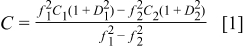
where Di is a dissipation defined by Gi/ωCi measured at frequency fi, Gi is a conductance at frequency fi and ω is angular velocity (=2πfi). The interface state density Dit was determined by conductance method. For this, conductance Gp versus voltage and frequency was measured at various frequencies from 1 kHz to 1 MHz. Measured Gp values were corrected by taking series resistance and insulator capacitance into account.17 Conductance loss (Gp/ω) was selected at maximum value in swept voltage. The Dit value was extracted by the following equation23
where Gp/ω is a corrected conductance loss, ω is an angular frequency (ω = 2πf, f is the measurement frequency), q is an electronic charge (1.6 × 10¹⁹ C), fD is a universal function as a function of standard deviation of band banding σs, and A is an area of metal gate. For general high k gate dielectrics, the fD is 0.35–0.4.23
Results and Discussion
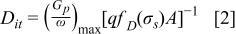
To begin with, the spectroscopic ellipsometry spectra of Fig. 1a shows the real (n) and imaginary (k) parts of the refractive index measured in the energy range of 1.5–4.0 eV for the PE-ALD CeO2 film. The refractive index n of the CeO2 film was determined to be 2.28 ± 0.05 at wavelength of 632.8 nm, which is comparable to previously reported values.16, 24 From the extracted k value, the absorption coefficient α was determined from the simple relation, α = 4πk/λ. Accordingly, the plot of (αhν)2 vs hν (photon energy) is shown in Fig. 1b. Here, the optical band gap (Eg) was obtained from the intercept position by extrapolating the linear part of the curves down to the photon energy axis. The Eg was determined to be 3.48 eV, which is within the range of reported values (3.0–3.6 eV) prepared by sputter or evaporation elsewhere.5, 8
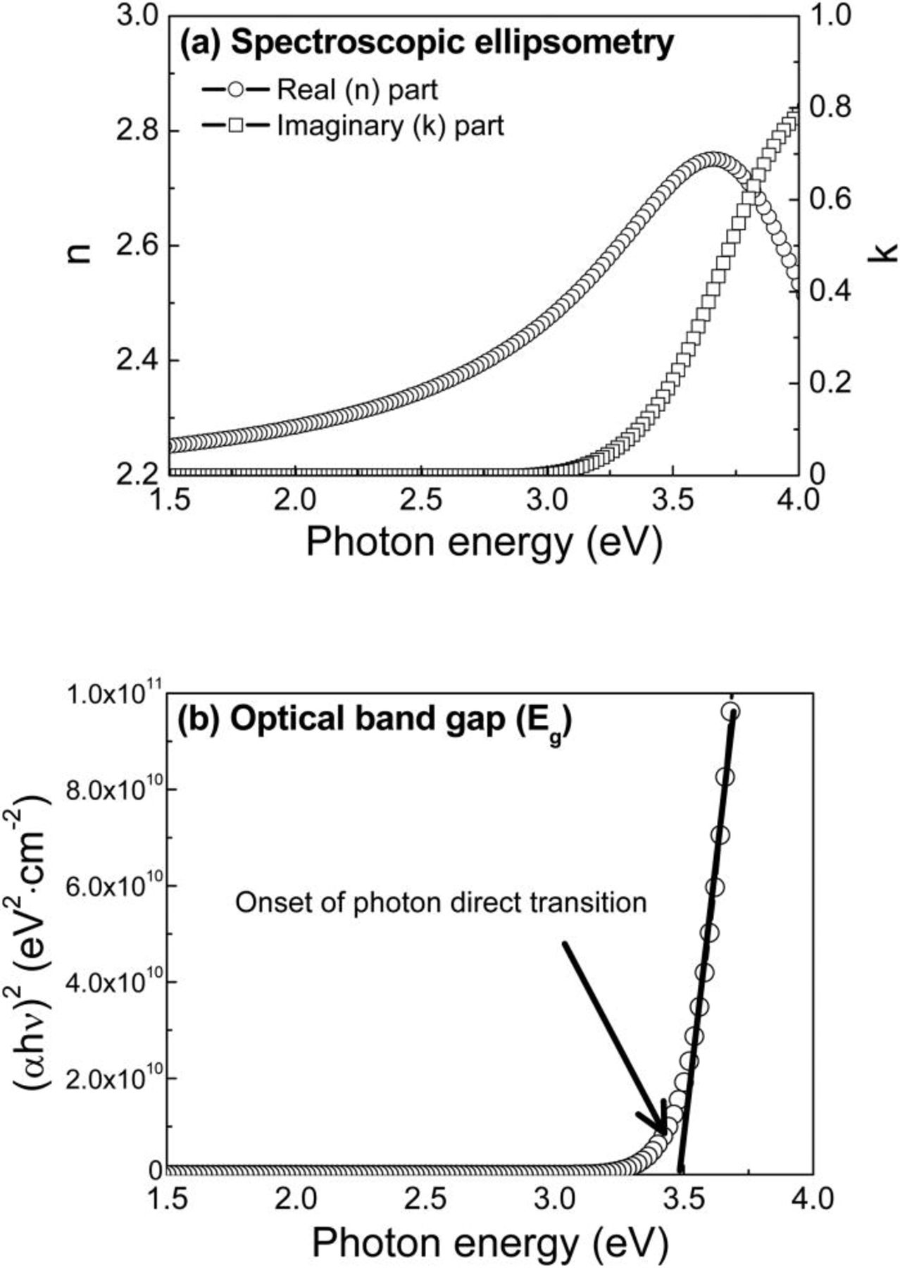
Figure 1. (a) Spectroscopic ellipsometry data: real and imaginary parts of refractive index, and (b) Plot of (αhν)2 vs photon energy for the PE-ALD CeO2 film.
Next, UPS analysis was conducted to elaborately determine the positions of the conduction band minimum (ECB), valence band maximum (EVB), and Fermi level (EF). The relationship between several energy levels (Ecutoff, EVB, EF, and Evac) is shown in the UPS spectrum of Fig. 2. The work function (Φ) of the film was extracted by secondary electron cutoff method using the following equation25

where Ecutoff is the secondary electron cutoff; the other terms are as defined above. The work function was estimated to be ∼4.71 eV and the difference between valance band edge and Fermi level was estimated to be ∼2.03 eV by the linear extrapolation indicated in the spectrum. Based on the relationship determined by ellipsometer and UPS methods, the band position was determined precisely as illustrated in inset of Fig. 2.
Figure 2. UPS spectrum of the PE-ALD CeO2 film [inset: the schematic drawing of energy band position].
Figure 3a shows the C-V curves of the MOS capacitors with the PE-ALD CeO2 gate dielectrics annealed at 400, 600 and 800°C in the O2 ambient. With increasing O2 annealing temperature, maximum accumulation capacitances were decreased due to the growth of the interfacial layer between CeO2 and Si. The dielectric constants of total oxide layers were 14.8, 13.3 and 12.4, respectively, for 400, 600, and 800°C. In addition, a negative flatband voltage shift (ΔVFB) was observed in all of MOS capacitors, suggesting the presence of a positive effective oxide charge Qeff in the oxide.19 As the O2 annealing temperature increases, it is effectively reduced, comparable with previous reports on CeO2 films.19, 21, 26 The inset of Fig. 3a reveals the changes of trapped oxide charge density Not and Dit according to O2 annealing temperature. From the hysteresis obtained by sweeping the voltage from accumulation to inversion and back again, the Not values were calculated from the measured hysteresis by the following equation
where ΔVFB is a hysteresis width, Cacc is the accumulation capacitance, q is the electronic charge (1.60218 × 10⁻¹⁹ C), and A is the electrode area. It is clearly seen that a hysteresis is reduced with increasing annealing temperature, resulting in the decrease of the measured trapped oxide charge densities from 1.2 × 10¹², 2.3 × 10¹¹, to 8.6 × 1010 cm−2. The reduction in Not with increasing the annealing temperature is mainly attributed to the reduced oxygen vacancies as positively charged defect centers in the bulk oxide.27 The Dit values were also reduced by annealing (7.8 × 10¹¹, 5.3 × 10¹¹, and 3.4 × 1011 cm−2 eV−1, respectively, for 400, 600 and 800°C), which were determined by the conductance method stated in our previous publication.28 The comparable trend and values by annealing were found elsewhere.19 In addition, Fig. 3b exhibits the gate leakage current densities as a function of gate bias as a function of annealing temperatures. With increasing the annealing temperature, the leakage current densities were reduced; 7.3 × 10⁻⁷, 2.9 × 10⁻⁷ and 1.1 × 10⁻⁷ A/cm2 for 400, 600 and 800°C annealed samples, respectively, at VFB-1V. It was believed that the reduced leakage properties are mainly due to the decreased Not and Dit as well as the increased interfacial layer.19
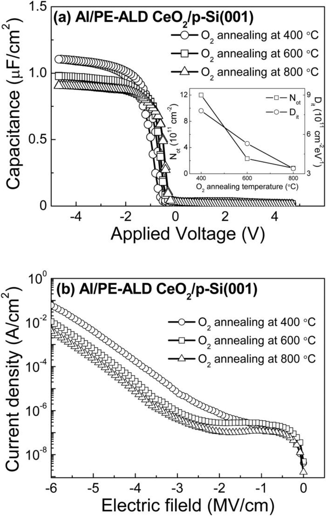
Figure 3. (a) Capacitance-voltage curves [inset: trapped oxide charge Not and interface state density Dit] and (b) Gate leakage currents of the three MOS capacitors with PE-ALD CeO2 annealed at 400, 600 and 800°C.
To determine the electron carrier transport between Al and CeO2 for the three MOS samples, the gate leakage current density at high field region was fitted to F-N tunneling equation, as shown in Fig. 4a. The F-N tunneling is given by the following expression29
where A is the constant unity, E is the electric field, mox is the electron effective mass, Φb (qϕb) is the electron barrier height (conduction band offset) between Al and CeO2, q is the electronic charge and h is the Planck constant. The fitted line slope of Ln(J/E2) versus 1/E yields the conduction band offset between Al and CeO2. Thereby, the effective values of electron barrier height were obtained to be 0.89, 1.18 and 1.26 eV for 400, 600 and 800°C annealing samples, respectively. It suggests that the reduced defect densities and increased interfacial layer with increasing the annealing temperature resulted in the increase in the effective values for the electron barrier height.30
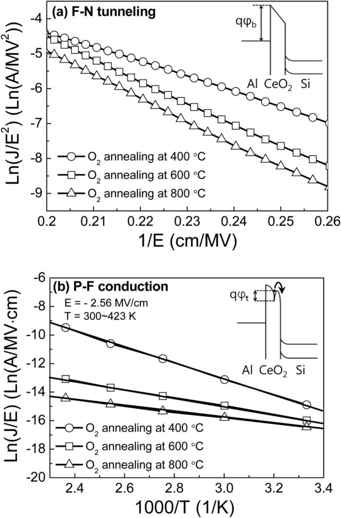
Figure 4. (a) F-N tunneling fitting in the high field region of the leakage currents and (b) P-F conduction fitting from the leakage currents measured at temperature ranges from 300 to 423 K [insets: the schematic drawings of energy band diagram of conduction band region showing the energy barrier levels of Φb and Φt].
Meanwhile, the high-k oxide films have many traps, isolated states and smaller band gap than the conventional SiO2 films.31 Accordingly, the currents flow through the trap sites if the electrons in the gate electrodes can obtain enough energy to overcome the Schottky barrier. The required energy is provided by thermal activation. The internal thermionic emission through the trap sites is P-F conduction, which is highly probable to be related to oxygen vacancies of divacancies in high-k oxide films.32, 33 Hence, to elucidate the electron carrier transport through these trapped charges in the three kinds of CeO2 dielectrics, the P-F conduction fitting was conducted from the leakage currents measured at various temperature ranges from 300 to 423 K, as shown in Fig. 4b. The P-F conduction mechanism is defined by the following equation34
where B is the constant proportional to the density of bulk oxide traps, Φt (qϕt) is the trap energy level, ɛr is the dynamic dielectric constant (the square of the measured refractive index, ɛr = n2 = 5.19), ɛo is the free-space permittivity, and k is the Boltzmann constant; the other notations are defined above. The fitted line slope of Ln(J/E) versus 1000/T yields the trap energy levels from the conduction band of CeO2, effective values of which were determined to be 0.47, 0.26 and 0.18 eV for 400, 600 and 800°C annealed samples, respectively. In other words, these trap energy levels related to oxygen vacancies or divacancies becomes smaller with increasing the annealing temperature. Thus, it indicates that most of the trap charges would be effectively eliminated by a high temperature annealing up to 800°C.
The discrepancies in the conduction band offset and trap energy level might be strongly related to the thin film characteristics and oxygen vacancies formed in the CeO2 dielectrics depending on the deposition techniques and post deposition annealing processes. Therefore, based on all the experimental results, we have estimated the entire energy band diagram of Al/CeO2/p-Si MOS structure with constant Fermi level at thermal equilibrium for 400°C annealed sample, the schematic drawing of which is shown in Fig. 5. It serves to summarize the key results that we have obtained from ellipsometry and UPS spectra, F-N tunneling and P-F conduction. In particular, it is worthy to note that current PE-ALD CeO2 is more beneficial for the improved dielectric properties judging from Eg, Φb and Φt values, compared to the previous results.5, 15
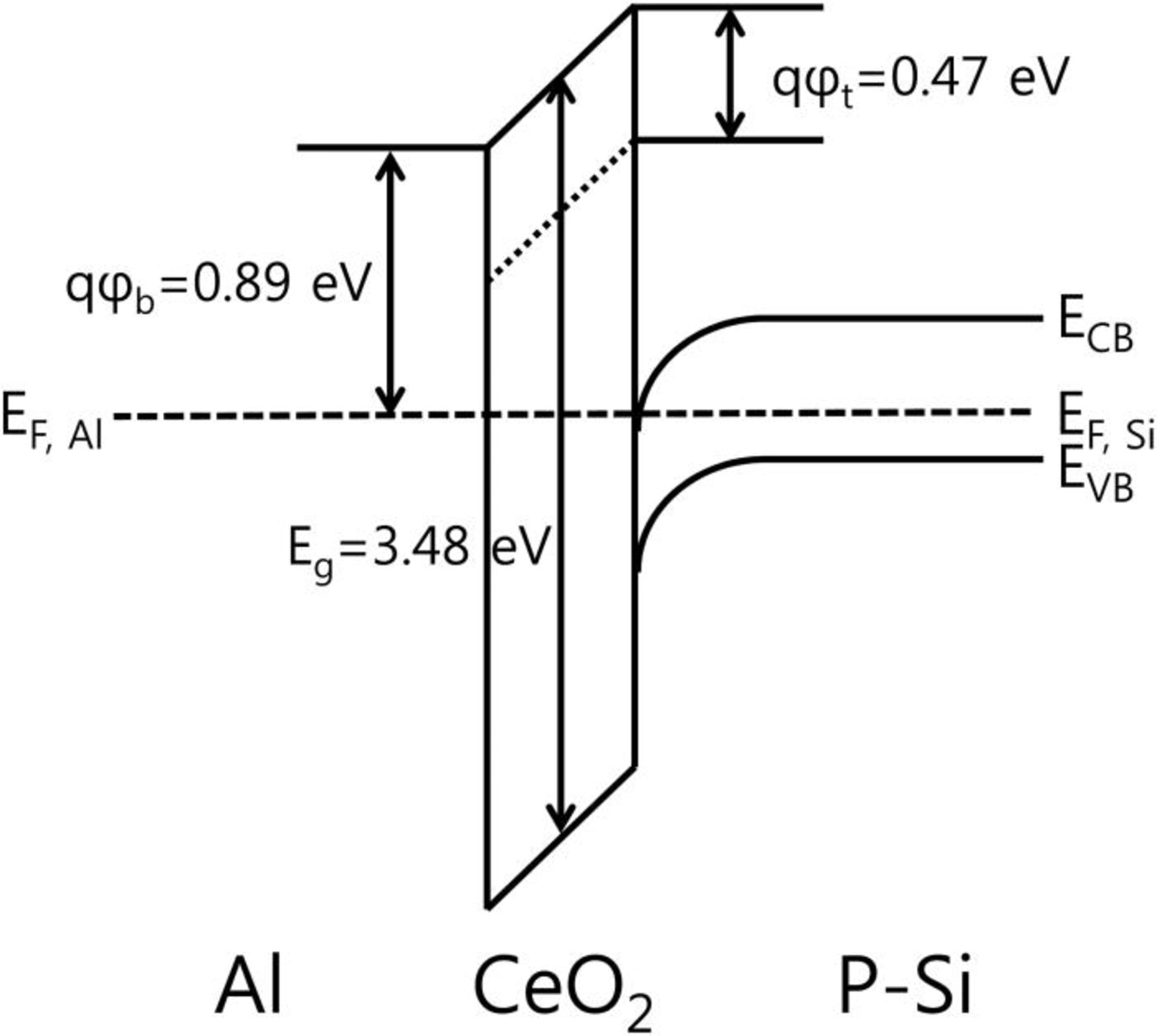
Figure 5. The schematic drawing for energy band diagram of Al/CeO2/p-Si MOS structure sample annealed at 400°C at thermal equilibrium.
Conclusions
For this study, systematic investigations were conducted to comprehensively demonstrate the energy band diagram including the electron carrier transports for Al/PE-ALD CeO2/p-Si structure for the first time. For the PE-ALD CeO2 film, the energy band gap of 3.48 eV and its precise position were determined by combining the ellipsometry and UPS techniques. From the results on F-N tunneling and P-F conduction characteristics of MOS capacitors, as increasing the O2 annealing temperature, the effective barrier height Φb at Al/CeO2 interface was increased, whereas the effective trap energy level Φt was decreased. The main reasons for these characteristics are found to be due to the increased interfacial layer and reduced trapped oxide densities with increasing the annealing temperature.
ACKNOWLEDGMENTS
This work was supported by Applied Materials 1st stage project. This work was also supported by the Technology Innovation Program funded by the Ministry of Knowledge Economy (MKE, Korea, No. 10030519) and by Nano R&D program through the National Research Foundation of Korea (NRF) funded by the Ministry of Education, Science and Technology (No. 2010-0020230).