Abstract
An MOS transistor fabricated on (001) β-Ga2O3 exfoliated from a commercial (−201) β-Ga2O3 substrate is reported. A maximum drain current of 11.1 mA/mm was measured, and a non-destructive breakdown was reached around 80 V in the off state. Threshold voltage of +2.9 V was extracted at 0.1 V drain bias, and peak transconductance of 0.18 mS/mm was measured at VDS = 1 V, corresponding to a field effect mobility of 0.17 cm2/Vs. Hall effect and electron spin resonance data suggested that electron conductivity was due primarily to O vacancy donors (VO+) with an estimated density of 2.3 × 10¹⁷ (±50%) cm−3.
Export citation and abstract BibTeX RIS

This is an open access article distributed under the terms of the Creative Commons Attribution 4.0 License (CC BY, http://creativecommons.org/licenses/by/4.0/), which permits unrestricted reuse of the work in any medium, provided the original work is properly cited.
The single-crystal monoclinic (β) phase of Ga2O3 is an advantageous material for high-power, high-temperature electronic device applications due to its high energy gap (4.8–4.9 eV) and high breakdown field (8 MV/cm), yielding a nearly ten-fold higher Baliga figure of merit than that of 4H-SiC (BFOMGa2O3 = 3444, BFOM4H-SiC = 300).1 Commercially available β-Ga2O3 substrates enable the epitaxial growth of low defect density epitaxial β-Ga2O3 by a number of methods, including chemical vapor deposition, hydride vapor phase epitaxy (HVPE), and molecular beam epitaxy (MBE), among others.2–6 Schottky barrier diodes (SBDs) based on Ga2O3 have exhibited very low turn on voltage and reverse leakage current, suggesting that unintentionally doped Ga2O3 has extremely low generation/recombination rates and thus a high photoconductive gain.7 Advances in doping control have enabled exceptional early reports of metal- and metal-insulator-gated field effect transistors (MOSFETs). Wong et al. demonstrated a field-plated β-Ga2O3 MOSFET with a breakdown voltage of over 750 V using a Si-implanted channel.8 Most recently, Green and coworkers have reported a Ga2O3 MOSFET with a Sn-doped channel and a 0.6 μm gate-drain spacing to operate at 200 V drain bias, experimentally demonstrating gate-drain fields in excess of 3 MV/cm.9 This excellent progress has positioned Ga2O3 as a viable candidate for next generation material for power applications. However, no demonstration of normally-off operation, a key requirement for fail-safe operation of power switches, has been achieved or proposed to-date.
From a practical perspective, development of Ga2O3 transistors has been limited by the availability of device-quality epitaxial films. For this reason, early reports have exploited the relatively large a-plane lattice constant of β-Ga2O3 (1.2 nm) in order to mechanically exfoliate thin films from the (001) plane of a substrate using the scotch tape method to fabricate back-gated devices.10,11 We employed a similar method to transfer a thin (∼300 nm) Ga2O3 flake onto a SiO2/Si substrate,12 and performed a standard top-side insulated-gate process to fabricate a three-terminal device. We also utilized a high-k HfO2 gate dielectric process, as only SiO2 and Al2O3 have been reported to-date.13,14
Experimental
A thin sliver of Ga2O3 was cleaved along the (001) face of an on-axis (−201), non-intentionally n-type doped (∼3 × 1017 cm−3) commercial Ga2O3 substrate (Tamura Corporation) produced by the edge-defined film fed (EFF) growth method. The cleaved material was verified to be of the (001) orientation by X-ray diffraction (XRD, Fig. 1), and was further thinned by repeated exfoliation using Nitto Denko Revalpha thermal release tape.12 The target SiO2/Si substrate was cleaned in a SAMCO UV-1 ozone system for 10 min. at room temperature. The tape was then pressed onto the substrate and upon a final exfoliation the transferred Ga2O3 flake was approximately 300 nm thick and 11.7 μm wide. Ohmic contacts of Ti/Au (20/200 nm) were lifted off on both ends of the sample, followed by atomic layer deposition (ALD) of a 42 nm thick HfO2 gate dielectric, and a 20/200 nm thick Ni/Au gate lifted off using standard photolithography techniques. No implantation or rapid-thermal annealing were performed, and cleaning prior to metal and dielectric deposition consisted of a 10 min. UV-O3 treatment. The as-processed transistor, depicted in the inset of Fig. 1, had a gate length of 3 μm, a gate-source spacing of 2 μm, and a gate-drain spacing of 5 μm.
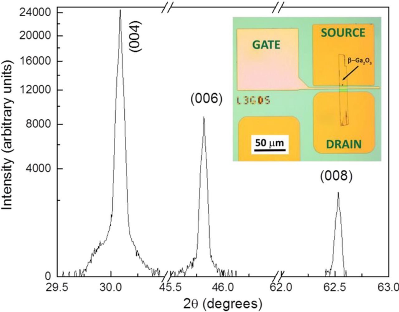
Figure 1. X-ray diffraction spectra of the (001) Ga2O3 flake exfoliated from a (−201) Ga2O3 substrate. Inset: optical image of the fabricated top-gated transistor.
Capacitance-voltage and current-voltage measurements were performed using a Keithley 4200 and a HP4145b analyzers, respectively. Hall effect measurements were performed using a closed-circuit He-cooled Lakeshore Hall probe station with a superconducting magnet (±0.5 T magnetic field used in this work). The electron spin resonance (ESR) measurements were done at 300 K with a commercial (E-300) Bruker Biospin 9.5 GHz spectrometer. Estimates of the spin concentrations were made from double numerical integration of fits to the ESR lineshapes and the use of a well-calibrated P-doped Si standard.
Results and Discussion
Gate capacitance-voltage characteristics measured as a function of frequency and voltage with the source-drain contacts connected together is presented in Fig. 2. The inhomogeneity of the depletion capacitance was indicative of traps present at the HfO2/Ga2O3 interface. The flatband voltage, determined by the flatband capacitance CFB = 0.8 CMAX, was approximately VFB ≅ +2 V for the 300 kHz measurement.15 To our knowledge, this is the first report of a positive threshold voltage measured for a β-Ga2O3 MOS interface, and presently speculate that it originated from a larger conduction band offset between HfO2 and β-Ga2O3, beyond the values of 3.1 ± 0.2 eV and 1.5 ± 0.2 eV reported for the SiO2 and Al2O3 interfaces with Ga2O3, respectively.13,14 Further X-ray photoelectron spectroscopy measurements will be performed to accurately determine the band offsets for this novel dielectric interface.
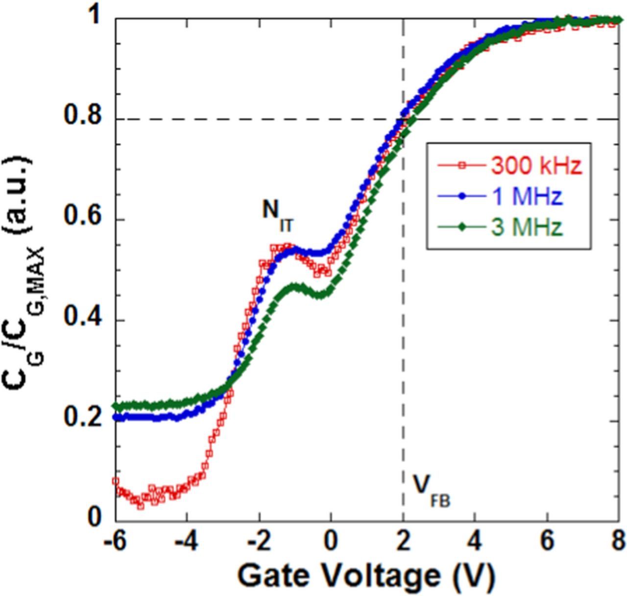
Figure 2. Capacitance-voltage profile of the gate capacitance as a function of frequency for the Ga2O3 transistor.
The static dc current-voltage measurements of the as-fabricated MOSFET are presented in Fig. 3. A maximum drain-source current (IDS,SAT) of about 11.1 mA/mm and an on resistance (RDS,ON) of about 818 Ω-mm were measured in the on-state at a forward gate bias of +18 V (Fig. 3a). Significant off-state current leakage was present for gate biases of 0 V and below, and could originate from the traps at the HfO2/Ga2O3 or the Ga2O3/SiO2 interfaces, or from drain-induced barrier lowering (DIBL) owing to the absence of n+ doped source/drain regions. The positive VT, observed at 100 mV drain bias when IDS was measured as a function of VGS in Fig. 3b, was determined to be +2.9 V using a linear fit of the IDS. Increasing the drain bias clearly lowered the barrier to electron accumulation and pushed the device back toward depletion mode. The peak transconductance at VDS = 1 V was 0.18 mS/mm, and a field effect mobility of 0.17 cm2/Vs was calculated using the relationship μFE = gm·(L/W)/(COX·VDS).11 Fig. 3c shows that the gate current remained low (10–100 pA) up to the maximum non-destructive drain bias applied to the device. At 80 V, the off-state drain current significantly increased, however, this non-catastrophic breakdown was gate bias dependent and was thus not determined by the theoretical critical field of Ga2O3 (8 MV/cm).
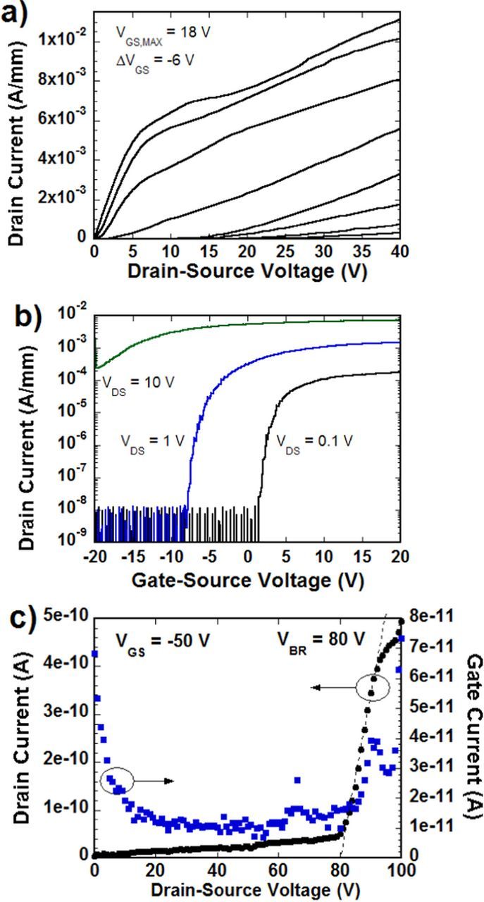
Figure 3. a) DC output (IDS-VDS) characteristics, b) DC input (IDS-VGS) as a function of drain bias (0.1, 1, and 10 V), and c) Off-state IDS-VDS characteristic showing the soft breakdown regime at around 80 V.
Due to the restrictions posed by the mechanical exfoliation process, it was not possible to measure device parameters such as channel electron density and contact resistance, which would necessitate additional test structures (van der Pauw, TLM). In order to mitigate this limitation, temperature-dependent Hall effect measurements were performed on a square 8 × 8 × 0.68 mm sample of (−201) Ga2O3 with evaporated Ti/Au contacts in each corner and data is presented in Fig. 4a. To-date, Hall data has been reported by Parisini and Fornari for Czochralski-grown Ga2O3, and by Oishi and coworkers for EFF-grown Ga2O3.16,17 Both Parisini and Oishi reported peak mobilities around 85 K with respective values of ∼600 cm2/V·s and 886 cm2/V·s, respectively. However, for the sample with a similar doping level to ours (3 × 1017 cm−3 at 300 K), Parisini measured a peak Hall mobility of about 300 cm2/V·s at 100 K. Our measurements indicated a peak mobility of 348 cm2/V·s at 140 K, which was consistent with the reported limits by optical phonon scattering at high temperature and ionized impurity scattering at low temperature.
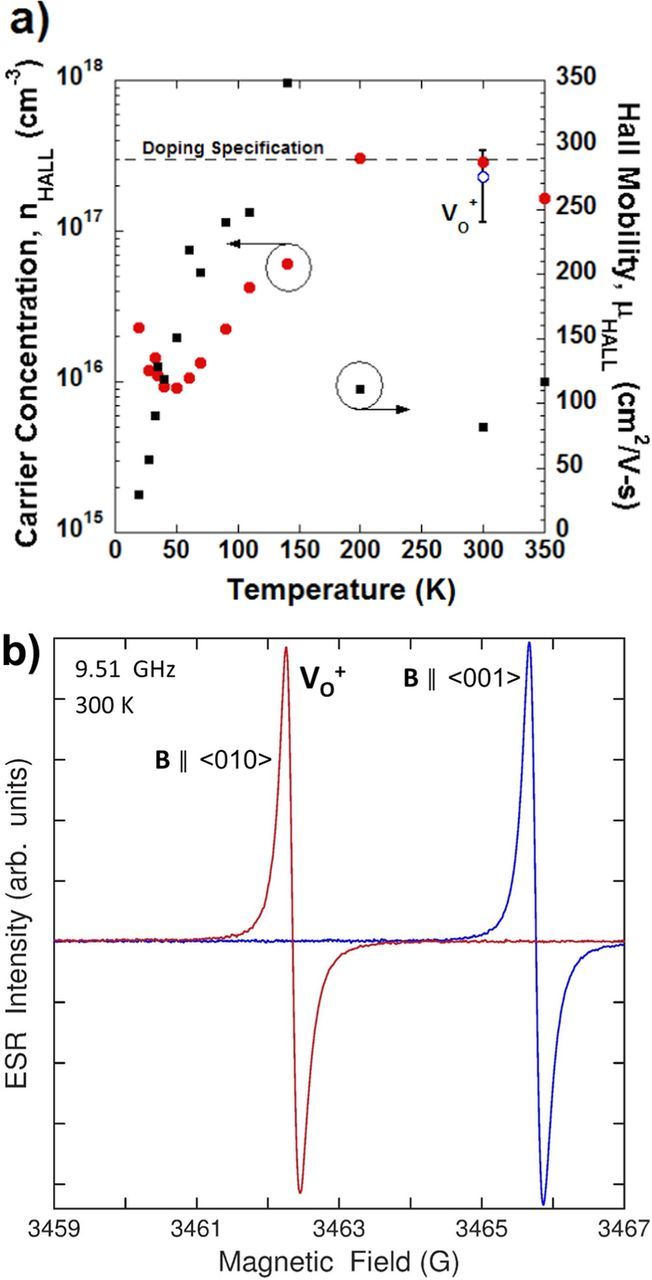
Figure 4. a) Temperature-dependent Hall measurement of carrier concentration and mobility for the (−201) Ga2O3 substrate. b) Electron spin resonance (ESR) spectra of (001) Ga2O3 with the magnetic field oriented parallel to the 〈010〉 and 〈001〉 directions.
In order to investigate the origin of electrons in the Ga2O3 substrate, electron spin resonance (ESR) was performed at room temperature on a 7.5 × 1 × 0.18 mm flake of (001) Ga2O3 cleaved from the (−201) substrate. The data is shown in Fig. 4b for the case when the magnetic field was parallel to the 〈010〉 and the 〈001〉 directions. The line width of about 0.2 G was similar to the one reported by Yamaga et al. for their undoped Ga2O3 bulk crystals.18 Our analysis yielded a density of oxygen vacancies (VO+) of 2.3 × 10¹⁷ (±50%) cm−3, indicating that other residual impurities in the substrate (e.g., Si) were not a major contributor to the unintentional doping of the substrate. While we have previously reported the presence of O vacancies in MOCVD-grown β-Ga2O3,19 here we note that their presence enabled transistor operation.
Summary
Initial results on an insulated-gate (001) β-Ga2O3 MOSFET with an ALD-grown HfO2 high-k gate dielectric were reported. A positive threshold voltage for a Ga2O3-based transistor was reported for the first time. Hall effect and ESR measurements indicated that the conductivity was due primarily to the presence of oxygen vacancies in the substrate. Capacitance-voltage and current-voltage measurements showed a positive threshold voltage at low drain bias. It remains to be confirmed that a high-k dielectric gated transistor fabricated on homoepitaxial Ga2O3 would yield an enhancement mode device. Further device performance improvements such as higher breakdown field and output current are expected by transitioning the process to homoepitaxial Sn-doped Ga2O3. A thorough understanding of the role of point defects such as oxygen vacancies in the donor activation and device performance remains to be developed.
Acknowledgments
The authors are sincerely grateful to Dr. Jeremy Robinson and Dr. Joshua Caldwell (NRL) for assistance with Ga2O3 exfoliation, Dr. Akito Kuramata (Novel Crystal Technology) for insightful discussions, and the NRL Nanoscience Institute staff ( Walter Spratt, Dean St. Amand) for fabrication equipment maintenance. Research at NRL was supported by the Office of Naval Research (ONR).