Abstract
Recent studies have shown superior thermal transport of graphene on copper as a potential candidate for the next generation interconnects. Using density function theory (DFT) we have studied the current transport of graphene/copper (G/Cu) hybrid-nano wire interconnect system and compared electrical characteristics with other two dimensional counterparts along with graphene. From the first principle calculation, band structure and density of states have been calculated. Using Landauer-Buttiker (LB) formalism, electrical transport is calculated. We explained why G/Cu hybrid interconnect shows more conductivity than graphene only interconnects with the help of phase space argument. As graphene on copper system has more available density of states near the Fermi level it offers more states than graphene for conduction.
Export citation and abstract BibTeX RIS

This is an open access article distributed under the terms of the Creative Commons Attribution Non-Commercial No Derivatives 4.0 License (CC BY-NC-ND, http://creativecommons.org/licenses/by-nc-nd/4.0/), which permits non-commercial reuse, distribution, and reproduction in any medium, provided the original work is not changed in any way and is properly cited. For permission for commercial reuse, please email: oa@electrochem.org.
In very large scale integration (VLSI), application of emerging nano-electronic devices demand compatible interconnect solution to meet challenges of ever-shrinking technology nodes. In scaled CMOS technology nodes, traditional copper based interconnect is facing challenges due to low scalability, electromigration, void formation, high resistivity and many other performance limitations.1 In search of emerging materials and for replacement of copper interconnect in nanometer CMOS technology nodes, graphene (G) and carbon nanotubes (CNT) have been studied intensively for a decade. Due to high electrothermal conductivities of different variants of carbon nanotube (CNT) and graphene, research has advanced further to explore potential of these nano-materials as future VLSI interconnect.2–12 Because of high thermal conductivity, CNT interconnects can quickly drain out heat to make interconnect more thermally stable.5,13 However, CNT wafer scale alignment in between contacts is still very challenging.14 Whether a CNT is metallic or not depends on chirality and that is why it requires separating CNT of particular chiralities from the growth media system. This selective growth and etching of CNT or separation of particular chirality remains an open challenge.15 Scalability of length is very crucial for interconnect technology from modeling and implementation perspective. In recent years, graphene nanoribbon (GNR) has received more attention due to ease of graphene (G) growth by chemical vapor deposition (CVD) and patterning using E-beam lithography. Although bulk two-dimensional graphene is semi-metallic with zero density of states at Dirac point, its one-dimensional counterpart GNR is not metallic always. As an interconnect material it is being sought to be metallic. As the width of GNR decreases bandgap opens up which makes this material not suitable for interconnect application. From chirality point of view, only zigzag edge (toward transport direction) is always metallic regardless of GNR width. On the other hand, armchair could be metallic or semiconducting depending on chirality. Therefore, metallic nature of GNR also becomes selective to chirality. Beside CNT and graphene, both of these materials share same challenge of contact resistance, which limits overall performance of interconnect significantly.16,17 This motivates scientific community to look for the hybrid material system to obtain metallic properties out of GNR while not losing greater thermal stability and mechanical strength. There is an ongoing research to find hybrid materials with better thermal and electrical conductivity.18
Recent studies found that graphene on copper might be a possible solution for lowering the temperature of interconnects.18,19 Reduction in peak temperature by 27% has been observed in graphene encapsulated copper wires.19 This reduction in temperature eventually reduces resistance and RC delay that increases data transfer by 15% from its copper nanoribbon counterpart. Previously graphene coated copper was reported for having excellent thermal property and attributed to copper nanoribbon not because of graphene.18 Graphene deposition on copper requires temperature around 1200 K while Cu annealing occurs and Cu grain size becomes larger. Larger grain of copper nanoribbon reduces resistivity by increasing electron's mean free path (MFP).20 In addition, graphene works as a barrier layer for a copper ion preventing diffusion into the dielectric. This is why it was believed that excellent electrical transport and thermal properties are inherent to copper; graphene is only assisting by providing a heat-spreading path to copper nanoribbon. Although internal dynamics requires more confirming experimental reports, it is also necessary to investigate this material system theoretically from the perspective of VLSI interconnect. Previously graphene growth dynamics21 and interfacial structure22 have been studied theoretically using first principle calculation. Using molecular dynamics (MD), thermal transport of graphene on copper has been also studied.23 However, for G/Cu system there is not much theoretical study from the point of view of electrical transport with a special focus on interconnects applications. In this work, we theoretically investigated G/Cu structure for bulk (2D) and for one-dimensional nanoribbon (1D) as a potential material for next generation interconnects applications.
In this work, we studied the band structure of G/Cu hybrid system and temperature dependent resistance of nano interconnects. We intend to understand theoretically how this hybrid material system outperforms graphene only interconnect at temperatures higher than the room temperature (RT). Here we calculated density of states (DOS), current-voltage relation (I-V) and resistance (R) of G/Cu nano ribbon interconnects at different temperatures to understand G/Cu system. From temperature dependent resistance we calculated temperature coefficient of resistivity (TCR) and found it to be constant at low biases. This introduction is followed by a section on methods of calculations. We have presented results and discussion in the subsequent section. At the end, we have addressed future prospects and limitations of this work.
Simulation Methods
We considered three atomic layers of copper arranged in such a way that ⟨111⟩ crystal plane is aligned toward Z-axis. Therefore, flat surface of copper is ⟨111⟩ plane. On top of this flat surface of copper, we placed graphene monolayer. Graphene monolayer was placed in such a way that graphene edge is zigzag toward the transport direction, which is X-axis in this case. Since Cu {111} plane is a hexagonal lattice with almost similar lattice constant like graphene (2% mismatch), we have placed graphene atoms on {111} planes of Cu. Unit cell of bulk two-dimensional G/Cu system consists of three copper atoms in three different atomic layers along with two carbon atoms sitting on the top most copper layer. Lattice constant and lattice vectors are shown in Figure 1. For electrical transport studies, we considered one-dimensional hybrid G/Cu nanoribbon of width 0.6 nm, height 0.8 nm. For a finite length, we limited our atomistic simulation up to 10 nm of interconnect length.
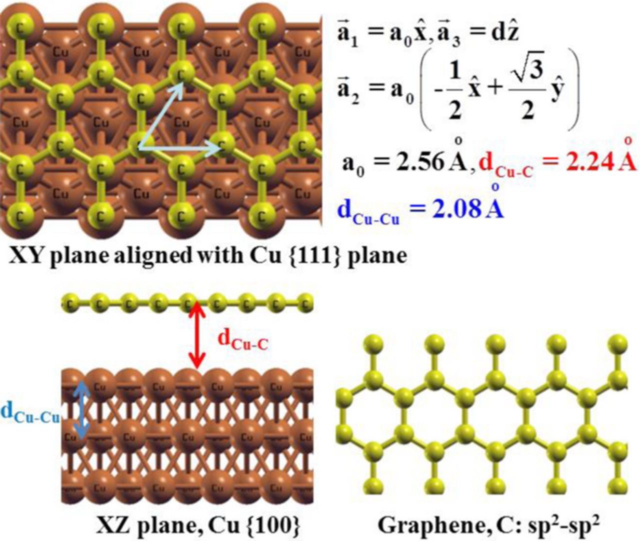
Figure 1. Atomic structure of graphene on copper hybrid nano-interconnect in XY plane (top) and in XZ plane (bottom). Cu {111} plane is toward Cartesian Z-axis (which is XY plane). Lattice vectors for this system are shown on top right. Scale for the top, bottom and bottom-right are not same.
We used density functional theory (DFT) to study electronic band structure within Quantum-Espresso (QE) code.24 For exchange correlation (XC) we used local density approximation (LDA) specifically developed by Perdew-Zunger.25 Projector augmented-wave26 type pseudo-potentials which were used to obtain relativistic correction and also to consider contribution of core electrons. For atomic structure optimization, we used fixed cell relaxation calculation. We performed relaxation calculation by fixing bottom layer of Cu atoms in their bulk position as the reference plane. In relaxation calculation, atoms in top two Cu layers and graphene layer were allowed to move in finding minimum energy position for the whole system in equilibrium. We started relaxation calculation with atomic positions calculated from their bulk system. Later on we used updated atomic positions obtained from the relaxation calculation. Inter-planar distance for Cu {111} planes is 2.08 Å, which is calculated from the bulk copper lattice constant in ⟨100⟩ plane (3.6149 Å). The distance between top Cu layer and graphene layer is 2.24 Å.22 We began relaxation calculation with lattice constant 2.56Å and obtained atomic positions of top two layers (two layers of Cu and one layer of graphene) by minimizing force up to 0.05 eV·Å−1. Because of relaxation, we found that C-Cu interlayer distance increases slightly. Relaxation calculation optimizes co-ordinates for all atoms in the system for finding the minimum energy state. From our calculation of an optimized structure, we found that three atomic layers of copper can best describe the properties under study. It is for this reason we have limited our study to 3-layers of copper only. Using these optimized atomic positions, we then performed self-consistent field (SCF) calculation.
In each SCF cycle, it calculates electron density field. Using variational method, this SCF calculation is a minimization technique for electron density function. It tries to minimize overall system energy for a particular electron density distribution. When the difference of system total energies of two consecutive SCF cycles reached as small as 10−9 eV we stop SCF calculation. SCF calculation took 41 iterations to converge with a tolerance of 10−9 eV. In SCF calculation, energy cut off 40 Rydberg (Ry) was used to limit wave functions tails. During SCF calculation, we sampled Brillouin Zone (BZ) uniformly with 32 × 32 × 1 K-grids using Monkhorst-Pack (MP) method27 for 2D bulk system. For one-dimensional nanoribbon, we used 128 × 1 × 1 K-grids. MP method ensures generation of special points in the BZ for facilitating efficient integration of periodic functions of the wave vector over entire BZ. Total overall system energy from SCF calculation was −1977Ry for a one-dimensional system and −658Ry for a 2D bulk system. Total energy for 2D bulk is for five atoms basis while for nanoribbon number of atoms is fifteen. That is why total system energy is higher in nanoribbon case. Electron density obtained from SCF calculation was used for another round of calculation for finding energy levels for each point of a densely sampled BZ. We used 64 × 64 × 1 k-grids for BZ sampling using the MP method for 2D bulk and 256 × 1 × 1 for nanoribbon. From this calculation, we obtained electronic band structure and electrons occupations in those energy states. We performed band structure calculation for 80 energy levels and obtained 0.7179 eV Fermi energy for the bulk case and −3.9858 eV for the hybrid nanoribbon. Later on for all other calculations, we adjusted these Fermi energies to 0 eV when necessary for comparison or for transport calculations. From SCF calculation, we constructed band structures and calculated density of states (DOS) of this hybrid system within QE code. For DOS calculation, energy levels are adjusted in such way that the Fermi energy becomes 0 eV. Energy spectrum is sampled with a resolution of 10 meV.
We used Wannier90 code28 for transport study based on the Bloch states obtained from SCF calculations. First step is to transform Bloch waves into Wannier Function and then finding maximally localized Wannier Wave Function (MLWF). Rest of transport properties depend on MLWF. From MLWF we computed current voltage relation (I-V). Since the length of this interconnect is very short, we had to decide the right theory for transport. Typical electronic MFP of copper is 40 nm and few microns for graphene. We assumed for this hybrid system electron's MFP to be greater than 40 nm and smaller than 1000 nm. If this is the case for the MFP then this hybrid interconnect transport should be ballistic in nature for any given interconnect length less than 40 nm. Hence, to compute current-voltage relation at different temperatures we adopted Landauer-Buttiker (LB) formalism implemented in Wannier90 code,28
![Equation ([1])](https://content.cld.iop.org/journals/2162-8777/6/4/P119/revision1/d0001.gif)
Here e is electronic charge and h is Planck constant. M counts the number of transport modes for a conductor, μ1 and μ2 are electrochemical potentials of left and right contacts. Wannier90 code uses Bloch States obtained from QE code to obtain MLWF and construct system Hamiltonian. After obtaining Hamiltonian, Wannier90 uses Non-equilibrium Green Function (NEGF) for the transport calculation and transmission coefficient. In Landauer formalism, by definition the transmission coefficient is QC. Due to high computational cost for first principle study, we have limited our study to a 10 nm long wire, which represents a short local interconnect and a good example of ballistic transport. For ballistic transport, one should not use Fuchs-Sondheimer (FS) and Mavadas-Shatzkes (MS) models20 for resistivity estimation. Therefore, in ballistic transport regime, instead of FS and MS theories we have used LB formalism. In NEGF method, temperature variation was taken into account by manipulating value of thermal broadening (∼3.5KBT). From current voltage characteristics at different temperatures, we have calculated temperature dependent resistance. We use the following equation for TCR calculation,
![Equation ([2])](https://content.cld.iop.org/journals/2162-8777/6/4/P119/revision1/d0002.gif)
where α is TCR at 300 K and R0 is resistance at 300 K.
Results and Discussion
Electronic band structure of G/Cu hybrid system for bulk (2-D) and nanoribbon (1-D) are showed in Figures 2 and 3 respectively. From band structure of bulk 2D system, it is apparent that four bands are crossing Fermi level (0.7179 eV). Those Fermi level crossing bands are highlighted with red, green, blue and orange color in Figure 2a in the order of their energy from low to high energy. We counted band index from the lowest energy one as first (near −15 eV). With this counting, bands with indexes 20 to 23 are contributing in constructing the Fermi surface. For a metallic system, this multiple band crossing is expected. DOS of G/Cu bulk system is shown in Figure 2b. Being an infinite two-dimensional system, DOS is continuous. Most importantly DOS is continuous and non-zero near the Fermi energy. Just below 0 eV, there is a dense crowd of bands that is consistent in DOS also.
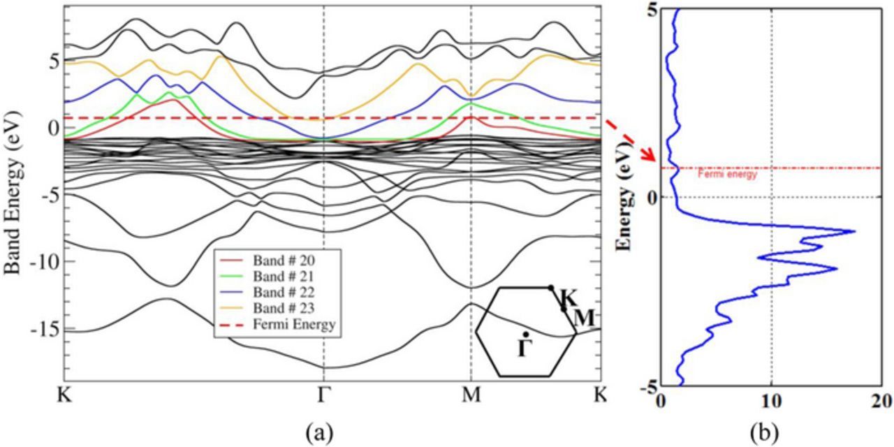
Figure 2. (a) Band structure of G/Cu bulk system. Bands contributing to contstruct Fermi surface are high lighted with color. Fermi Energy is 0.7179 eV shown in red dashed line. At the bottom left corner of the band strucuture plot BZ speical points are shown. (b) Density of States (DOS) from −5 eV to 5 eV are shown. Fermi energy is marked in DOS plot seperately with red dashed line. Unit of bulk DOS is states/eV/atom.
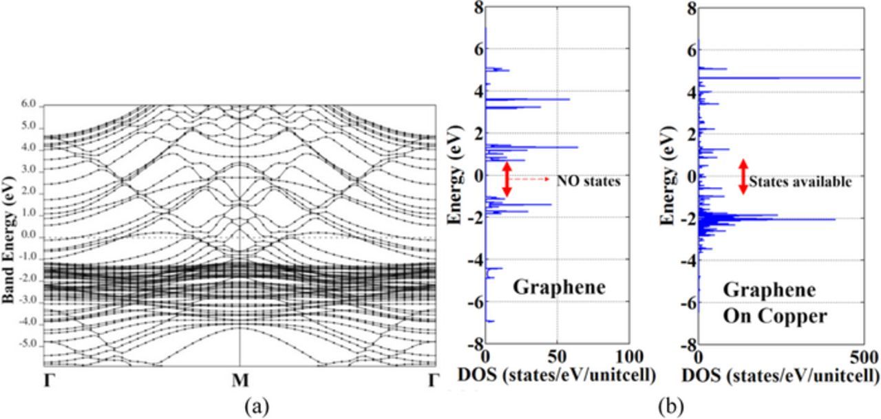
Figure 3. (a) Electronic band structure of G/Cu nanoribbon. Fermi level at −4.08 eV (b) Density of states of graphene interconnect are compared with graphene/copper interconnect. Fermi energy is set to 0 eV in (a) and (b) for the purpose of comparison of two different material systems. Near the Fermi energy, there are no states available for the graphene interconnect.
For G/Cu nanoribbon, band structure and DOS are shown in Figures 3a and 3b, respectively. Unlike GNR, there is a non-zero DOS at Fermi level for G/Cu nanoribbon. In case of nanoribbon, DOS is discrete due to one-dimensional confinement of the electron. In this hybrid system because of Cu, more states are available in an energy window near the Fermi energy. Figure 3b shows the density of states (DOS) comparison of graphene and G/Cu material system. This difference of DOS in these two material systems causes their difference in current transport. Density of states near the Fermi energy do not change significantly with increasing the number of copper layers. Increasing the number of copper layers will increase absolute number of DOS and charge carriers as well as the electrical conductance. However, the electrical conductivity which depends on per unit volume does not change because as we increase number of copper layers we are also increasing a total volume. Therefore, near the Fermi energy, three layers of copper best describe the structure which is computationally less expensive than a structure with the higher number of copper layers. According to transport theory, if there are no available electronic states in the transport media for a given energy window, no transport will happen for electrons of that particular energy window. In Figure 4a, graphene current-voltage relation has been compared with G/Cu system. For any biasing voltages, in between −1.34 V and 1.34 V, I-V curve is flat for graphene and linear for G/Cu system.
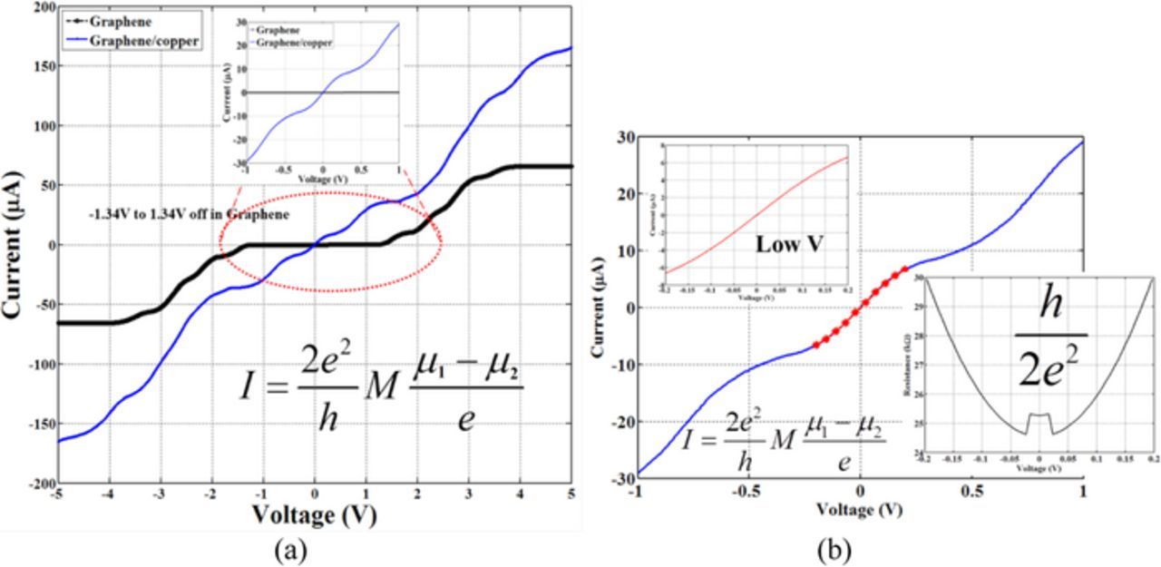
Figure 4. (a) Current voltage (I-V) characteristics of G/Cu nanoribbon interconnect compared with graphene only interconnect. For graphene, no current is observed between −1.34 V to 1.34 V because of not having available states in that energy window. However, graphene on copper is still conductive in this window. (b) I-V characteristics of G/Cu with lower bias voltage. Top inset shows linear region near zero bias and lower inset shows resistance versus voltage relations.
In the energy window −1.34 eV to 1.34 eV, there is no electronic transport for graphene. However, for G/Cu there is electronic conduction in a broad energy window because of availability of electronic states as shown in Figure 3b. This is why at low biasing G/Cu is a better conductor than graphene nanoribbon. Because of quantum confinement, graphene nanoribbon behaves like a semiconductor rather than a conductor.
In Figure 5, current versus voltage (I-V) characteristics are shown at different temperatures. This will be further confirmed by low TCR values for this interconnect material system. Plateaus are showed in inset of Figure 4. Due to lateral confinement, energy levels are discrete and so is QC spectra as in quantum well. Due to discrete QC, these plateaus are observable. I-V characteristics of Figure 5 have been used to compute resistance versus current at different temperatures in Figure 6. Slope of I-V curve changes near a plateau and ends up with oscillation in resistance. We have shown temperature dependent resistance in Figure 6 for low bias current. Resistance increases with the temperature, which is expected for positive TCR materials. This is in contrast to graphene interconnect case where resistance quenching happens at high temperatures.29 Interestingly, resistance decreases with increase of biasing current. This is due to plateau as mentioned earlier. At 300 K, the resistivity of the hybrid structure is calculated as 125 μΩ-cm whereas Cu bulk resistivity is 1.72 μΩ-cm.30 As estimated by the MS-FS theory,20 MPF of Cu will decrease for width below 40 nm which will increase wire resistivity significantly. Experimentally 180 nm G/Cu nanowire has been tested and measured resistivity is 5 μΩ-cm which is in good agreement with MS-FS theory.20 Bellow 180 nm, G/Cu nanowire structure is yet to be measured experimentally.
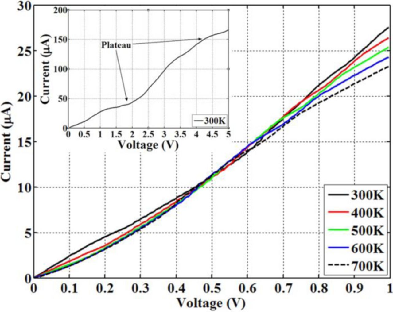
Figure 5. I-V characteristics of G/Cu interconnect at different temperatures. Inset shows I-V characteristics for 0 to 5 V bias with several plateaus.
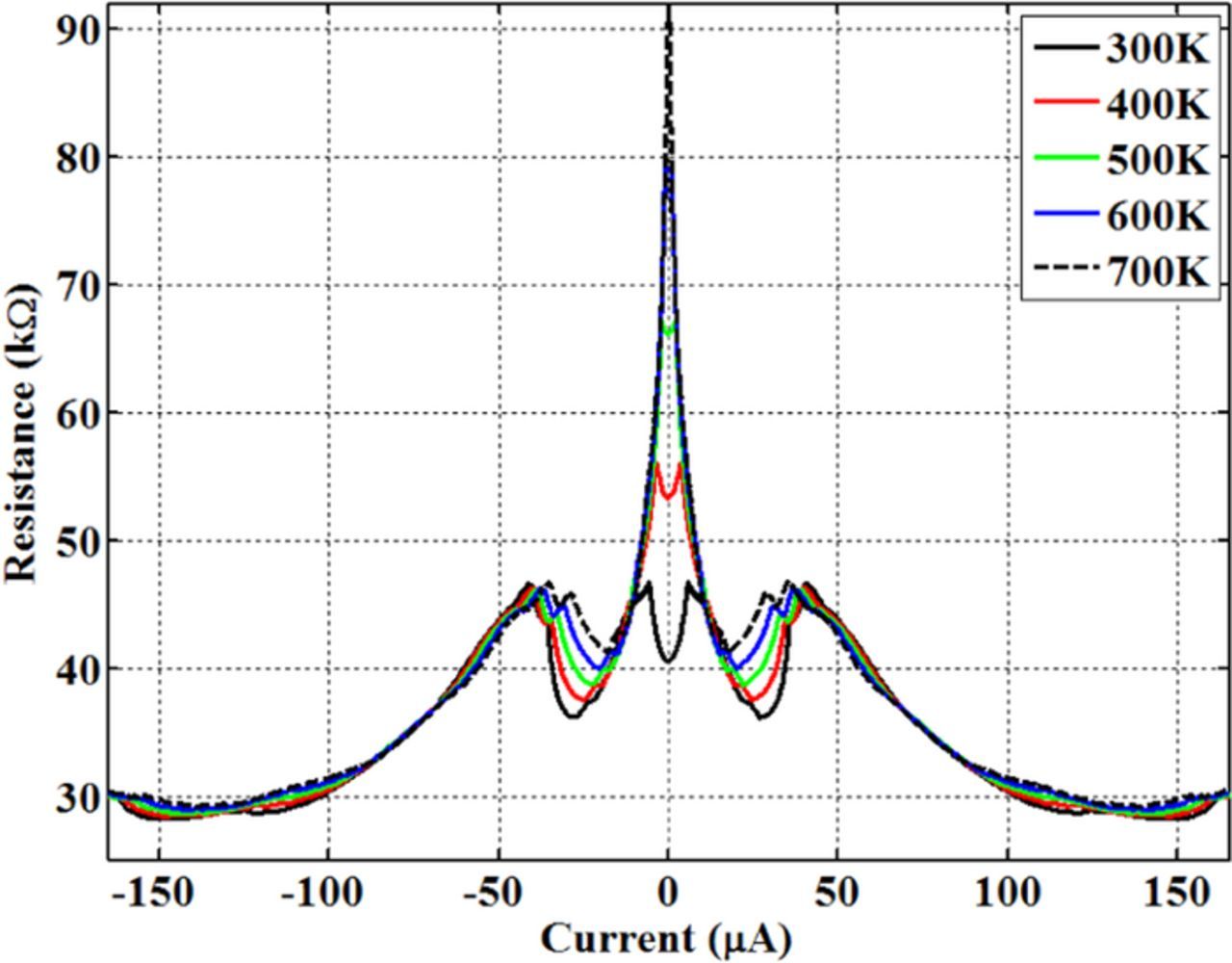
Figure 6. Resistance versus current at different temperatures.
In Figure 7, it was shown that the resistance increases up to 6 μA and then starts decreasing. Since in higher energies far from the Fermi level there is more DOS hence denser QC brings the resistance down. Figure 8 shows how resistance varies at different current bias at room temperature. Figure 9 shows the differential resistance. There is a sharp jump in differential resistance around 48 μA. It is also apparent in Figure 6 that around 48 μA resistance begins to oscillate. Again beyond 48 μA resistance decreases monotonically. In Figure 10, temperature dependent resistances are shown at different bias voltages. We limit bias voltage from few tens of mV to 200mV keeping in mind that next generation low power interconnect will not suffer that high bias stress. On the other hand interconnect might suffer from high current stress but not voltage stress. It is apparent that in all biasing voltages, resistance increases linearly with the temperature at least around normal semiconductor operational range (300 to 370 K). This infers to have constant positive TCR which we present in Figure 11. At 50mV bias, calculated TCR is 0.00315 K−1 which is lower than the bulk TCR values of other commonly used interconnect materials. For instance, at 300 K TCR for bulk copper, silver and aluminum are 0.00386 K−1, 0.0038 K−1, and 0.00429 K−1, respectively. If we estimate TCR for nanoribbon of these materials, it would be more than their bulk values because of size effect. Therefore, we can expect that this G/Cu nanoribbon interconnect will be having less TCR than any pure metallic nanoribbon made of any known metal of interest. Low values of TCR indicate that resistance in this G/Cu hybrid system is less sensitive to temperature fluctuation in the chip. Due to self-heating, there are always several high activity regions in the chip, which are called hot spots. Near the hot spot, temperature is elevated over the normal chip operating temperature. An interconnect with high TCR will not be a suitable choice because of its sensitivity to temperature. It is important to have a uniform clock pulse and uniform RC delay across the chip. To have uniform RC delay, resistance needs to be less sensitive to temperature variation. Interestingly, G/Cu shows negative slope of TCR with increase of bias voltage and it is due to plateau behavior in I-V characteristics.
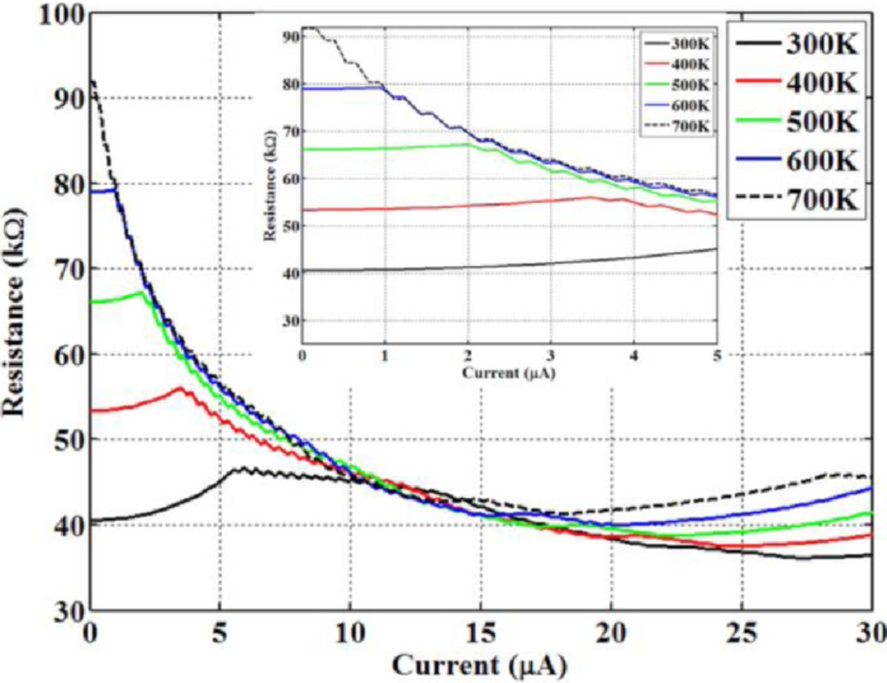
Figure 7. Resistance versus current at low bias current.
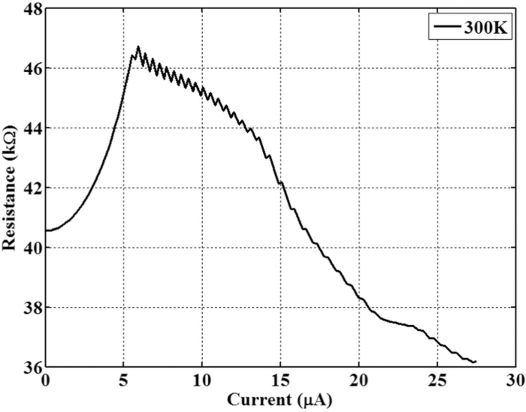
Figure 8. Resistance versus current variation at room temperature. Resistance decreases with increase in biasing current due to plateau in I-V characteristics.
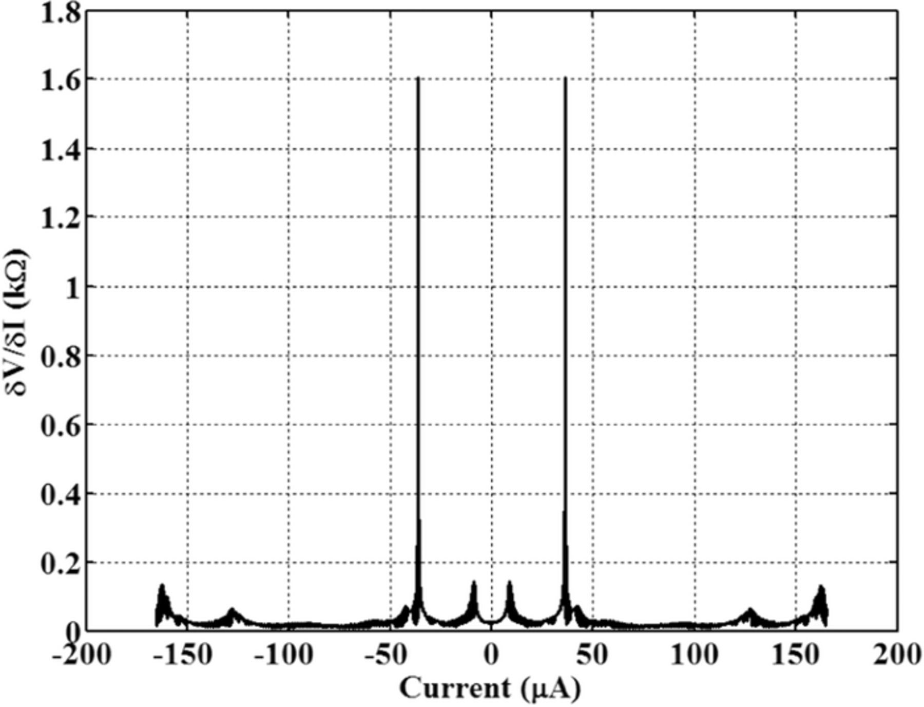
Figure 9. Differential resistance versus current.
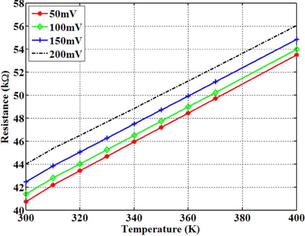
Figure 10. Temperature dependent resistance at different bias voltages.
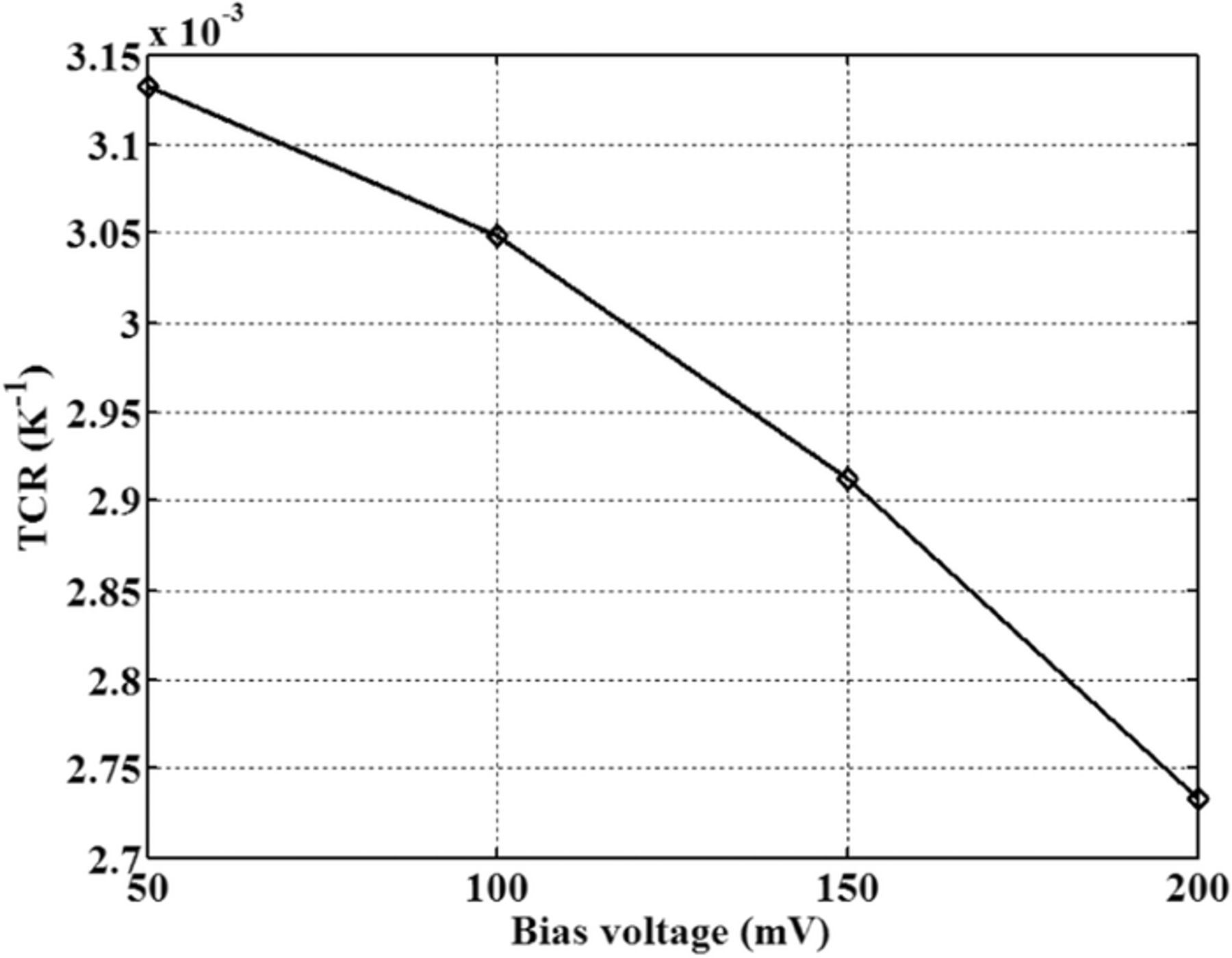
Figure 11. Temperature coefficient of resistance change with bias voltage.
Conclusions
We have simulated a graphene on copper nano-interconnect using DFT code. In addition to I-V characteristics, we studied temperature dependent electrical resistivity and temperature coefficient of resistance (TCR). Calculated TCR at room temperature is found to be lower than the commonly used other metals such as copper and aluminum. Several plateaus in I-V characteristics are observed for this hybrid interconnect system. The hybrid structure shows better conductivity at low bias than graphene only interconnect. Graphene only nanoribbon might perform better for the device but not for interconnect. Further study is needed in understanding of frequency response characteristics, reliability and integration with the existing CMOS technology. The work can be used in advancing an understanding of electrical performances of other nanostructures for possible interconnect materials.
Acknowledgments
Part of the work is supported by the United States Air Force Research Laboratory under agreement number FA9453‐10‐1‐0002. The U. S. Government is authorized to reproduce and distribute reprints for Government purposes notwithstanding any copyright notation thereon.