
Abstract
Boron carbon nitride (BCN) thin films were deposited by a dual target DC and RF sputtering technique. The films were deposited using various combinations of nitrogen and argon working gases and B4C, BN, and C targets. X-ray photoelectron spectroscopy and Fourier-transform infra-red spectroscopy were utilized, respectively, to investigate the changes in chemical composition and bonding that occurred for films deposited under various N2/Ar gas flow ratios and DC/RF target powers. The composition and bonding were correlated to separate measurements of the BCN mass density, dielectric constant, Young's modulus, and hardness. All BCN films were observed to have relatively low mass densities ranging from 2.0–2.5 g/cm3. BN rich BCN films were observed to be insulating with relatively low dielectric constants of 3.9–4.6 and Young's modulus and hardness values of 110–150 GPa and 5–13 GPa, respectively. BC rich BCN films were observed to be comparatively leaky dielectrics but did exhibit extreme mechanical properties with Young's modulus and hardness values exceeding in some cases 300 GPa and 30 GPa, respectively.
Export citation and abstract BibTeX RIS

This is an open access article distributed under the terms of the Creative Commons Attribution 4.0 License (CC BY, http://creativecommons.org/licenses/by/4.0/), which permits unrestricted reuse of the work in any medium, provided the original work is properly cited.
Nanoelectronic metal interconnects have many unique nanoscale electrical, thermal, and mechanical challenges.1–3 While dimensional scaling has produced tremendous improvements in transistor performance,4 it has produced an opposite effect on the associated metal interconnect leading to increased critical path signal delays and possible degradation of the overall integrated circuit performance.5 As the interconnect signal delays are proportional both to the resistance of the interconnect metal and the capacitance of the insulating interlayer dielectric (ILD), new materials with reduced values of resistivity and dielectric permittivity have been sought to mitigate the negative effects of dimensional scaling.5 Since relatively few materials exhibit a lower resistivity compared to the currently utilized interconnect metal copper (Cu), most materials based interconnect delay reduction efforts have focused on implementing new ILD materials with increasingly lower values of dielectric constant (i.e. low-k).6 Unfortunately, the hybrid inorganic-organic silicate (a-SiOC:H) materials currently utilized as low-k ILDs exhibit reduced electrical, thermal and mechanical properties in addition to reduced values of dielectric permittivity.5–7 These overall reduced properties have severely aggravated a variety of interconnect related reliability issues such as time dependent dielectric breakdown and die cracking during packaging.2,3
Compounds in the boron-carbon-nitrogen phase diagram (such as diamond (C), cubic boron nitride (c-BN), and boron carbide (B4C)) are potentially attractive as alternative low-k dielectric materials due to their covalent bonding, short bond lengths, and low atomic mass that leads to a unique combination of low dielectric constant but high thermal and mechanical strength.8–12 Some of the already prominently reported properties for these materials include good wear resistance, high hardness, and low coefficient of friction. These excellent properties have made BCN materials frontrunners for hard and protective coatings in cutting tools and other anti-wear applications.13,14 From a low-k interconnect perspective, amorphous hydrogenated BN (a-BN:H) has been previously demonstrated as a low-k dielectric with k a of ∼ 4.0–5.7.15–17 However due to a hygroscopic nature, a-BN:H has exhibited a variety of thin film delamination issues that have limited its implementation.18,19 In this respect, carbon can be added to the BN structure to produce boron carbon nitride (BCN) films with potentially reduced moisture sensitivity, but with hardness values still as high as 20 GPa.20 The incorporation of carbon as terminal organic groups can also lead to even lower values of dielectric constant with values as low as 1.9–2.1 reported for some plasma enhanced chemically vapor deposited (PECVD) BCN thin films.21–23 PECVD BCN films have also shown the ability to suppress Cu migration and diffusion which is an additional important consideration for low-k metal interconnect applications.23 Thus BCN compounds offer the potential to combine the excellent properties of diamond, c-BN, and B4C with their exact properties adaptable depending on their composition and structure.24–26
Beyond PECVD, several other methods for depositing BCN thin films have been reported in the literature including: chemical vapor deposition (CVD),27,28 pulsed laser ablation,29 ion beam assisted deposition,30 and DC/RF magnetron sputtering.31,32 In this study, we have chosen to investigate amorphous BCN films deposited via dual target sputtering. The sputtering technique provides unique advantages over other techniques such as freedom to choose the substrate material and uniform deposition over a relatively large area. Furthermore, the dual target approach allows better control of the deposition parameters to prepare BCN films of varying composition. The ability to control composition has allowed us to investigate the role this plays on the dielectric and mechanical properties of BCN materials for both low-k dielectric and anti-wear/protective coating applications. We show that the composition and structure of these materials can cause the dielectric and mechanical properties of BCN to vary dramatically with dielectric properties ranging from insulating to leaky and Young's modulus and hardness ranging from 100–300 and 10–30 GPa, respectively.
Experimental
Boron carbon nitride (BCN) films were prepared by dual target sputtering using two different sets of targets with different DC and RF biases. The first set of experiments were performed with a DC biased carbon target in combination with an RF biased BN target. The second set of experiments utilized a DC biased B4C target with the RF biased BN target. All sputter targets utilized were three inch in diameter. Nitrogen diluted in argon was used as a reactive sputtering gas and additional source of nitrogen. A base pressure of ∼ 4 × 10⁻⁷ Torr was achieved using a turbo molecular pump. The pressure during sputtering was maintained at 4 mTorr for all depositions. The substrate temperature used during deposition was room temperature in all cases. The percentage nitrogen added to the argon gas flow (N2/Ar+N2) were varied from 0 to 1 in increments 0.1–0.2. In other depositions the N2/Ar ratio was fixed while the DC or RF power was increased from 100 to 200W with the other kept constant at 100 W. These parameters were used to study the composition and resulting variation in Young's modulus and hardness variation.
The BCN films were deposited on a pre-cleaned oxidized silicon substrate. The thickness of the investigated films was in the range of 200–400 nm as determined by stylus profilometry of uncoated portions of the substrate and verified by separate optical ellipsometric measurements. The mass density (ρ) of the films was measured by X-ray reflectivity (XRR) using a Siemens D5000 equipped with a Cu line source and graphite monochromator. The data was collected in the range of 0 to 9000–15,000 arc sec with approximately 20 arc sec steps. The XRR spectra were fitted using the REFS software package (version 4.0, Bede). For the simulations, the thickness was fixed at the value determined by ellipsometry and the mass density was adjusted to fit the XRR spectra.33
X-ray photoelectron spectroscopy (XPS) was utilized to determine the nominal elemental composition and Fourier transform-infrared (FTIR) spectroscopy to investigate the chemical bonding of the BCN films. The XPS measurements were performed after ex-situ transfer to a VG Theta 300 XPS system having a hemispherical analyzer and a monochromated Al anode X-ray source (1486.6 eV).34 Removal of ex-situ surface contamination and depth profiling was achieved using a 2 keV Ar+ ion sputtering beam. A pass energy of 20 eV was utilized for collecting high resolution scans of the B1s, N1s, C1s, and O1s core levels as the Ar+ beam sputtered through a portion of the film.16 Bulk elemental concentrations were determined from these spectra via integrating the peak area and normalizing using appropriate calibration factors. FTIR measurements were performed in both transmission and reflection mode. The transmission FTIR measurements were performed with a Nicolet-Magna-IR 860 spectrometer.35 The reflection FTIR measurements were performed with the same spectrometer in combination with a Ge attenuated reflection (ATR) cell from Harrick Scientific.36 Both transmission and reflection FTIR spectra were collected from 400–4000 cm−1 with a resolution of 4 cm−1.
The dielectric properties of the BCN films were investigated via low frequency (100 kHz) capacitance-voltage (CV) measurements performed with a Hg prober.37 The dielectric constant of the films was determined by measuring the capacitance of the metal-insulator-semiconductor when sweeping the semiconducting Si substrate into accumulation and using the elementary parallel plate capacitor equation and the film thickness to calculate k. The area of the Hg probe contact was calibrated by measuring the capacitance for a thermal oxide of known thickness and k (= 3.9).38
Nanoindentation tests were performed with a Hysitron Triboindenter and a Berkovich diamond tip with a load range of 4 mN.39 Each sample was tested at ten locations. Depth-dependent properties were collected by performing multiple load/unload cycles. At different indentation loads, hardness (H) and indentation modulus (I) were calculated. Young's modulus was then calculated assuming a Poisson's ratio of 0.25 and using the depth-dependent apparent modulus via linear extrapolation.40
Results and Discussion
BCN FTIR and XPS analysis
Table I summarizes the XPS data for a series of BCN films deposited at room temperature using various N2/Ar ratios and the C and BN targets. For all films, XPS detected the presence of B, C, N and some oxygen (O) contamination (typically < 3%). The latter is attributed to background H2O, CO, and CO2 in the high vacuum sputtering system. Carbon nitride rich (> 95%) BCN films were obtained when sputtering with Ar gas only. However, the B content increased significantly from < 5% to ∼ 34% with the addition of just 20% N2. The B, C, and N content remained relatively fixed at ∼ 34, 18, and 45%, respectively with increasing percentage of N2 working gas.41
Table I. XPS elemental composition, mass density, and dielectric constant for BCN thin films sputter deposited using C and BN targets and different N2/Ar gas flow ratios. NM = not measured due to high leakage currents.
| ρ | |||||||
|---|---|---|---|---|---|---|---|
| % N2 | % Ar | % B | % C | % N | % O | (g/cm3) | k |
| 0% | 100% | 1.7 | 18.5 | 78.5 | 1.3 | 2.4±0.1 | NM |
| 22% | 78% | 34.2 | 18.9 | 45 | 1.9 | 2.1±0.1 | NM |
| 33% | 67% | 34.5 | 19.1 | 44.9 | 1.5 | 2.0±0.1 | NM |
| 50% | 50% | 34.5 | 16.6 | 46 | 2.9 | 2.1±0.1 | 4.3±0.1 |
| 70% | 30% | 29.1 | 14.8 | 46.2 | 9.9 | 2.0±0.1 | NM |
| 100% | 0% | 34.4 | 18.8 | 44.7 | 2 | 2.0±0.1 | 5.0±0.1 |
Figure 1 shows transmission FTIR spectra for the same set of BCN films discussed above. For the film deposited using only Ar, a single broad peak centered at ∼ 1150 cm−1 was observed and is attributed to a C-C or C-N vibration mode based on the XPS composition. For the other BCN films, three distinct peaks were observed in the FTIR spectra. The strongest peak centered at approximately 1400 cm−1 is fairly broad and extends over the range of 1100 to 1700 cm−1. The other two smaller peaks were centered at ∼ 800 and 2200 cm−1. The peaks at 1400 cm−1 and 800 cm−1 are typically attributed to the in-plane stretching and out-of-plane bending vibrations of sp2 bonded h-BN.42–44 Broadening of these two bands could be due to the incorporation of C into the h-BN structure to form BCN.32 The absorption bands for C-N, C=N, C≡N bonds are typically located at 1300, 1600 and 2170 cm−1, respectively.45–47 Therefore the extension of the band from 1300 to 1600 cm−1 suggests the formation of the C-N and/or C=N bonds in addition to sp2 B-N bonds.48,49 However, there is no peak splitting in the band which confirms that there is no separate BN and CN phases in the film. The slight shifting of the 800 and 1400 cm−1 peaks to higher wavenumbers and increased absorbance with higher N2/Ar ratios likely indicates that a BN rich BCN film is more favorably formed at higher N2/Ar gas ratios. Therefore, the atomic arrangement and short range order is probably h-BN like, but with some sp2 B-N bonds being replaced by sp2 C-N and C=N bonds to give a sp2-BCN phase.
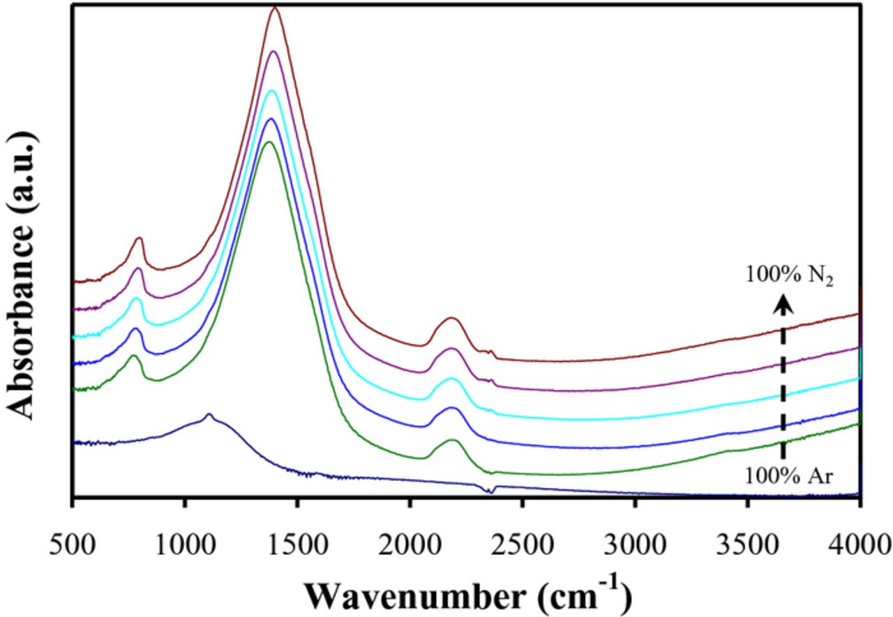
Figure 1. FTIR spectra for BCN films sputter deposited at room temperature using C and BN targets and various N2/Ar gas ratios.
The peak at ∼ 2170 cm−1 in Figure 1 could be attributed to either C≡N or B-H bonding. The latter is typically observed at wavenumbers of ∼2500 cm−1 for the B-H stretching mode and ∼ 2000 cm−1 for the bridging B-H-B absorption band.36 As < 1% hydrogen was detected in separate combined Rutherford backscattering and nuclear reaction analysis measurements, the peak at 2170 cm−1 is therefore attributed C≡N. This is consistent with the prior assertion of the presence of some C-N and C=N bonding as well.
Table II summarizes the XPS data for a series of BCN films deposited at room temperature using various N2/Ar ratios and the B4C and BN targets. In this case, films deposited with pure Ar were found to be B rich with <10% C and N. However, the N content increased significantly from <5% to ∼ 33% with the addition of just 20% N2. The N content increased to a maximum value of 37% with the addition of 40% N2 before decreasing back to 25% for sputtering in pure N2. As indicated in Table II, the decrease in N content is likely due to the incorporation of higher levels of oxygen contaminants (10–20%) in these specific BCN films. Interestingly, the carbon content remained relatively fixed at 9–14% for all Ar and N2 gas combinations.
Table II. XPS elemental composition, mass density, and dielectric constant for BCN thin films sputter deposited using B4C and BN targets and different N2/Ar gas flow ratios.
| ρ | |||||||
|---|---|---|---|---|---|---|---|
| % N2 | % Ar | % B | % C | % N | % O | (g/cm3) | k |
| 0% | 100% | 78.8 | 8.9 | 5.2 | 7.2 | 2.5±0.1 | NM |
| 20% | 80% | 46.5 | 10.1 | 32.9 | 10.5 | 2.1±0.1 | 3.9±0.1 |
| 33% | 67% | 45.5 | 14.4 | 37.4 | 2.7 | 2.1±0.1 | 4.5±0.1 |
| 40% | 60% | 45.5 | 14.4 | 37.4 | 2.7 | 2.0±0.1 | 3.9±0.1 |
| 50% | 50% | 46.1 | 11.6 | 32.8 | 9.6 | 2.1±0.1 | 4.6±0.1 |
| 100% | 0% | 44.7 | 10.6 | 24.7 | 20.0 | 2.2±0.1 | 4.3±0.1 |
Figure 2 shows a reflection Ge ATR-FTIR spectra for the same set of BCN films sputter deposited using the B4C and BN targets. For the film deposited using only Ar, a single broad peak centered at ∼ 1100 cm−1 was observed. This band is attributed to B-B inter and intra-icosahedral vibrational modes consistent with the large B composition determined by XPS.36,50 A faint absorption band at ∼ 2500 cm−1 is also observed and attributed to the B-H stretching mode (again consistent with the B rich composition).36 With addition of N2 sputtering gas, the 1100 cm−1 absorption band shifted to 1400 cm−1 consistent with the T-FTIR spectra collected for the C/BN sputtered films. Due to the similarities, we similarly attribute this peak to mixed sp2 BN and CN stretching modes. The intensity of this band increases with increasing% N2 working gas and then decreases for 100% N2. This is consistent with the XPS measurements where the N content was observed to increase and then decrease with increasing% N2.
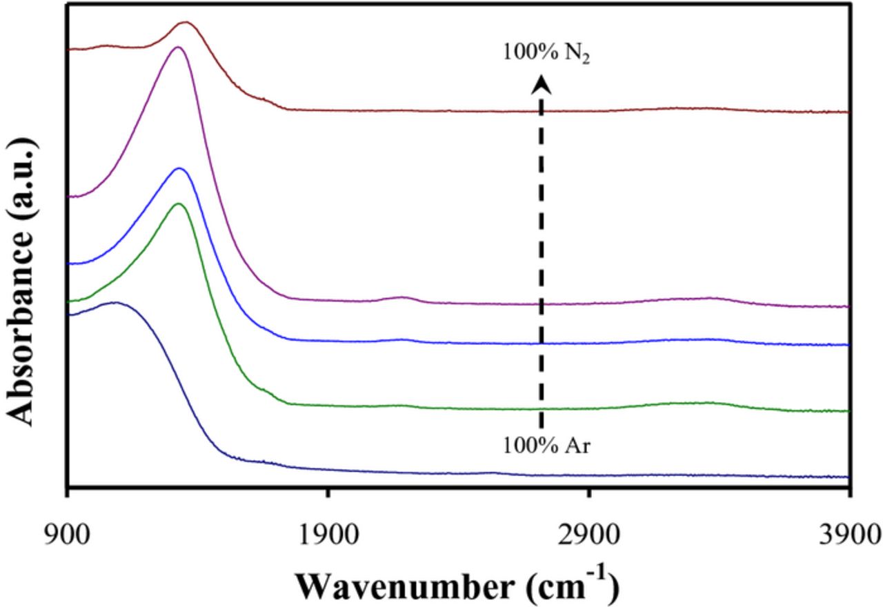
Figure 2. FTIR spectra for BCN films sputter deposited at room temperature using B4C and BN targets and various N2/Ar gas ratios.
In Figure 2, small peaks at 2200 and 3350 cm−1 are also observed. The former has been previously attributed to C≡N bonding. The latter is attributed to N-H bonding consistent with prior observations of PECVD a-BN:H films. This suggests the presence of a significant amount of hydrogen (∼ 10–15%) for the B4C/BN sputter deposited films. Interestingly, the C≡N and N-H peaks largely disappear for the 100% N2 sputter deposited film.
Table III summarizes the XPS data for DC and RF power skews performed with the B4C and BN targets. The% N2 working gas was intentionally set low at 10% to allow the DC/RF power influence on N content to be more clearly observed. As shown in Table III, increasing either the DC or RF bias was found to decrease the N content and to produce more B rich films.
Table III. XPS elemental composition and nanoindentation Young's modulus and hardness for BCN thin films sputter deposited using B4C and BN targets and varying DC and RF biases.
| RF-BN | DC-B4C | E | H | ||||
|---|---|---|---|---|---|---|---|
| (W) | (W) | % B | % C | % N | % O | (GPa) | (GPa) |
| 200 | 100 | 69.2 | 11.1 | 17.9 | 1.9 | 300 | 27.0 |
| 200 | 150 | 72.1 | 12.7 | 13.9 | 1.4 | 283 | 25.0 |
| 200 | 200 | 73.8 | 13.8 | 11.1 | 1.3 | 306 | 26.7 |
| 150 | 200 | 76.1 | 15.4 | 7.2 | 1.4 | 256 | 22.5 |
| 100 | 200 | 76.2 | 16.3 | 3.5 | 4.0 | 322 | 28.7 |
Mass density and dielectric constant
Included in Tables I and II are the XRR mass densities (ρ) for the two sets of BCN films deposited with C/BN and B4C/BN targets. For both sets of films, sputtering with pure Ar produced the densest films with densities of 2.4–2.5 g/cm3. These values are close to the theoretical density for B4C of 2.52 g/cm3 (interestingly, the B/(C+O+N) ratio for the B4C/BN sputter deposited film is 3.7 and also close to that for B4C).9,10 The addition of N2 to the sputtering gas significantly decreased the mass density to 2.0–2.1 g/cm3 for both sets of films with films sputtered using pure N2 also having similar densities.
Also included in Tables I and II are the low frequency (100 kHz) dielectric constants (k) measured for select films. Some films, in particular those deposited using Ar only, were found to be electrically leaky and produced erratic CV results. The results presented in Tables I and II are those for films which only exhibited the classic stair step CV profile expected for a MIS device. For these films, k was found to lie in the range of 3.9–4.6. These values are consistent both with prior reports of the dielectric constant for BN and B4C (4.0–4.6 and 5.0, respectively) and the BCN composition of these films.15,16
Nanoindentation young's modulus and hardness
For illustrative purposes, Figure 3 presents a plot of Young's modulus as a function of indentation depth (hc) for two different BCN films sputter deposited using the C and BN targets with and without N2 sputter gas. For the film sputter deposited using only Ar, Young's modulus increases significantly with indentation depth and then rolls off at ∼20 nm due to the substantially lower modulus of the underlying Si (100) substrate. In this case, Young's modulus was taken as the peak value. However, it should be noted that this may cause the value of Young's modulus for this film to be significantly underestimated due to the presence of the softer underlying substrate. The second BCN film shown in Figure 3 (sputter deposited using 20% N2/ 80% Ar) does not show such a roll off in Young's modulus with indentation depth. In this case, the reported Young's modulus for this film was taken as the baseline value at an indentation depth of ∼50 nm.
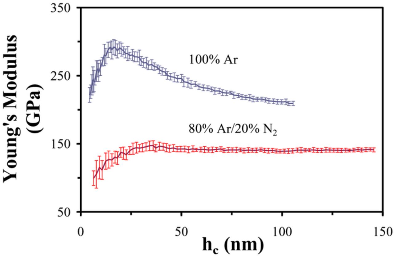
Figure 3. Nanoindentation Young's modulus as a function of indentation depth (hc) for two BCN films sputter deposited using C and BN targets with and without N2 working gas.
Figures 4 and 5 present nanoindentation Young's modulus (E) and hardness (H) results as a function of N2/Ar gas ratio for the BCN films sputter deposited using the C/BN and B4C/BN targets, respectively. For films deposited using pure Ar and either set of targets, high values of Young's modulus (∼ 285 GPa) and hardness (30–40 GPa) were observed. These values are consistent with the relatively high values of Young's modulus that have been previously reported for B4C and sputter deposited amorphous carbon films.11,50 However as both Figure 3 and 4 illustrate, these large values decreased significantly with the addition of N2 and remained essentially invariant at 100–150 GPa and 6–13 GPa with further addition up to 100% N2. This is consistent with the significant decrease in mass density that was also observed when N2 was added to the Ar sputtering gas.
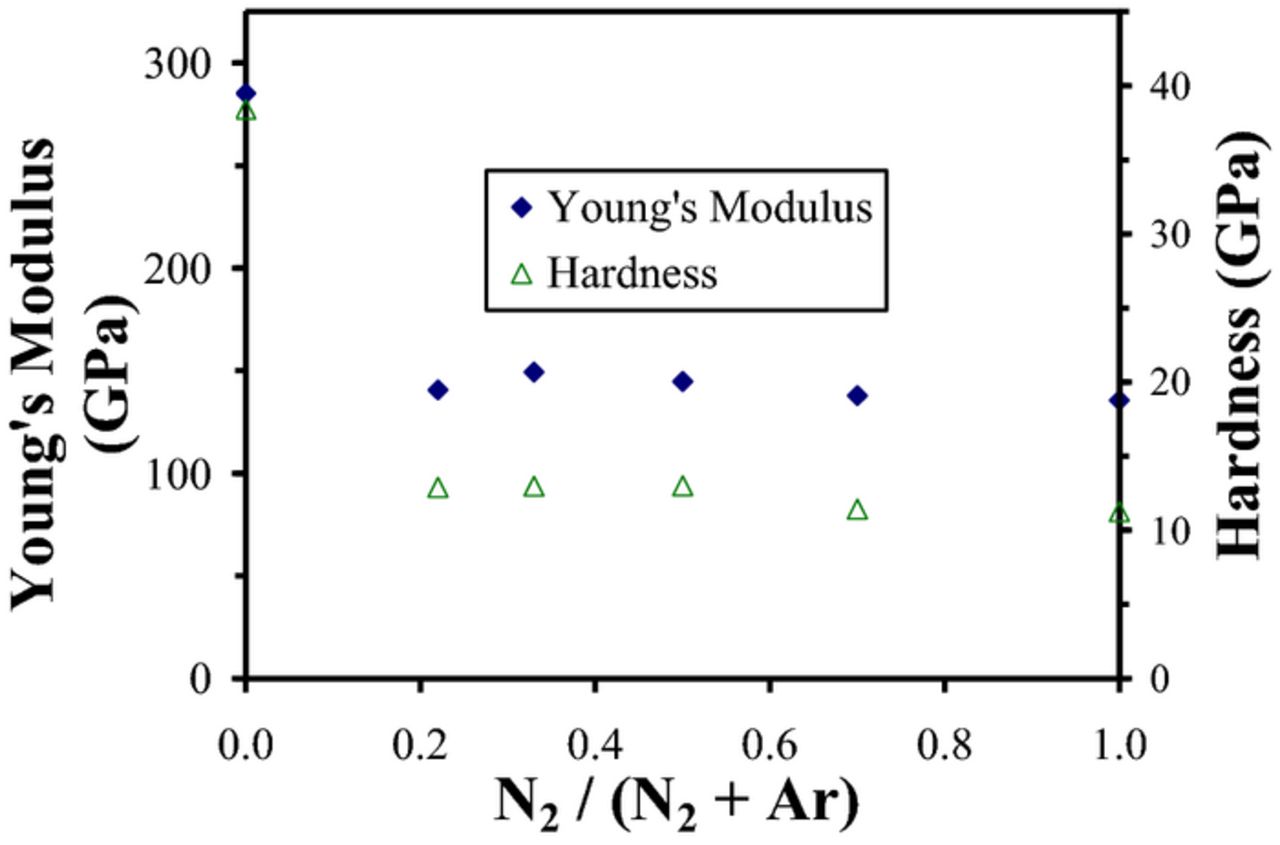
Figure 4. Nanoindentation Young's modulus and hardness as a function of N2/(N2+Ar) gas ratio for BCN films sputter deposited using C and BN targets.
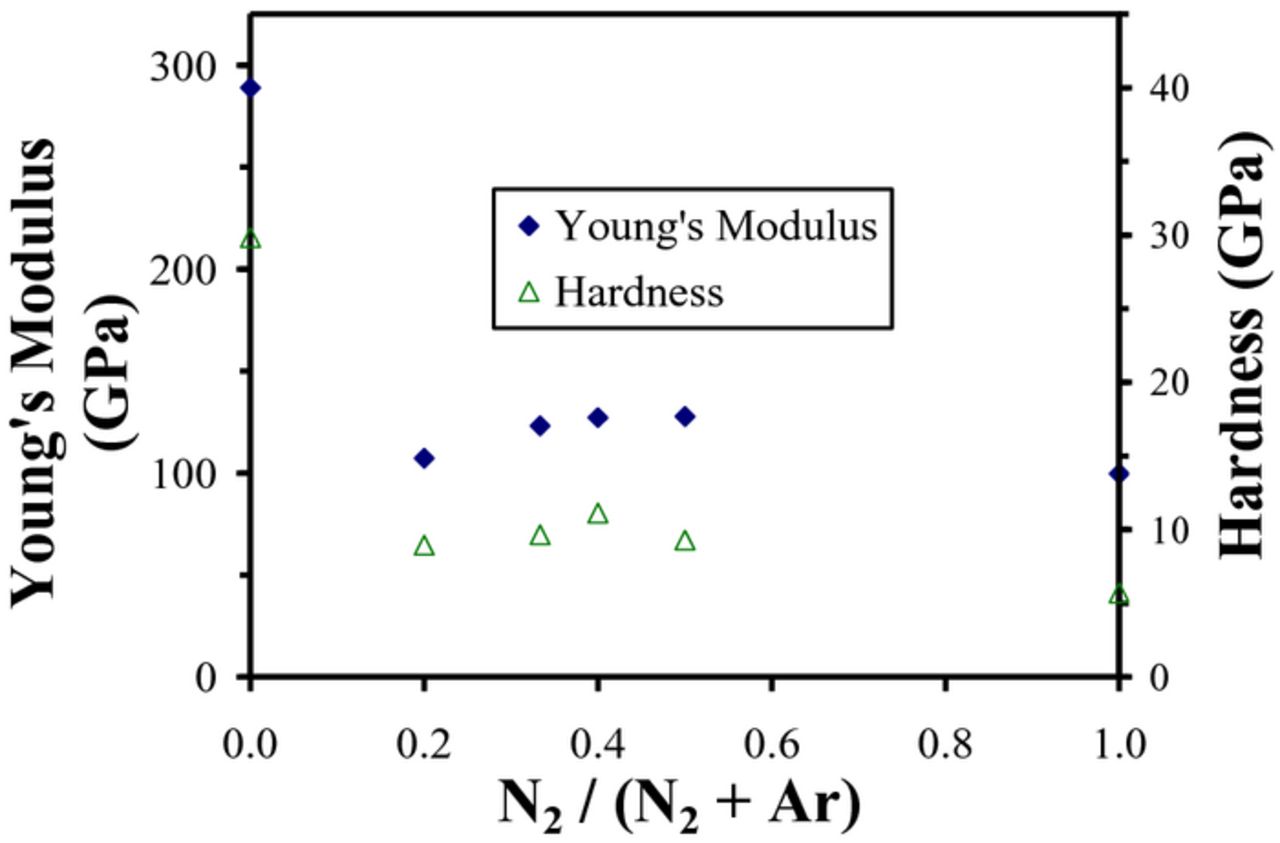
Figure 5. Nanoindentation Young's modulus and hardness as a function of N2/(N2+Ar) gas ratio for BCN films sputter deposited using B4C and BN targets.
The decrease in BCN mechanical properties with addition of N2 sputtering gas is also consistent with the change in composition of the deposited films where the films sputtered in pure Ar were boron or carbon rich while those sputtered in Ar/N2 mixtures were closer to BN in composition and sp2/h-BN in chemical structure. Reduced mechanical properties for BCN films have been previously reported. For example, Perrone et al. have reported microhardness values of ∼ 2.9GPa for BCN films deposited using pulsed laser ablation of graphite and hexagonal boron nitride (h-BN) targets.28 Tsai et.al. have also reported similar microhardness values of 1–3 GPa for cathodic arc plasma deposited BCN films.51 Thus, the observed mechanical properties for the BCN films deposited here are consistent with the literature and the reduced mechanical properties for the Ar/N2 sputter deposited films can be attributed to the predominate BN composition and sp2/h-BCN chemical structure.
Included in Table III are the nanoindentation Young's modulus and hardness values for BCN films sputter deposited using B4C and BN targets with various DC and RF biases. High modulus and hardness values exceeding 250 and 25 GPa, respectively, were observed in all cases. This is consistent with the high B content and BC structure exhibited by these films. Unfortunately, no clear trends were observable between the mechanical properties and the variation in DC and RF bias for the sample set investigated here. There are also no obvious correlations between the mechanical properties and the percentage or ratio of elements detected by XPS in these films.
However, the mechanical properties for this last set of BCN films were all high with a maximum nitrogen content of only 18%. In comparison, the minimum nitrogen content for the previous BCN sample sets was 24% and the mechanical properties were greatly reduced. This observation is consistent with a prior study of BCN by Martinez et.al where the hardest films were those with the lowest nitrogen concentration and a minimum in hardness was observed at a nitrogen concentration of ∼ 20%.13 Based on these observations, one may conclude that maintaining nitrogen content to < ∼ 20% may be ideal for achieving BCN films with the highest possible mechanical properties.
Conclusions
BCN thin films were deposited successfully by dual magnetron DC and RF sputtering from B4C/BN and C/BN targets in an N2/Ar ambient. Variations in BCN chemical composition and chemical bonding produced by sputtering with different N2/Ar ratios and DC/RF bias were investigated using XPS and FTIR and correlated to other physical, dielectric and mechanical properties such as mass density, dielectric constant, Young's modulus and hardness. Depending on the specific targets utilized, sputtering in pure Ar was observed to produce either carbon rich (C/BN targets) or boron rich (B4C/BN targets) BCN films with mass densities of 2.4–2.5 g/cm3 that approached the theoretical mass density for B4C (2.5 g/cm3). In nano-indentation measurements, these same films exhibited high values of Young's modulus and hardness of ∼285 GPa and 30–40 GPa, respectively. The addition of N2 to the Ar working gas lead to the incorporation of significantly more N (20–45%) and the formation of predominantly sp2/h-BCN structured films. The higher nitrogen content films exhibited reduced mass densities (2.0–2.1 g/cm3), low dielectric constants (3.9–4.6) and reduced values of Young's modulus (100–150 GPa) and hardness (6–13 GPa). Based on additional experiments varying the DC and RF biases, it was concluded that ∼ 20% nitrogen is a possible threshold for achieving BCN films with either high mechanical properties or electrically insulating properties with a low dielectric constant.