Abstract
The properties of thick GaN layers grown by metal organic chemical vapor deposition on 2'' HVPE substrates were investigated. Although the epilayer is smooth on a microscopic scale with high quality layers as evidenced by X-ray diffraction and photoluminescence, macroscopic morphological variations are observed on the wafer surface. These variations correspond to disparities in leakage current in fabricated Schottky barrier diodes, with rougher macroscopic morphology resulting in increased leakage current.
Export citation and abstract BibTeX RIS

This is an open access article distributed under the terms of the Creative Commons Attribution Non-Commercial No Derivatives 4.0 License (CC BY-NC-ND, http://creativecommons.org/licenses/by-nc-nd/4.0/), which permits non-commercial reuse, distribution, and reproduction in any medium, provided the original work is not changed in any way and is properly cited. For permission for commercial reuse, please email: oa@electrochem.org.
GaN-based technology has found widespread success in the electronic and optoelectronic fields, both as transistors and LEDs.1–3 These successes are mainly based on lateral device geometries or thin vertical structures based on heteroepitaxy on non-native substrates. While monolithic microwave integrated circuits (MMICs) based on high electron mobility transistor (HEMT) structures have enjoyed great success as RF power amplifiers, the lateral device geometry presents fundamental limitations, particularly for breakdown voltage, thus limiting applications for high power switching.4–8 To overcome some of these limitations and reach the full potential of the material for power devices, the next-generation of GaN power switching devices needs to move to a vertical geometry, which is enabled by the commercial availability of high quality, freestanding GaN substrates produced by hydride vapor phase epitaxy (HVPE) or ammonothermal growth.9 Homoepitaxial growth of power device quality GaN films on native substrates presents unique challenges from preparing the surface for growth, both to remove impurities and reduce thermal decomposition, to reducing impurities in the film for thick drift layers.10–13 This work will evaluate GaN films grown by MOCVD on HVPE substrates to understand the impact of surface roughness on Shcottky barrier diode performance to evaluate metrics for evaluating epitaxial layer quality and uniformity.
The samples in this study were grown in an Emcore D-180 metal organic chemical vapor deposition (MOCVD) reactor on a commercially-sourced, 2'' freestanding n+ GaN substrate from Kyma Technologies grown by HVPE. The MOCVD growth consisted of 5 μm of unintentionally doped GaN using standard growth conditions (3000 V/III, 200 Torr, 1030°C) and precursors (trimethylgallium and ammonia). Secondary ion mass spectroscopy (SIMS) measurements on films from this reactor under these growth conditions indicate background oxygen and carbon impurities at detection limits and a Si concentration of ∼2 × 1016 cm−3. As the substrate was received polished to an epi-ready surface, no additional in-situ or ex-situ cleaning procedures were undertaken. After growth, the surface morphology was characterized using multiple techniques to evaluate many length scales, including optical microscopy, atomic force microscopy (AFM), and optical profilometry. In addition, photoluminescence (PL), X-ray diffraction (XRD), and wafer bow were investigated to assess material quality.
XRD maps were taken of the wafer using a PANalytical X'Pert MRD system (Cu Kα1 line) system, with a resolution limit of ∼12 arcsec. The full width at half maximum (FWHM) of the (0002) peak ranged from 71–176 arcsec, consistent with freestanding GaN films. Maps of the FWHM of the (002) and (105) reflections are shown in Figure 1. The large variation across the sample indicates substantial lattice bow, which was confirmed with measurements before and after growth. The maximum bow was ∼20 μm and did not change significantly after epitaxial growth. The photoluminescence spectrum was taken both before and after epitaxial growth at room temperature and 77 K using a 325 nm He-Cd laser and is shown in Figure 2. Of particular interest is the broad defect band luminescence in the visible region. The as-received substrate exhibits luminescence in the orange band, which in HVPE substrates has been attributed to transitions from shallow donors to a deep-level defect.14 However, the epitaxial layer exhibits typical yellow band luminescence consistent with MOCVD GaN, indicating that the impurities from the HVPE substrate do not propagate through the active device layers. By taking the PL spectrum at 77 K, the thermal broadening is removed near the band edge, revealing four peaks which are associated with free exciton excitations, stacking faults, or dislocations.15,16 AFM images were taken with a Bruker Dimension FastScan. Representative images (Figure 3) show smooth samples, with steps clearly visible at both 10 × 10 μm and 1 × 1 μm scan sizes. Respective rms roughness values were 0.49 nm and 0.07 nm for the two scans. On this scale, no real variation was seen across the sample surface after leveling to take into account larger scale morphology. However, at larger scales on the order of 100–1000 μm that are accessible through optical microscopy and profilometry, variations in wafer morphology were observed. These differences across a single wafer are illustrated in optical profilometry images taken at 250 × 250 μm scan sizes (Figure 4). Hillock morphology with an rms roughness of 60 nm is shown in Figure 4a, while Figure 4b shows much smoother morphology with an rms roughness of 14 nm. This hillock morphology has been seen previously, and is thought to arise from threading screw dislocations.17
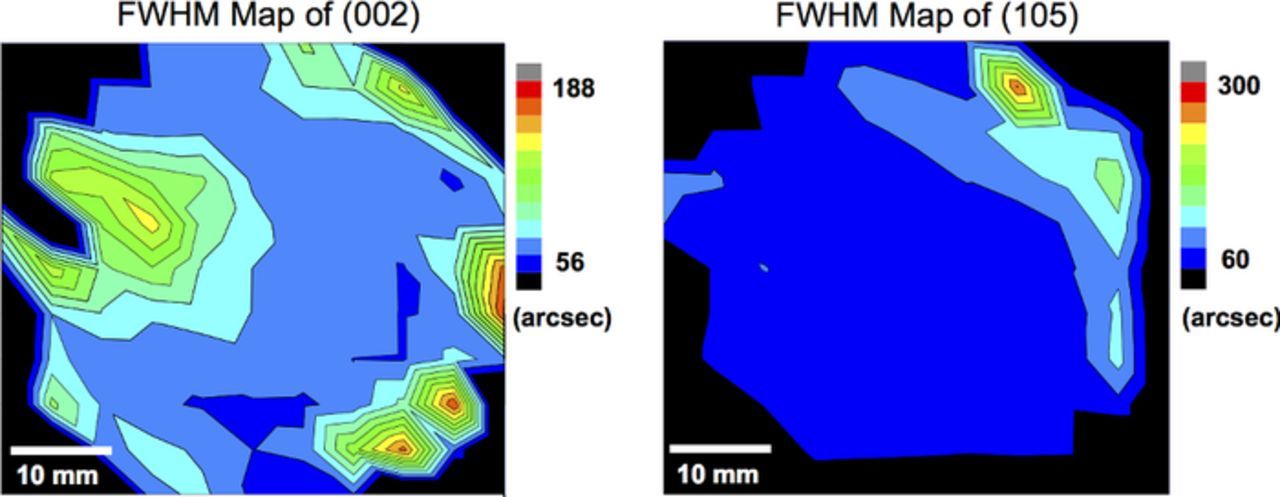
Figure 1. XRD FWHM maps of the (002) and (105) reflections.
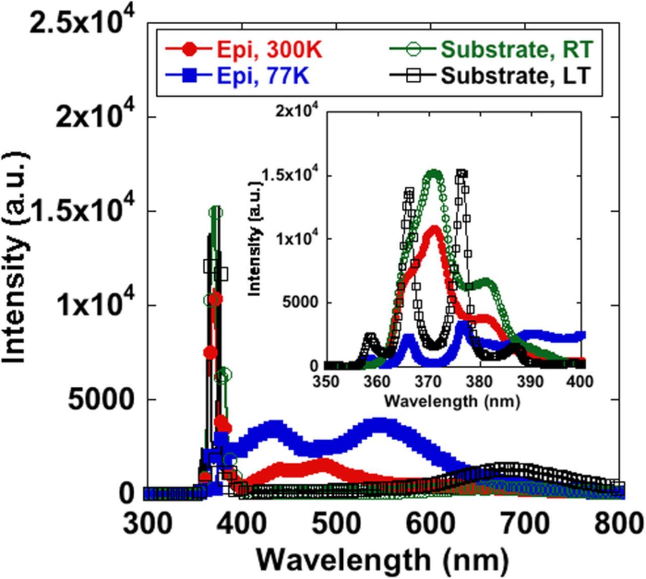
Figure 2. Photoluminescence spectra for substrate and epitaxial layers at room temperature and 77 K.
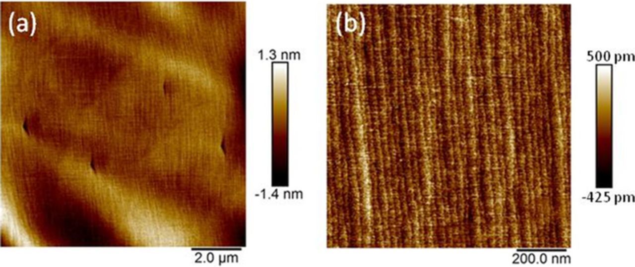
Figure 3. Representative AFM images with scan sizes (a) 10 × 10 um and (b) 1 × 1 um showing smooth, stepped growth.
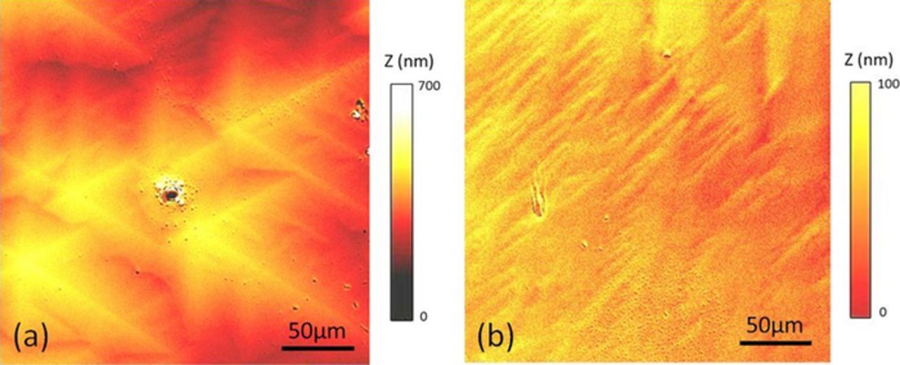
Figure 4. Optical profilometry images showing (a) rough, hillock morphology and (b) smooth surface morphology.
To understand how these materials properties affect electrical performance, vertical Schottky barrier diode (SBD) structures were fabricated on coupons of material exhibiting a representative range of roughnesses. Simple circular diode structures from 50–500 μm in diameter were formed by lift-off of E-beam deposited Ni/Au (20/200 nm) on the top side and blanket Ti/Al/Ni/Au (20/120/40/80 nm) on the back side. The diode forward and reverse characteristics are shown in Figure 5. It is clear that there is a variation in leakage current of over 5 orders of magnitude among the different regions measured. Furthermore, analysis of barrier height (ΦB) and ideality factor (η) from the Richardson equation, summarized in Table I, indicate a decreased barrier height and increased ideality factor in the regions of high leakage current. The regions of high leakage correspond directly to the regions of high surface roughness observed in optical profilometry. We propose that the mechanism for this effect is related to variation on offcut angle across the wafer, leading to a variation in localized growth kinetics and thus impurity activation. In addition, the typical clusters of defects such as dislocations and V-pits are sporadically observed and may be impacting performance. Breakdown voltage, shown in Figure 6 and summarized in Table I, follows a similar trend. The breakdown voltage is likely degraded in regions of high surface morphology due to both the increased leakage current as well as field concentration at the top of the hillocks. However, in the regions where smooth films were achieved over large length scales, the reported breakdown voltage of 700 V in a 5 μm film represents a critical field of 1.4 MV/cm, an exceptional result for a simple structure with no field management.
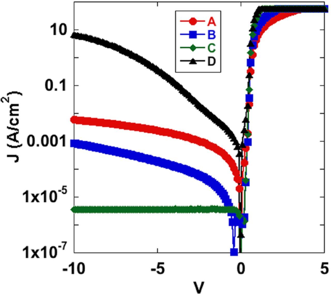
Figure 5. Diode I-V sweep.
Table I. Summary of Relevant Device Parameters.
| Device | A | B | C | D |
|---|---|---|---|---|
| RMS (nm) 250 × 250 μm | 59.65 | 22.36 | 14.40 | 94.17 |
| ΦB (eV) | 0.932 | 1.15 | 1.14 | 0.803 |
| η | 2.16 | 1.07 | 1.06 | 3.85 |
| VBR (V) | −590 | −620 | −670 | −30 |
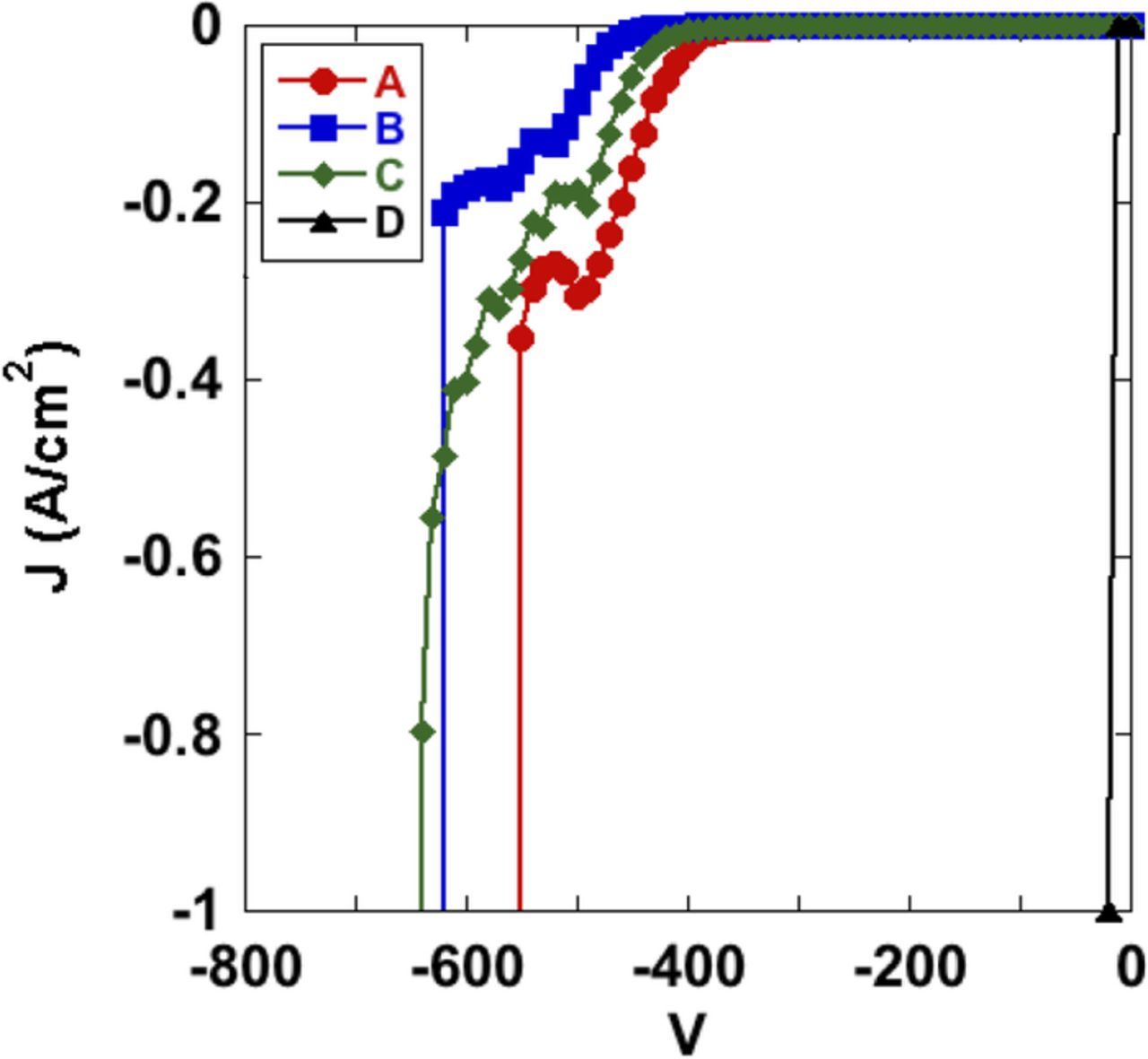
Figure 6. Breakdown voltage measurement at sweep rate of 10 V/s.
In conclusion, the growth and preliminary characterization of high performance MOCVD epitaxial layers on HVPE substrates has been demonstrated. The results show that surface roughness can be employed as a metric to screen epitaxial layers, where substantial variation on offcut angle across the substrate acts as a potential limitation to epitaxial layer uniformity and repeatability. However, in the best regions of the wafer, high critical fields are supported, indicating that with appropriate field mitigation this material is suitable for kV-class power devices.
Acknowledgments
This research was performed while L. E. Luna held a National Research Council Research Associateship Award at the U. S. Naval Research Laboratory. J. C. Gallagher gratefully acknowledges the support of the American Association for Engineering Education NRL Postdoctoral Fellow Program. Research at NRL is supported by the Office of Naval Research. The authors acknowledge the NRL Institute for Nanoscience (A. Boyd, D. St. Amand, and W. Spratt) for fabrication support.