
Abstract
To support the feasibility of an all-Si tandem solar cell based on quantum confined Si nanowires, we investigate the diameter reduction of nanowires by thermal oxidation. As a starting point, 6 × 6 mm2 arrays of vertical nanowires with a 90-nm pitch were made by DUV lithography and anisotropic reactive ion etching. These arrays are subsequently oxidized at temperatures ranging from 825°C to 1150°C. The lower temperature oxidation results in retarded oxidation kinetics, as expected. An unexpected gradual necking and undercutting of the nanowires is however observed for all oxidation temperatures. The effect of temperature on the stress buildup is investigated by process simulation and an eventual solution to the necking problem is found in a two-step oxidation process. This process consists of stopping the oxidation before any necking occurs and removing the oxide before further oxidizing the nanowires to obtain the desired core diameter.
Export citation and abstract BibTeX RIS
In the field of photovoltaics the goal of ongoing research is the reduction of the cost per Watt peak. This battle can be fought on two fronts: either a reduction in cost (for instance by a reduction in highly purified silicon through the use of thinner wafers) or an increase in efficiency. This increase in efficiency has a theoretical maximum generally known as the Shockley-Queisser limit. For a crystalline Si device with a single p-n junction under AM1.5 illumination this theoretical efficiency limit is about 30%.1 When a crystalline Si (Eg = 1.12 eV) bottom cell is combined with a top cell with a bandgap around 1.7–1.8 eV in a tandem cell structure, this efficiency limit can be increased to about 40%.1 To make this device entirely in Si would avoid the use of costly materials such as III-V semiconductors. Current all-Si tandem cells are either based on a-Si or Si quantum dots as high-bandgap Si material. The Si quantum dot approach was initially proposed by Green et al.2 Si quantum dots were embedded in a dielectric matrix and were shown to have an increased bandgap varying with the size of the quantum dots. This approach has been popular thanks to the relative simplicity of the fabrication of quantum dots. Both materials, however, have drawbacks for obtaining high currents. In the a-Si (micromorph) approach, the short-circuit current of the cell is limited by the poor quality of the material of the top-cell. The drawback of the quantum dot approach is the need to tunnel through the dielectric matrix in-between dots to drive the current to the electrodes and the resulting sensitivity of the device to dot and barrier size and size distribution. Therefore we propose an alternative embodiment (see Figure 1) making use of quantum wires. Our approach is to engineer the bandgap of Si by 2D-quantum confinement in very thin Si nanowires to create a higher bandgap c-Si material. The last dimension is not confined to allow the current to flow. For a proof of concept the initial synthesis relies on lithography and dry etching, although this will obviously have to be replaced by cost-effective synthesis methods for industrial application down the line (i.e. VLS growth, Ag based etching, etc.).
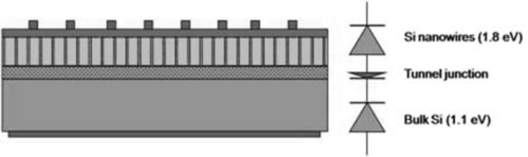
Figure 1. Graphical representation of an all-Si-based tandem solar cell with a Si-nanowire top cell.
Thermal oxidation of cylindrical structures has been investigated in the past3–5 and the oxide growth rate was reported to differ from what is described in the Deal-Groove model for flat surfaces. These differences were shown to be even more pronounced for structures with very high curvature and it was shown that there was a self-limiting effect in the oxidation of nanowires at temperatures below the point of viscous flow of oxide.6–8 These investigations suggest that the slower oxidation of the Si is due to the development of stress during the oxidation process. On the other hand, at higher temperatures the viscous flow of the oxides releases the stress in the oxide, allowing corner rounding.9 An added benefit of thermal oxide grown at higher temperatures is the improved Si/SiO2 interface quality.10 The purpose of our work is to investigate whether thermal oxidation can be used to yield densely packed arrays of 500-nm-long Si nanowires with diameters below 5 nm.
Experimental
The effect of quantum confinement in Si nanowires only manifests itself for diameters below 5 nm. It is very challenging to make Si nanowires of this size in one step by lithography and dry etching. Hence the target dimension after lithography is set around 45 nm and further size reduction is done by thermal oxidation. The material used is 100-oriented 1 Ω ⋅ cm p-type CZ Si wafers of 300 mm diameter. First the patterning stack is deposited on the wafer. This stack consists of a 250 nm hardmask (Advanced Patterning Film which is an amorphous carbon layer), 35 nm dielectric anti-reflective coating (SiOC), 38 nm bottom anti-reflective coating (ARC29sr-303) and 105 nm photoresist (AIM5484). The pillars are defined by double-patterning a mask consisting of 45 nm lines with a 90 nm pitch by deep UV lithography (see Figure 2). The mask is rotated ∼91° between the two expositions in order to obtain a tilted array of dots in the resist.
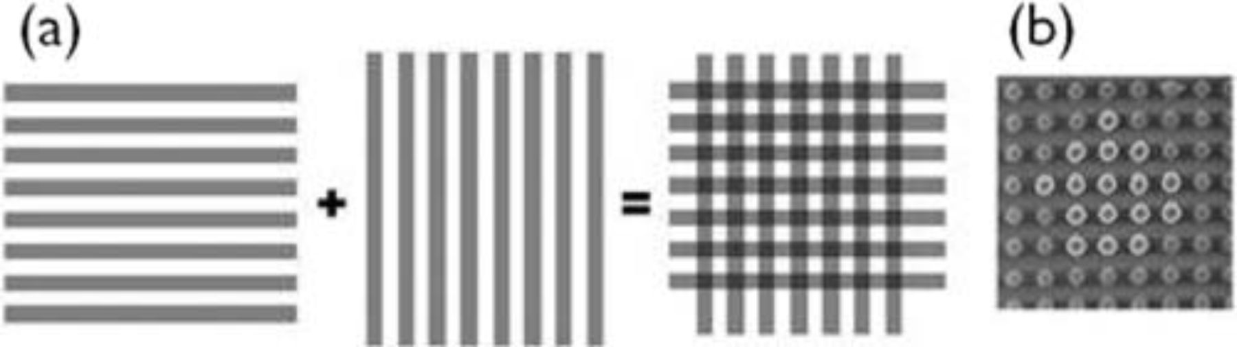
Figure 2. (a) Diagram of the mask and the double-patterning DUV lithography process, (b) top-view SEM of pattern in resist.
Subsequent dry etching is performed on the 2300 Kiyo C Series conductor etch system from Lam Research, with different etch chemistries to transfer the pattern through each of the layers of the patterning stack. The final Si etch is performed with a mixture of SF6, CH2F2 and N2/He. After the Si etch a dry in-situ strip is performed to remove residual APF. The particular etch recipe used in this instance wasn't optimized for within wafer uniformity. Figure 3 compares the resulting nanowires in the center die (# 0) and in a die on the edge of the wafer (# 10). There is a significant die-to-die non-uniformity in terms of etch-depth, nanowire diameter and tapering of the nanowires. This is plotted in Figure 4 where diameters from 3 locations along the length of the nanowires measured by cross-section SEM are compared with a top-view measurement of the diameter (CDSEM). After dry etch the bottom of the nanowires ranges from 55 to 25 nm from the center to the edge of the wafer, while the middle of the nanowires ranges from 35 to 24 nm. Etch recipes with significantly better within wafer uniformity were also developed but since the eventual goal is to investigate quantum size effects in function of the diameter, the non-uniform recipe was used to our advantage for this work. This reduced tapering combined with the slightly increased height of the nanowires, make the dies on the outside of the wafer more interesting for application in this type of photovoltaic device.
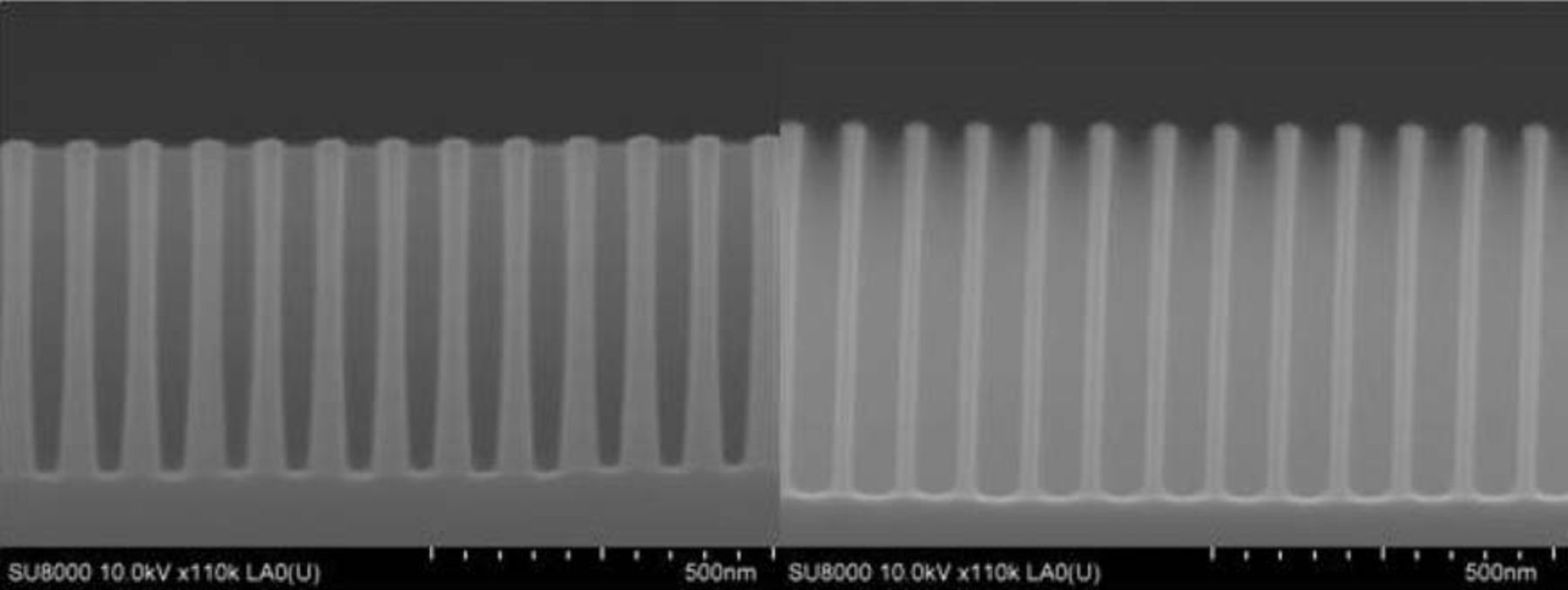
Figure 3. SEM images comparing the center die (left) with a die on the edge of the wafer (right) after dry etching, before oxidation.
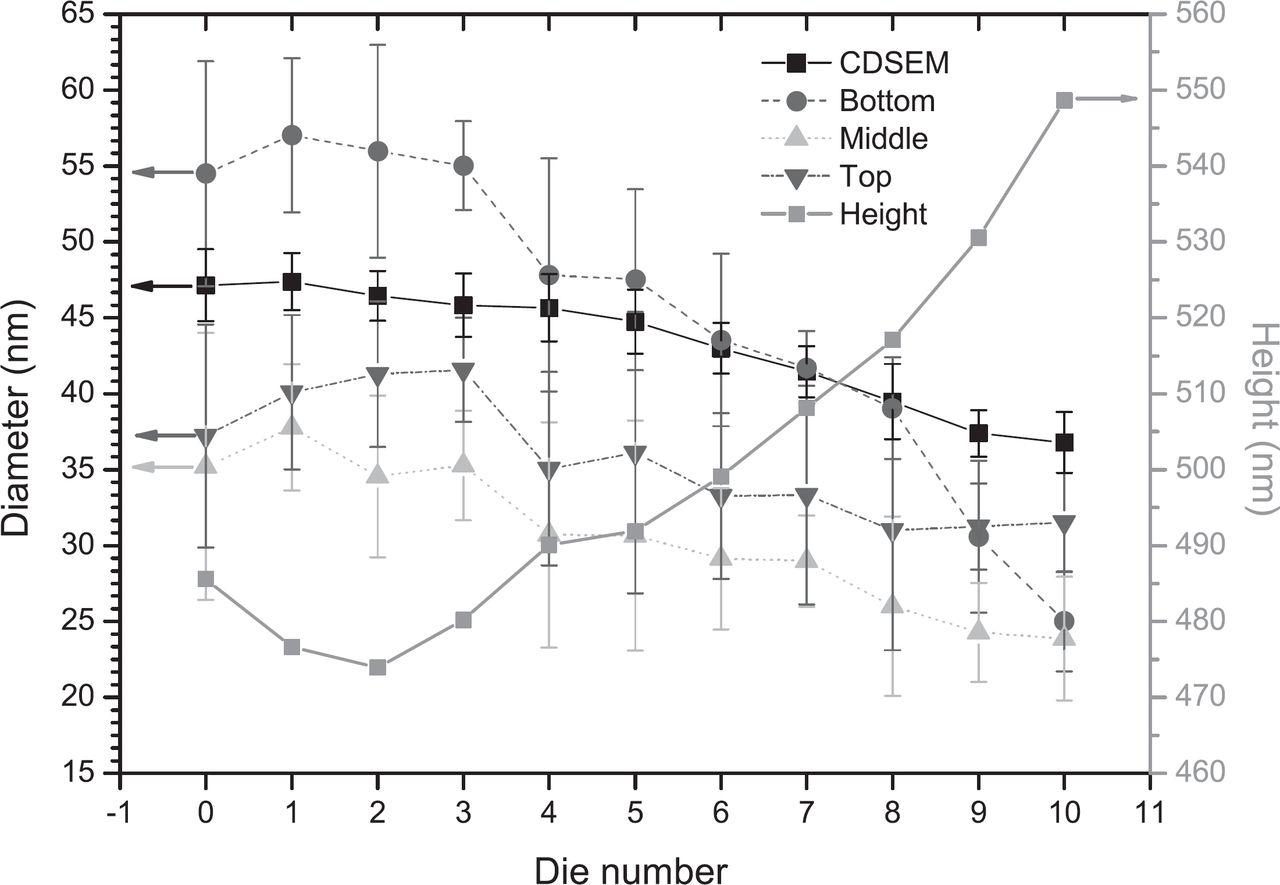
Figure 4. Plot of the diameter measured by top-view SEM (CDSEM) and measured by cross-section SEM at 3 locations along the length of the nanowires in function of the die number. In addition the height is plotted in function of the die number.
Multiple oxidation conditions were used to reduce the as-etched diameter of the Si nanowires. The samples were oxidized for different durations in pure oxygen in a furnace at 825°C, 925°C and 1025°C. Further experiments were also performed in a rapid thermal oxidation furnace at 1150°C both in pure oxygen and a mixture of oxygen and nitrogen.
For characterization and imaging a dual beam FIB/SEM Nova600i and Strata400 (both FEI) were used for sample preparation. A Tecnai F30 ST from FEI was used for the microscopy. A cap layer is needed to protect the surface during FIB specimen preparation and therefore a sputtered SiO2 layer is used. As visible on TEM images due to its darker contrast compared to thermally grown oxide, the sputtered glass does not fill the high aspect ratio structure (see for instance Figure 5). Partial overlap of 2 rows of nanowires can occur since the pitch is only 90 nm and the sample thickness is ∼100 nm. Dimensional data were measured from TEM micrographs at fixed positions along the nanowire height referenced to the top edge.
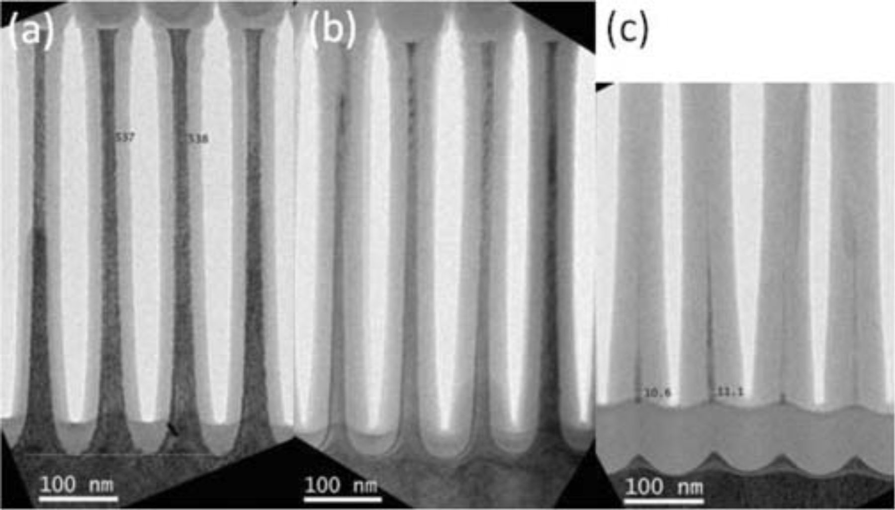
Figure 5. TEM picture for samples with the same starting diameter after 2 hours of oxidation for (a) 825°C, (b) 925°C and (c) 1025°C.
Results
Examples of the Si-SiO2 core-shell structures obtained for the same starting diameter after 2 h oxidation at 825°C, 925°C and 1025°C are shown in the TEM images of Figure 5. The darkest gray corresponds to crystalline Si, the medium gray to SiO2, whereas the lightest gray corresponds to the void between the NWs. The oxide grown in the concave parts between the nanowires sometimes also has a slightly different contrast from that around the nanowires. This is due to fact that this region (grown from the bulk) has the dimension of the slice; while the NW part is thinner.
The thicknesses of the Si core and the SiO2 shell depend on the oxidation temperature. For 1025°C it can be seen that most of the nanowire is oxidized and an oxide layer has formed between the substrate and the nanowires. For 825°C and 925°C there is still a Si core connected to the substrate after 2 hours. The temperature dependence of the thickness of the oxide grown in the concave part between the nanowires is more pronounced than that of the oxide around the nanowires.
For 925°C an overview of the evolution of the Si core and the SiO2 shell thicknesses as a function of oxidation time is given in Figure 6. The TEM-measured thickness of the oxide surrounding the nanowires at different locations along the nanowire is plotted together with the thickness of the oxide grown on a flat part of the same substrate to make the comparison with the oxidation rate of flat Si. The starting core diameters of the foot, middle and top of the NW are 64, 50 and 43 nm respectively. Additionally the thickness of the oxide in the concave part between the nanowires is also plotted.
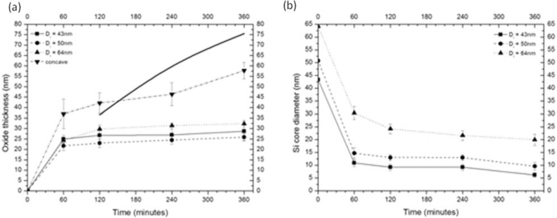
Figure 6. (a) Oxide thickness in function of time at 925°C: comparison between the oxide grown on blanket Si (thick black line), the nanowire oxide thickness and the oxide thickness in the concave part between nanowires, and (b) Si core diameters in function of oxidation time for different locations along the length of the nanowire. The starting diameters of 64 nm, 50 nm and 43 nm are for the foot, middle and top of the nanowire respectively.
It can be seen that there is very little further oxide growth on the nanowires after 2 hours. The thickness of the flat oxide however continues to increase. This difference is consistent with previous reports on self-limiting or retarded oxidation of Si nanowires.6–13 The core reduction rate becomes extremely slow after 2 hours but doesn't stop entirely.
The final Si core diameter depends on the location along the nanowire. In the narrowest part of the nanowires this results in 6 nm after 6 hours of oxidation. At the bottom of the nanowires this results in 20 nm after 6 hours of oxidation. At higher temperature (i.e. 1025°C), the oxidation process shows much less self-limiting behavior, and continues until almost no c-Si remains, see Figure 5c.
The rate of oxidation of Si nanowires clearly deviates from the rate of oxidation of a flat Si surface. The important factors underlying this retarded oxidation are the large curvature of the Si surface and the low temperatures used. The large curvature imposes compressive stress of the oxide in the radial direction due to volume expansion in the incorporation of O-atoms while forming SiO2. When oxidation takes place at low temperature, the viscosity is very high and the stress builds up in the oxide. The consequence is reduced oxygen diffusion as well as reduced chemical reaction kinetics at the interface both leading to reduced oxidation rates.14 There is still a discussion in literature which of the two effects is dominating.15
In Figure 7 the behavior at the foot of the nanowires is compared for 2, 4 and 6 hours of oxidation at 925°C. The bottom of the nanowires starts necking after 4 hours and the nanowires are completely disconnected from the substrate after 6 hours. At that point the oxide starts growing under the nanowires, in similar fashion to what happens at 1025°C (see Figure 5c). Closer inspection of these TEM measurements showed some stacking faults and contrast related to strain. Metal contaminants are also being gettered to the foot of the nanowires and are sometimes found decorating the stacking faults.
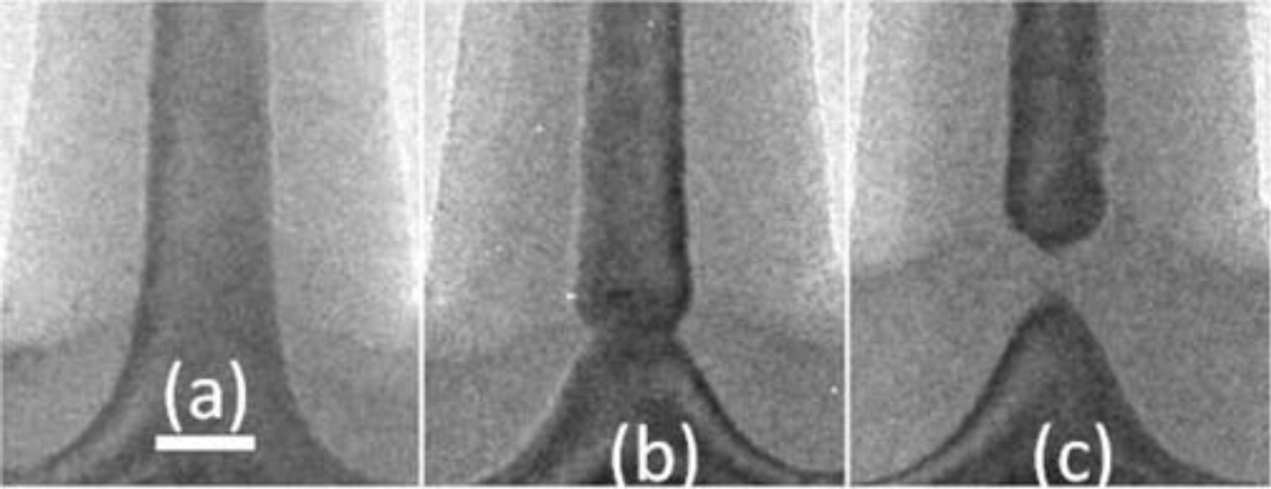
Figure 7. Comparison of the behavior at the bottom of the nanowire for oxidation at 925°C for 2, 4 and 6 hours (resp. (a), (b), (c)). The scale bar is 20 nm.
The effect of necking is also linked to the starting diameter, where bigger diameter nanowires show less necking than smaller diameter nanowires. This behavior was for example found for oxidation at 825°C, as can be seen in Figure 8 where nanowires from different dies were all oxidized for 6 hours. The inner die (8 (a)) has more pronounced tapering, displaying a thicker foot and no visible necking. The outer dies (8 (b,c,d)) have less tapering, a smaller initial foot and show increased necking and eventual undercutting with decreasing size of the initial foot. The thickness of the oxide in the concave part of the nanowires also gradually increases as the necking and undercutting progresses. So even though 6h oxidation at 825°C doesn't result in necking for thicker nanowires, it doesn't result in the small diameters of interest. Reducing the starting diameter however quickly leads back to necking. Experimental description and study of this necking and undercutting of the nanowires has not previously been reported in literature to the best of our knowledge.
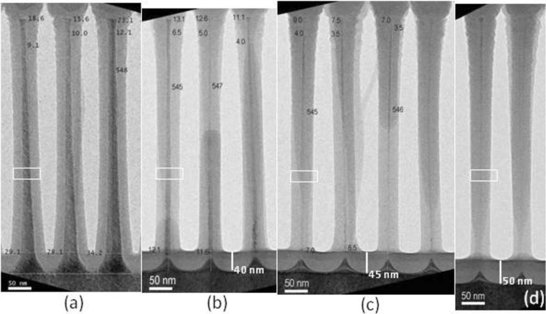
Figure 8. Comparison of the behavior at the bottom of the nanowire for oxidation at 825°C for 6 hours for different dies with decreasing initial size of the nanowires. The images are aligned to the top of the Si cores. The white rectangle indicates the size of the Si core plus oxide shell of the nanowires in (a) to visualize the decrease in diameter for (b–d). The inner die (a) shows more tapering and has a broader foot without visible necking. The smaller the initial diameter of the foot, the more pronounced the necking or undercutting.
Discussion
Liu et al.7,8, describes that the time needed to reach an asymptotic value for the Si core through self-limiting oxidation depends on the temperature: 5 hours at 850°C and 2 hours at 950°C. Therefore the oxidation time in our experiments extends to 6 hours for both temperatures to guarantee that the asymptotic value is reached. In contrast to their results, the nanowires started necking after 4 hours and were completely disconnected from the substrate after 6 hours (see Figure 7). In order to make a device it is paramount to avoid the necking and undercutting. However, this phenomenon has not been reported in literature; hence the interpretation of the observation is not straightforward. The effect bares some similarities with undercutting oxidation of scalloped sidewalls of tall Si ridges.16
Intuitively it seems that the nanowires are breaking due to the buildup of stress from the growing oxide. As a result one would think that higher temperatures would allow viscous flow of the oxide and relaxation of this stress. As already shown however, oxidation at 1025°C also results in undercut nanowires. The same occured for a 120 s rapid thermal oxidation at 1150°C in pure oxygen, indicating that viscous flow of the oxide doesn't alleviate the problem. Even for oxidation using in-situ steam generation at 1100°C similar necking behavior was seen, regardless of the improved viscous flow and the different kinetics17 accompanying oxidation by in-situ steam generation.
A molecular dynamics study of the strain distribution in oxidized nanowires by Ohta et al.16 can provide a starting point to gain understanding of this phenomenon. They have modeled a wire-shaped nanostructure of 3–5 nm high, and then an oxide film with a uniform thickness was formed by inserting oxygen atom into Si-Si bonds from the surface. The simulated structures show a necking behavior at the foot which is very similar to our experimental results. The stress in their Si structures is tensile perpendicular to the substrate, seemingly pulling the nanowires off the substrate. In the direction parallel to the substrate, the Si lattice is under a strong compressive stress due to the sandwich structure between two oxide layers forming the sidewalls. The stress in the oxide is compressive in both directions and is highest in the corner between the wire and the substrate.
The previous remark seems to indicate that in the densely packed nanowire arrays under study in this report, the oxide growing at the foot of the nanowires cannot relax and places the nanowires under compressive stress parallel to the substrate. At the same time the oxide expansion along the direction perpendicular to the substrate is suppressed due to the top SiO2/Si interface. The oxide network is anchored by the Si lattice of the nanowire. In the sidewall oxide, the oxide network cannot expand in any direction. The expansion of the side oxide along the direction perpendicular to the substrate is suppressed by the sidewall SiO2/Si interface, and the expansion along the direction parallel to the substrate is suppressed by the structural anchoring at the substrate and the top oxide. An additional factor why these stresses can cause necking and disconnection in our case is the surface roughness and surface defects that may be present preferentially at the foot of the nanowire after dry etching and that may facilitate dislocation nucleation.
In order to assess the impact of temperature in relaxing the stresses by viscous flow, the oxidation process was modeled. This was done with the use of sprocess, the process simulation tool of Synopsis Sentaurus TCAD.19 The stress-dependent oxidation model, implemented in sprocess, is used. This model couples the oxidant diffusivity and reaction rate to the local stress field, as indicated by the following equations:
Surface reaction rate parameter
![Equation ([1])](https://content.cld.iop.org/journals/1945-7111/159/3/H300/revision1/jes_159_3_H300eqn1.jpg)
Oxidant diffusivity
![Equation ([2])](https://content.cld.iop.org/journals/1945-7111/159/3/H300/revision1/jes_159_3_H300eqn2.jpg)
in which σnn is the normal stress (positive sign for compression) acting on the Si/SiO2 interface, p is the hydrostatic pressure in the oxide and Vk, Vd are fitting parameters. The zero-stress parameters kso, Do are derived from the linear and parabolic rate constants for planar silicon oxidation. Dmax is the maximum value of D, which is also a fitting parameter. Additionally Sentaurus sprocess by default treats oxide as a viscoelastic material with a viscosity dependent on temperature and shear stress:
Oxide viscosity
![Equation ([3])](https://content.cld.iop.org/journals/1945-7111/159/3/H300/revision1/jes_159_3_H300eqn3.jpg)
with
![Equation ([4])](https://content.cld.iop.org/journals/1945-7111/159/3/H300/revision1/jes_159_3_H300eqn4.jpg)
in which σs is the shear-stress and Vo, viscosityo and viscosityW are fitting parameters. The zero-stress or linear viscosity, ηo, is a function of temperature. The stress-dependent oxidation is the same model as was initially used by Kao et al.21 and later on by Ma et al.20 and similar values for the fitting parameters have been taken. The parameters for the linear viscosity were taken from Hetherington et al.22 Table I contains an overview of the values of the fitting parameters.
Table I. Fitting parameters.
| Parameter | Value |
|---|---|
| Vk | 12.5 Å3 |
| Vd | 75 Å3 |
| Dmax/Do | 1.2 |
| Vo | 300 Å3 |
| Viscosityo | 1.9 10−8 poises |
| Viscosityw | 5.68 eV |
The structure is defined as being cylindrical with a symmetry element as in Figure 9: a nanowire of 500-nm height with a 15-nm radius and a broader foot of 25-nm radius. The substrate underneath has a width of 45 nm to represent the 90-nm pitch. The oxidation simulation was performed for 4 different temperatures (825°C, 925°C, 1125°C and 1150°C), each time with a different duration with as goal to reduce the core diameter to ∼4 nm for each temperature. In Figure 9 a zoom of the foot of the resulting structures for each temperature are plotted with the corresponding von Mises stress in Pa. A first comment to be made about these results is that the retarded oxidation rate of our Si nanowires is not quantitatively reproduced by this model. To model the retarded oxidation, the viscous flow model of Kao et al.3–5 was later on adapted by Liu et al. to explain their results of oxidation of nano-sized cylindrical structures.6–8 As more experimental results on nanowires became available, Cui et al. published a more detailed model with more accurate results.23 Additional papers by Ma and Fazzini provide further understanding of the physics.15,20, The implementation of these more complex models that more accurately predict the oxidation rate is outside the scope of this publication.
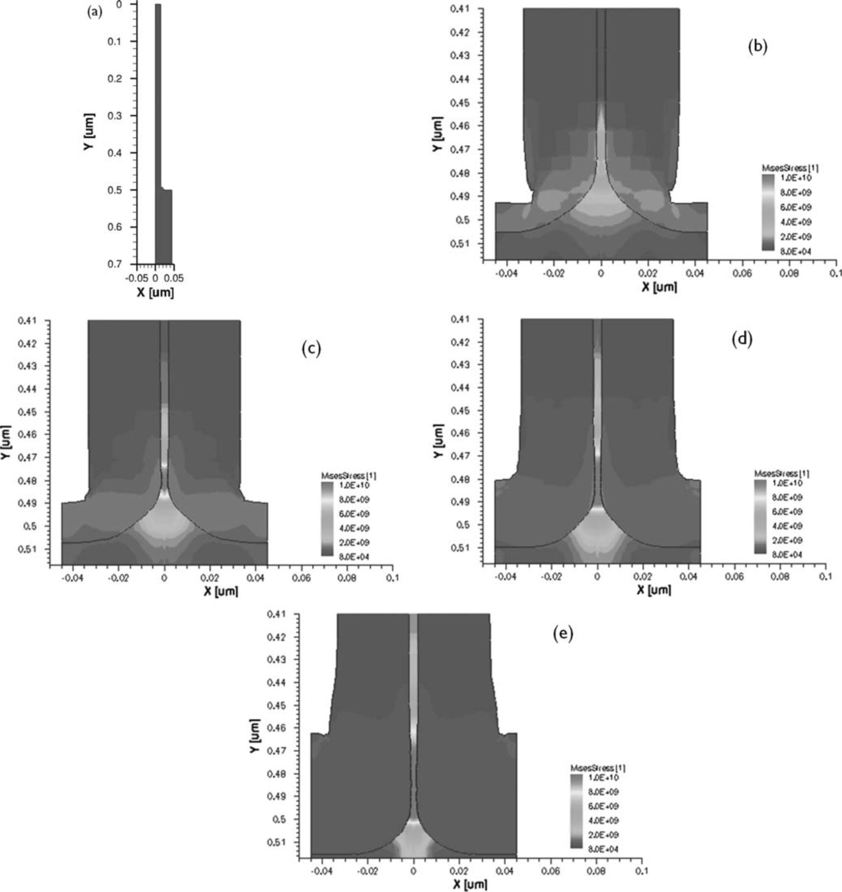
Figure 9. (a) symmetry element before oxidation, right hand side: Von Mises stress (in Pa) around the foot of the resulting structure after oxidation in pure oxygen to reach the same core diameter at different temperatures and times: (b) 825°C, 85 minutes (c) 925°C, 17 minutes (d) 1025°C, 4.3 minutes (e) 1150°C, 1 minute.
Nonetheless the results show that the stress is clearly the highest at the foot of the nanowire, in qualitative agreement to Ohta et al.18 The oxidation at 825°C shows the highest stress in the oxide, typically accompanied by the reduced oxide thickness according to the stress-dependent oxidation model. As the temperature increases the stress in the oxide is reduced and the oxide grown at the foot of the nanowire and the substrate part between the nanowires is thicker. The oxide thickness around the nanowires measured higher up is constant for all temperatures.
The stress in the Si follows the trend of the oxide thickness around the foot, increasing as the temperature goes up. The advancing oxide front creates a highly stressed Si neck which is slightly thinner than the rest of the nanowire higher up. At 1150°C the oxide around the foot has grown the most. This elongates the nanowire and creates a neck which is only ∼2 nm (instead of ∼4 nm higher up). This thinner neck region is also present for the other temperatures but less pronounced. The important outcome of the simulation is not the minor thinning but the localized stress buildup at the foot of the nanowires. It can be concluded that the necking doesn't have its origin from preferential oxidation at the foot.
The experimental necking and undercutting is much sharper than what is showing up in the simulations. The simulations however only look at the oxidation process, without looking at the fracture mechanics of the nanostructure. The mechanic properties of Si nanowires have been shown to differ from those of bulk Si.24,25, Han et al. report a brittle to ductile transition at room temperature for Si nanowires.26 In light of this, Kang et al. have performed molecular dynamics simulations on the effect of the diameter and the temperature on the fracture mechanisms of Si nanowires.27 They find that for temperatures above 1000 K nanowires with diameters larger than 4 nm will shear extensively prior to fracture. The experimentally observed necking does indeed occur for oxidation at temperatures of 825°C and higher. These particular fracture mechanisms are not included in the oxidation model but will clearly play a major role in understanding the necking. It can however be expected that the necking is a result of an interplay between oxidation and mechanical failure at the foot of the nanowires. The advancing oxide front creates a stressed neck, which is more likely to shear at the elevated temperature of oxidation. While shearing occurs, the oxidation continues.
Both experiments and simulation have shown that simply increasing the temperature to allow viscous flow of the oxide does not solve the necking problem. In order to further reduce the stress, a two step oxidation process is proposed. The two-step approach essentially consists of stopping the oxidation before signs of necking occur, removing the oxide and oxidizing the nanowires for a second time until the right size is obtained. The oxidation is done by rapid thermal oxidation at 1150°C, for 60 seconds and a flow of 5 slm O2 and 15 slm N2. Even though this temperature is out of the range where the self-limiting effect is expected, it was selected with the quality of the Si/SiO2 interface in mind. It is known that thermal oxides grown at higher temperatures offer the lowest amount of dangling bonds.10 Combined with the proper hydrogen anneal, this should give well-passivated interfaces. This is of course a very important aspect for device fabrication planned in the future. After oxide removal, the same oxidation step is repeated.
A dry oxide removal method is implemented to circumvent the drying problems occurring due to the capillary forces in these dense high-aspect ratio structures when working with wet HF cleans. In wet cleaning processes, capillary forces exerted on nano-structures during wafer drying can lead to bending and eventually stiction or collapse of neighboring features.28 The removal of the oxide is done in a Siconi preclean chamber, offered on the Applied Endura platform. It is a highly selective clean that chemically etches away oxide, preparing the surface for the next process step without leaving vacuum environment. The process selectively etches away oxide on wafers by a dry NF3/NH3 based chemical etch and an in-situ anneal is performed to remove any reaction residues.29
After the second oxidation step, the nanowires obtain the required diameters without any signs of necking at the foot, as seen in Figure 10. The foot of the nanowires ranges from 8 to 13 nm, while the top of the nanowires ranges from 2.5 to 4.5 nm. This fulfills the requirements relatively well, considering that the broader part at the foot tapers quite quickly into a much longer part with a constant small diameter. Further work will be dedicated to both optical and electrical characterization of the obtained structures with the idea of elucidating any quantum size effects.
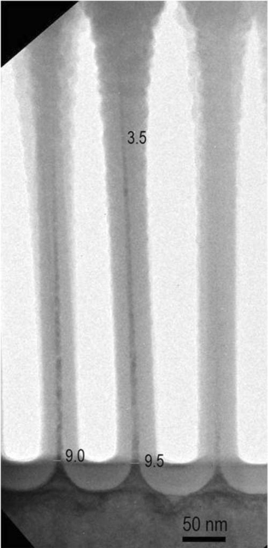
Figure 10. TEM picture after 2 steps of rapid thermal oxidation with intermediate dry oxide removal by siconi.
Conclusions
A dense array of vertical Si nanowires was made by 193 nm DUV immersion lithography and dry etching. The nanowires had a pitch of 90 nm, a height of 500 nm and a diameter varying from 55 to 25 nm depending on the location on the wafer (center to edge). Oxidation of these dense arrays at 825°C and 925°C exhibited a retarded oxidation rate compared to at surfaces. Furthermore oxidation at temperatures from 825°C to 1150°C resulted in necking at the foot of the nanowire, which eventually completely disconnects the Si core from the substrate. Process simulation of the oxidation shows that a lot of stress occurs at the foot of the nanowires due to the oxide growth. At higher temperatures the stress in the oxide is released by viscous flow but this only increases the stress in the Si cores. A two-step oxidation process was developed to reduce the stress at the foot of the nanowires. In this process the oxidation is stopped before any necking occurs and the grown oxide is removed before a second oxidation step reduces the Si core to the desired dimension. As a result, very small-diameter nanowires are obtained, tapering from 8–13 nm at the foot to 2.5–4.5 nm at the top. These nanowires seem to be ideal for investigation of quantum size effects and device fabrication.
Acknowledgments
The authors thank Katia Devriendt, Tom Vandeweyer and Christina Baerts for their help with the DUV lithography and dry etching, Jean-Luc Everaert for his help with the rapid thermal oxidation and Hugo Bender for the fruitful discussions and providing TEM characterization of the Si NWs. This work is made possible by the support of the Institute for the Promotion of Innovation by Science and Technology in Flanders, Belgium (IWT).