
Abstract
In this study we compare the growth of gallium oxide films by halide vapor phase epitaxy (HVPE) on various substrates under the same growth conditions. Gallium oxide films were deposited at 500 °C–600 °C on basal plane (0001) planar and patterned sapphire substrates, (0001) 2H-GaN, 4H-SiC, and  bulk β-Ga2O3 substrates. The layers were studied by X-ray diffraction (XRD), scanning electron microscopy (SEM), and cathodoluminescence (CL) techniques. Most of the films exhibit growth features of hexagonal symmetry. Sn-doped Ga2O3 films exhibit n-type electrical conductivity. Heterojunctions composed of n-type hexagonal Ga2O3:Sn and p-type GaN:Mg demonstrate diode-like I-V characteristics and emit light under forward bias.
Export citation and abstract BibTeX RIS

This is an open access article distributed under the terms of the Creative Commons Attribution 4.0 License (CC BY, http://creativecommons.org/licenses/by/4.0/), which permits unrestricted reuse of the work in any medium, provided the original work is properly cited.
In the last years, gallium oxide has attracted a lot of attention as a novel wide bandgap semiconductor material with high breakdown field.1,2 Gallium oxide exists in at least five polymorphic forms. The monoclinic β-form is the only polymorph stable through the whole temperature range up to the melting point. The researches were mainly focused on the β-Ga2O3 form as high quality large single crystals of this polymorph can be produced by melt growth methods such as Czochiralski, floating zone, and edge-defined film-fed growth. Recently, other metastable polymorphs, particularly the corundum-structured α and orthorhombic ε-Ga2O3 forms have attracted much attention.3–12 These polymorphs have highly symmetrical crystal structure and are epitaxially compatible with sapphire, III-nitrides, and silicon carbide.
First principle calculations predict that the ε-phase is the second most stable polymorph after β. XRD, TEM, and DSC measurements indicate that reconstruction of the crystal lattice of the ε-phase starts at temperatures above 650 °C. Rapid transition to β-phase occurs suddenly at 880 °C–920 °C.3 XRD studies showed that complete transformation from ε-Ga2O3 to β-Ga2O3 occurred only after annealing at 1000 °C.4
ε-Ga2O3 is the only Ga2O3 polymorph that exhibits ferroelectricity. The spontaneous polarization of ε-Ga2O3 is shown to be larger than that of GaN by theoretical studies and is predicted to achieve high two-dimensional electron gas (2DEG) density with high mobility. Owing to these properties, ε-Ga2O3 heterostructures are expected to form a 2DEG with high mobility and sheet carrier density.5 Due to the lack of inversion symmetry, ε-Ga2O3 has high dielectric constant κ of 32 at 10 kHz which is comparable to that of high-κ materials such as La2O3 and Hf2O3.5
The crystal structure of the ε-Ga2O3 polymorph remains controversial. Roy et al.6 who were the first to report this polymorph, failed to identify the crystalline structure of ε-Ga2O3 but concluded that its symmetry must be lower than hexagonal or tetragonal. More in-depth study by neutron diffraction by Playford et al.7 showed that it has a hexagonal structure similar to that of 2H-GaN with space group P63mc. However, these results possibly were affected by low phase purity of the studied material which was a mixture of ε-Ga2O3 (57%) and β-Ga2O3 (43%).
Recent experimental findings suggest that ε-Ga2O3 has orthorhombic crystal structure.5,8,9 M. Kracht et al. explained the hexagonal symmetry observed in ε-phase by twinning of three rotation domains of the orthorhombic κ-Ga2O3.9 TEM and XRD investigations of MOCVD layers revealed that the hexagonal P63mc structure consists indeed of orthorhombic Ga2O3 domains with Pna21 space group symmetry. The X-ray data of the orthorhombic Ga2O3 domains with {110} twin boundary [40] can be transformed to the hexagonal symmetry published by Playford et al.2
Similar results were obtained by Cora et al.10 who revealed the presence of orthorhombic κ-Ga2O3 rotation domains with Pna21 space group symmetry by high resolution TEM. The domains are very small so they can be detected only by electron diffraction at the nanoscale. When the domain size is smaller than the resolution of the probing technique, the hexagonal symmetry is recovered in the diffraction patterns.
One of the reasons for the formation of rotation domains in ε-Ga2O3 epitaxial films is the mismatch of rotational symmetry between the substrate and the epitaxial layer. Epitaxial growth of a crystalline material with a low degree of symmetry on a substrate with a high degree of symmetry results in rotational domains. Other mechanisms for the formation of rotational domains are also possible. Nishinaka et al.8 pointed out that the structure of the orthorhombic ε-Ga2O3 itself allows the occurrence of three rotational domains.
Crystalline films of ε-Ga2O3 can be produced by epitaxial growth techniques such as halide vapor phase epitaxy,11 metal organic chemical vapor deposition,10,12–15 mist chemical vapor deposition,8,16–21 and molecular beam epitaxy.9 The growth temperature is the crucial factor that controls the polymorphic composition of Ga2O3 layers. All reported films containing ε-Ga2O3 were grown at temperatures below 800 °C.4 However, low growth temperature is a necessary, but not a sufficient condition for the deposition of ε-Ga2O3. Although epitaxial growth at temperatures above 850 °C almost always results in the high temperature β-phase, deposition at lower temperatures can produce α, β, ε and other polymorphs. The phase composition of epitaxial films can be also controlled by gallium precursor, growth temperature, VI/III ratio, pressure, and other parameters. Yao et al.4 reported that MOCVD growth on (0001) sapphire substrates in the temperature range of 500 °C–850 °C consistently yielded the stable β-Ga2O3 phase while deposition using HVPE within approximately the same temperature range of 650 °C–850 °C consistently resulted in the growth of α-and ε-Ga2O3 phases. The growth of these metastable phases may be associated with the faster growth rates typical for the HVPE process.
The crystal structure of the substrate is another important factor that determines the polymorphic composition of Ga2O3 films. Usually, the epitaxial layer inherits the crystal structure and the orientation of the substrate. For example, growth on hexagonal AlN, GaN and SiC substrates produces hexagonal ε-Ga2O3 having the same P63mc structure the growth on sapphire substrates typically results in corundum-structured α-Ga2O3 or a mixture of α-, β-, and ε-Ga2O3. Epitaxial growth of ε-Ga2O3 on non-hexagonal substrates such as rhombohedral sapphire substrates,10,13–15,18,19,22 cubic yttria-stabilized zirconia,16 MgO,16 NiO,21 MgAl2O4,22 SrTiO3, and monoclinic  β-Ga2O311 has also been reported. ε-Ga2O3 can be stabilized on c-plane sapphire substrates with addition of HCl,4,18 Sn9,23 or using various buffer layers like NiO,21 α-(AlxGa1−x)2O3.24 Cross-section TEM studies revealed that a 10–20 nm thick α-Ga2O3 epitaxial layer grew initially on the sapphire substrate, on top of which ε-Ga2O3 grew.25
The number of publications on doping of ε-Ga2O3 films is limited. Silicon doping of ε-Ga2O3 was reported.26,27 Conductive ε-Ga2O3 films with resistivity of 0.8–1 Ω cm and carrier concentration of 2–3 × 1018 cm−3 were produced.26 Kracht et al.9 and Cai et al.23 revealed that tin doping stabilizes the ε-Ga2O3 phase, however, no data on electrical conductivity have been reported.
In this paper, we report on the epitaxial growth of ε-Ga2O3 films on various substrates by HVPE.
Experimental
Gallium oxide layers were deposited in a hot wall HVPE reactor using GaCl and oxygen as precursors. The GaCl vapor was synthesized in situ upstream in the reactor by the reaction of metallic gallium (99.9999%) and gaseous hydrogen chloride (99.999%). The flow of HCl through the Ga source and the flow of oxygen were 50 sccm and 300 sccm, respectively. The growth runs were performed at atmospheric pressure and at the temperature of 500 °C–600 °C. These growth conditions provided reasonably good crystal quality on all substrates. The growth rate was in the range 0.02–0.15 μm min−1. Some of the samples were doped with tin (Sn) in order achieve n-type electrical conductivity. Gallium oxide layers were grown on planar and patterned sapphire, 2H-GaN, and 4H-SiC substrates. Commercially available patterned sapphire substrates (PSS) with cone-like bumps arranged in a hexagonal lattice at 5 μm pitch were used. P-type GaN:Mg templates were grown on sapphire substrates by MOCVD technique. The specimens were characterized by X-ray diffraction analysis (XRD), scanning electron microscopy (SEM), and cathodoluminescence (CL). SEM results were obtained at electron accelerating voltage of 10 kV.
Results and Discussion
The structural quality and phase composition of the Ga2O3 films were assessed by XRD analysis. Most of the Ga2O3 layers had hexagonal crystal structure corresponding to ε-polymorphic form. The results of growth experiments in this study in comparison with published works are presented in Table I. It can be seen that regardless of the employed deposition technique and substrate used, ε-Ga2O3 films have typical XRC FWHM in the range from 0.2° to 1°. In our experiments we observed that Sn doping repeatedly resulted in even broader rocking curves with FWHM from 1.5° to 5°. It should be noted that these values are significantly broader compared to XRC FWHM typically obtained for α-Ga2O3epitaxial layers on sapphire. For example, XRC FWHM as small as 40 arcsec has been reported for Sn-doped α-Ga2O3 epitaxial films grown by Mist CVD.28 Poorer crystalline quality of the ε-polymorph can be ascribed to the fact that ε-Ga2O3 is a quasi-hexagonal crystal composed of rotational orthorhombic domains.
Table I. Summary of own and reported in literature data on epitaxial growth of ε-Ga2O3.
| XRD FWHM | ||||||||||
|---|---|---|---|---|---|---|---|---|---|---|
| References | Method | Tg, °C | Substrate | Doping | (0006) | (0004) |

|

|
Conductive | |
| Oshima et al., 2015 [11] | HVPE | 550 | GaN (0001) | 0,67 | 1,14 | |||||
| Oshima et al., 2015 [11] | HVPE | 550 | AlN (0001) | 0,61 | 1,24 | |||||
| Oshima et al., 2015 [11] | HVPE | 550 | β-Ga2O3 
|
0,21 | 0,84 | |||||
| Xia et al., 2016 [12] | MOCVD | 500 | 6 H SiC (0001) | 0.62 | ||||||
| Tahara et al., 2017 [29] | Mist CVD | 700 | AlN (0001) | 0.58 | ||||||
| Park et al., 2019 [30] | MOCVD | 650 | Al2O3 (0001) | 0.326 | 0.818 | |||||
| Park et al., 2019 [30] | MOCVD | 650 | GaN (0001) | 0.378 | 0.802 | |||||
| Leone et al., 2020 [17] | MOCVD | 610 | GaN (0001) | n/a | n/a | |||||
| This work | GO316 | HVPE | 500 | patterned Al2O3 | 0.38 | 0.36 | 0.38 | |||
| GO356 | HVPE | 500 | β-Ga2O3 
|
0.67 | ||||||
| GO463-2 | HVPE | 500 | Al2O3 | 0.43 | ||||||
| GO345 | HVPE | 600 | HVPE GaN/Al2O3 | 0.38 | ||||||
| GO345 | HVPE | 600 | GaN/SiC | 0.53 | ||||||
| GO345 | HVPE | 600 | AlN/Si | 0.60 | ||||||
| GO345 | HVPE | 600 | Patterned GaN | 0.42 | ||||||
| GO 344 | HVPE | 550 | Patterned GaN | 0.40 | ||||||
| GO575-1 | HVPE | 600 | GaN | Sn | 1.50 (ε + β) | yes | ||||
| GO573-1 | HVPE | 600 | SiC | Sn | 5.00 (ε + β) | yes | ||||
| GO581-4 | HVPE | 500 | Al2O3 | Sn | 1.50 (ε + β) | yes | ||||
| GO584-1 | HVPE | 600 | GaN | Sn | >5 | |||||
The surface morphologies of the Ga2O3 epitaxial films were characterized by SEM. Hexagonal features having a mean size in the order of 10 μm were observed in greater or less amount on most of the specimens. Figure 1 shows SEM plan views of Ga2O3 layers deposited in the same growth run on (0001) sapphire and  bulk β-Ga2O3 substrates. On both substrates Ga2O3 layer forms a mosaic structure composed of confluent hexagonal tiles forming a continuous layer. Hexagonal islands have the same orientation, e.g. diagonals of the hexagons on the β-Ga2O3 substrate are oriented along [100] direction. It is interesting to note that the apparent hexagonal symmetry of the growth features does not originate from the substrate as both sapphire and β-Ga2O3 have a lower degree of symmetry (trigonal and monoclinic, respectively).
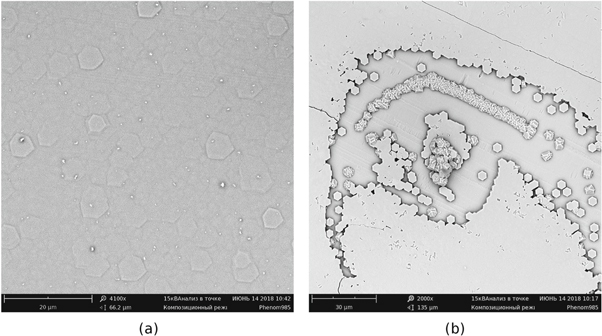
Figure 1. SEM plan view images of Ga2O3 layers on different substrates under similar growth conditions. (a) 1.5 μm α-Ga2O3 layer grown on (0001) sapphire; (b) ε-Ga2O3 layer grown on bulk  β-Ga2O3.
Download figure:
Standard image High-resolution imageThe XRD analysis of the Ga2O3 film on sapphire revealed strong peaks at ∼40.3° and ∼41.8°, corresponding to the (0006) planes of α-Ga2O3 and sapphire, respectively. This confirms that the epitaxial layer is pure α-Ga2O3 polymorph with corundum-like structure. Thus the hexagonal symmetry of islands is not related to the true symmetry of α-Ga2O3 crystal structure and can be explained by the formation of rotation domains. Despite the apparent mosaic structure accompanied with the formation of twin domains, the epitaxial layer exhibits high structural quality with XRC widths of 42 arcsec and 19 arcmin for (0006) and (1018) reflections, respectively.
In contrast, the specimen grown on β-Ga2O3 substrate exhibits strong X-ray diffraction peaks at 2θ = 59.06°, 59.9° and 112.7° corresponding to  (0006) and (00010) reflections of β-Ga2O3 and ε-Ga2O3, respectively. This confirms that the epitaxial layer on bulk β-Ga2O3 is ε-Ga2O3 polymorph with pseudo-hexagonal structure.
Figure 2 shows SEM images of the Ga2O3 layer deposited on 4H-SiC substrate at 500 °C. SEM shows flat surface with hexagonal truncated pyramid-like features assembled in clusters. Regular orientation, uniform size and faceting of these pyramids indicate the epitaxial nature of their formation.
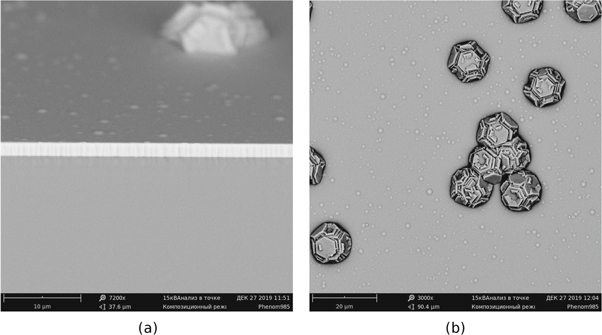
Figure 2. SEM secondary electron image of Ga2O3:Sn layer grown on (0001) 4H-SiC substrate/(a) bird's eye view, (b) plan view.
Download figure:
Standard image High-resolution imageSimilar hexagonal features were also observed on plan view image of Sn-doped Ga2O3 on p-GaN template (Fig. 3). The surface of the specimen has numerous hexagonal plates surrounded by smaller crystallites. These plates are surrounded by smaller size irregular shaped crystallites. Larger hexagonal islands and smaller crystallites emit similar CL spectra with the main broad band centered at about ∼430 nm and ∼410 nm, respectively. Smaller crystallites emit stronger blue band and two additional not well resolved red bands at ∼690 nm and ∼760 nm. Hexagonal islands exhibit a lower integral CL intensity than surrounding areas. Red CL are possibly related to Sn doping because similar bands were observed in Sn-doped β- and α-Ga2O3.31,32
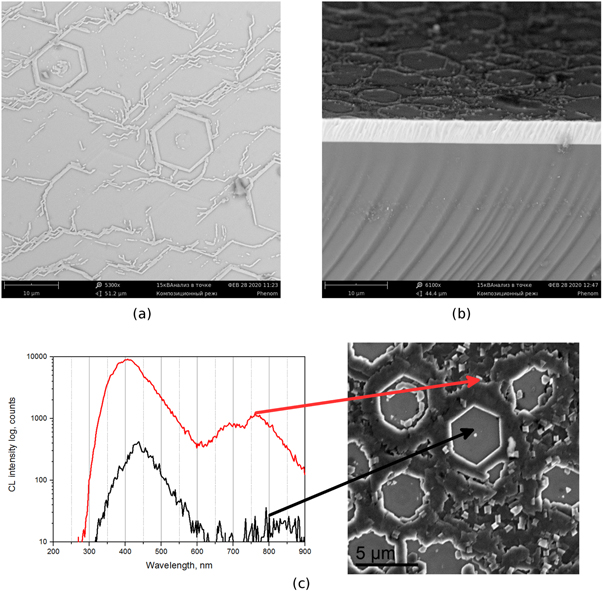
Figure 3. SEM image of Ga2O3 deposited on (0001) p-GaN template (a) plan view back scattered electron image; (b) birds-eyes view; (c) plan view secondary electron image and CL spectra from different regions of the layer.
Download figure:
Standard image High-resolution imageSo far, we have been considering the formation of hexagonal features on planar substrates. The overall picture does not change much for the growth on artificially patterned substrates. We reported previously33 that PSS can be used to control polymorphic composition of Ga2O3 epitaxial layers. Depending on the growth conditions, Ga2O3 deposition on the patterned substrates results in either pure α-Ga2O3, or ε-Ga2O3, or a columnar structure containing both α- and ε-phases. In this work the growth conditions were optimised for the deposition of pure ε-Ga2O3. Figure 4 shows SEM images of the Ga2O3 layer grown on PSS with cone-shape bumps arranged in a hexagonal lattice. As can be seen, Ga2O3 forms regular hexagonal islands on tops of the cones. The structural quality of ε-Ga2O3 layers grown on PSS is higher compared to that for the layers grown on planar substrates (see Table I). Deposition on PSS results in regularly distributed islands of uniform size and shape. In contrast to that, nucleation on planar substrates is more stochastic process and results in randomly distributed islands of various sizes. Consequently, coalescence of regular islands produces less number of grain boundaries and associated defects.
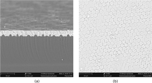
Figure 4. SEM image of ε-Ga2O3 layer grown on patterned sapphire, bird's eye view (a) and plan view (b).
Download figure:
Standard image High-resolution imageNominally undoped Ga2O3 layers were highly resistive. Conducting Ga2O3 films were produced by doping with Sn. The concentration of electrons in the doped specimens was estimated to be in the in the range from low 1017 to high 1019 cm−3. The heterojunctions composed of n-type ε-Ga2O3:Sn and p-type GaN:Mg demonstrated diode-like I-V characteristics. These structures exhibited broad whitish emission under forward bias. It is interesting to note that the electroluminescence (EL) spectrum is evidently different when compared with CL spectra acquired from GaN and Ga2O3 layers of the same structure (Fig. 5). The origin of this phenomenon can be related to the difference in the EL and CL generation regions. The CL emission is generated from nearly the entire layer thickness whereas the EL emission stems from GaN/Ga2O3 interface layer of a thickness of the order of the carrier diffusion length.
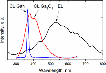
Figure 5. Spectrum of EL emission from ε-Ga2O3/GaN under forward bias. CL spectra from Ga2O3 and GaN layers of the same structure are shown for reference.
Download figure:
Standard image High-resolution imageIt should be mentioned, however, that the electrical conductivity is achieved at the cost of deteriorated crystal quality. Consequently, it is difficult to make an unambiguous conclusion whether the electrical conductivity is related to Sn donors, or associated structural defects, or both. In contradistinction to published studies on Ga2O3 epitaxy,9,23 where Sn acted as a stabilizing agent for the formation of the ε-Ga2O3, we observed a dramatic decrease of the structural quality accompanied with the formation of the competing β-Ga2O3 phase in Sn-doped samples. In some cases Sn doping resulted in polycrystalline texture-like material.
Figure 6 compares XRD ω-2θ scans for Ga2O3 layers grown on sapphire substrate and GaN/sapphire template. For Ga2O3/Al2O3 sample, peaks for the ε-Ga2O3 {0002} set of planes were observed at 19.18°, 38.89°, 59.90°, 83.48° and 112.63°, corresponding to the (0002), (0004), (0006), (0008) and (0, 0, 0, 10) reflections, respectively. Weak peaks at 40.25° and 87.05° correspond to (0006) and (0, 0, 0, 12) reflections of α-Ga2O3. The presence of the small amounts of the α-phase can be explained by the growth of semi-coherent α-Ga2O3 layer on the sapphire substrate, followed by island growth of ε-Ga2O3.
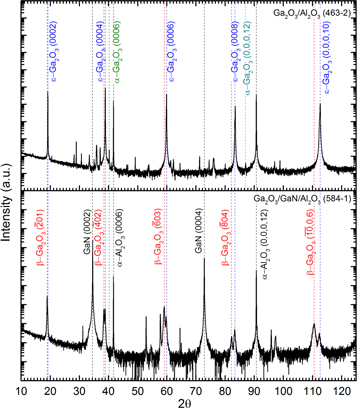
Figure 6. XRD ω-2θ scans of Ga2O3 films on (0001) sapphire substrate (top) (0001) GaN template (bottom).
Download figure:
Standard image High-resolution imageIn addition to ε-Ga2O3 {0002} diffraction peaks, the sample grown on GaN/sapphire template also exhibits diffraction peaks at 18.94°, 38.39°, 59.11°, 82.23°, and 110.52° corresponding to 


 and
and  reflections of β-Ga2O3. The origin of the coexistence of ε and β phases in this specimen could be attributed to heavy Sn doping.
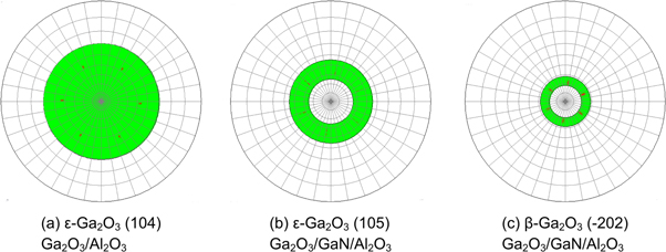
The pole figures of these two Ga2O3 films are shown in Fig. 7. Diffraction spots ε-Ga2O3  and
and  from Ga2O3/Al2O3 Ga2O3/GaN/Al2O3 exhibit expected six fold symmetry (Fig. 7a, 7b). Surprisingly, the pole figure for
  reflection of β-Ga2O3 also shows six-fold symmetry. This indicates that the β-Ga2O3 phase is strongly
  oriented and forms six crystal types of β-Ga2O3 rotated every 60° to each other about this direction. Similar results have been reported by other research groups who observed formation of β-Ga2O3 rotation domains in Ga2O3 epitaxial films on sapphire22,34
Figure 7. X-ray pole figures (log-scale) of (a) ε-Ga2O3 (104), (b) ε-Ga2O3 (105), and (c) β-Ga2O3  phases n Ga2O3 layers grown on various substrates.
Download figure:
Standard image High-resolution image
Conclusions
The present work demonstrates epitaxial growth of ε-Ga2O3 on Al2O3, GaN, SiC β-Ga2O3 and patterned sapphire substrates by the HVPE method. Epitaxial layers of ε-Ga2O3 of comparable quality can be produced on all tested substrates. The narrowest XRC were obtained for the ε-Ga2O3 films grown on patterned sapphire substrates. Most of the samples exhibited islands and other growth features of hexagonal symmetry. However, the sixfold symmetry of the surface feature does not always correlate with the true symmetry of the crystal structure and can be caused by the formation of rotation domains. Doping with Sn resulted in conductive Ga2O3 films; however, the crystalline quality was drastically decreased. Concurrent growth of β-phase was observed in the heavily doped samples. Heterojunctions composed of n-type ε-Ga2O3:Sn and p-type GaN:Mg demonstrated diode-like I-V characteristics and emitted white light under forward bias.
Acknowledgments
The authors would like to acknowledge I.A. Kasatkin for his extensive help with XRD measurements of Ga2O3 layers. V.I. Nikolaev, S.I. Stepanov, A.I. Pechnikov acknowledge support from the Russian Science Foundation, grant no. 19-19-00409.