

Abstract
The performance improvement of PTB7:PC71BM based organic solar cells was achieved and optimized by using a very thin layer of TiO as electron transporting layer (ETL) between the cathode electrode (Al) and active layer of the devices. Different thicknesses of TiO ETL were thermally deposited onto the solution-processed active layers followed by aluminium deposition and device encapsulation under glovebox. Results showed that with the use of 5 nm TiO the power conversion efficiency was improved from 5.6% to 9.63%. This interesting enhancement was attributed to various effects of TiO ETL at the boundary/interface of the semiconductor-metal component. Furthermore, high photosensitivity and fast photo-response for the investigated devices with the presence of TiO indicated their viable use as light photodetector.
Export citation and abstract BibTeX RIS
Since the first emergence of organic solar cell (OSC), great attention has been paid to it with the aim of serving as an alternative to inorganic solar cells. Several importance features are offered by OSCs such as solution processability, flexibility, light-weight, tunability low cost and ease of fabrication.1–4 Organic semiconductors are well known for their unique properties, which can be interestingly employed in various electronic devices such as solar cells, laser diodes, light-emitting diodes and thin-film transistors.5,6
Conjugated polymers and small molecular materials, with high electronic mobility, are the most common candidates to be used in OSCs. A bulk heterojunction (BHJ) blend of P3HT and PC61BM that form the interconnection of donor/acceptor components has been widely used for OSCs fabrication.5,7 OSCs based on fluorinated thieno [3,4-b] thiophene family, the poly[(4,8-bis-(2-ethylhexyloxy)-benzo(1,2-b:4,5-b0) dithiophene)-2,6-diyl-alt-(4-(2ethylhexyl)-3fluorothieno [3,4-b]thiophene-)-2-carboxylate-2-6-diyl)] (PTB7) as an electron donor combined with [6,6]-phenyl C71 butyric acid methyl ester (PC71BM) as electron acceptor have attracted much attention due to their high performance as BHJ solar cells.8–10 PTB7 is a low band gap polymer which possesses significant interest for its use in the bulk heterojunction OSCs as p-type semiconducting polymer. PTB7 based OSC has provided good efficiency due to its extended absorption into the near infra-red and low HOMO level for PTB7 of about 5.15 eV.11–14 [6,6]-Phenyl-C71-butyric acid methyl ester (PC71BM) which is commonly used as n-type semiconductor in OSCs, possesses a strong and broad absorption in the visible range when it is combined with PTB7.2,15 Benefited by these materials properties, the initial donor and acceptor components used in this study are chosen to be PTB7 and PC71BM, respectively.
The charge transport response in OSCs can be improved by means of inserting a hole and electron transporting layers on top of the anode electrode and active layer, respectively. Recently, various hole transport and electron transport layers have been introduced into organic photovoltaic devices in order to achieve a high performance. 2D nanosheet materials have attracted considerable attention as alternatives to PEDOT:PSS owing to their large specific surface area, atomic thickness and tuneable electronic structures.16 For instance, graphene oxide (GO) was used as a potential hole transport layer (HTL) due to its superior electric, optical and mechanical properties.17 In addition, Ti3C2Tx, which is 2D classic representative of the MXenes group, was utilzied as a hole transport layer in polymer solar cells (PSCs) because of its outstanding metallic conductivity, excellent optical transparency, proper work function and superior mechanical properties. It exhibited higher power conversion efficiency (PCE) of 10.53% than that of the pristine ITO-based device (4.21%) with PBDB-T as donor and ITIC as acceptor.18 Furthermore, quinoxaline-phosphine oxide based small molecules (QPSMs) can be used as electron transport layer (ETL) in solution processed OSCs and OLEDs. QPSMs has resulted in simple and effective processing during device fabrication due to the strong dipole moments within their molecular structures when dissolved in alcohol. The introduction of QPSMs as ETL resulted in a significant improvement in Jsc, Voc, FF, and PCE. It has been demonstrated that using QPSMs in OSCs and OLEDs as ETL has led to enhanced electron transport and extraction, which resulted in significantly improved device performance with PCE of 16.83% in the polymer donor:nonfullerene acceptor system and 10.07% in the polymer donor:fullerene acceptor system.19 In the current study, poly(3,4-ethylenedioxythiophene):poly(styrenesulfonate) (PEDOT:PSS) is used as hole transporting layer (HTL). It is solution-processable and its work function acts properly as HTL. Moreover, it has high ability to smoothen the interface between the anode and active layer as well as keeping effective optical transparency in the visible light.20
Chemical degradation of active layer and oxidation of metal electrodes caused by moisture, oxygen and/or light and phase separation of organic blends are the most commonly factors that lead to degradation of OSCs.21 An efficient strategy used to overcome these obstacles and to improve the OSCs performance is to insert an interfacial layer between the active layer and the electrodes in both of conventional OSCs and inverted ones.1 Also, this strategy acts upon improving the junction conductivity, thereby increasing charge transportation. Consequently, there would be a good chance to decrease the charge recombination process and hence improving the light absorption and photocurrent.22 Devices made of PTB7:PC71BM demonstrated a power conversion efficiency (PCE) of 9.2% when poly [(9,9-bis(3'-(N,N-dimethylamino)propyl)-2,7-fluorene)-alt-2,7-(9,9–dioctylfluorene)] (PFN) was used as surface modifier between the ITO electrode and active layer in an inverted structure.11 This is where the conventional device structure showed an average PCE of 8.37% when Poly [(9,9-bis(3'-(N,N-dimethylamino)propyl)-2,7-fluorene)-alt-2,7-(9,9–dioctylfluorene)] (PFN) was used as interlayer between the active layer and Al electrode.23
Some materials like metal oxides, conjugated polyelectrolytes (CPEs), and self-assembled monolayers (SAMs) can support electrons transportation between active layer and cathode and consequently enhance the photovoltaic device performance when they are utilized as interfacial materials.24 Recently, a special attention has been paid to titanium dioxide (TiO2) films due to their attractive photocatalytic properties and excellent chemical, optical and electrical properties.25 TiO2 was successfully used in dye-sensitized cells and hybrid polymer/TiO2 cells with the capability of showing high absorption coefficient,26 high electron mobility, environmentally friendly material with comparatively low price and excellent chemical and physical stability.27 TiO2 can be considered as a promising candidate as electron acceptor (n-type semiconductor) and electron transport material. Moreover, by the use of few nanometres thick of TiO2 as electron transport layer (ETL), electron–hole recombination as well as direct contact between the active layer and the cathode layer can be avoided. The TiO2 ETL is acting as electron extractor at the active layer/TiO2 interface and as electron transporter in the planar structured devices.28 As choosing the right thickness of ETL plays a crucial role in the performance of OSCs, finding the optimum thickness, either for the active layer or ETL layer, thereby achieving strong absorption with efficient charge carrier collection, is considered as a current challenge in OSCs. Therefore, this work is devoted to study the rate of improvement in the overall performance of PTB7:PC71BM based OSCs by means of using TiO2 as ETL. In this way, the active layer and ETL thicknesses are first optimized by fabricating several devices with different active layer thicknesses without the inclusion of ETL. Then, the one with the best PCE is chosen to be improved through the addition of TiO2 based ETL with different thicknesses.
Materials and Methods
PTB7 and PC71BM (95/5%) were purchased from Ossila and used as received. These chemicals serve as electron donor (D) and acceptor (A), respectively. Titanium dioxide nano-powder, with average particle size of 20 nm, was purchased from Sigma-Aldrich. The ITO pattered glass substrates with resistance of 5 Ω were purchased from Luminescence Technology Crop. Poly(3,4-ethylenedioxythiophene):poly(styrenesulfonate) (PEDOT:PSS) CLEVIOS™ PH 1000 was purchased from Heraeus Deutschland GmbH & Co. KG. The molecular structures of PTB7 and PC71BM are shown in Fig. 1.
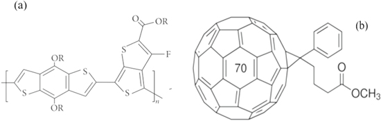
Figure 1. The molecular structures of (a) PTB7 and (b) Fullerene PC71BM.
Download figure:
Standard image High-resolution imagePTB7:PC71BM solution with weight ratio of (1:1.5) and concentration of 20 mg.ml−1 was prepared in chlorobenzene (CB). This weight ratio was chosen since it showed the highest PCE among other ratios.12,29 After that, the solution was stirred in amber vial for about 48 h using magnetic stirrer in order to allow homogeneity and inter-dispersion of the molecules.
It is known that there is a limit on the selection of active layer thickness for optimum OSC performance. One of the most important parameters that can control the active layer thickness is the spin coating speed. Therefore, before the solar cell devices were fabricated, the PTB7:PC71BM blend was spin coated on a glass substrate at a speed of 700, 1000, and 1500 rpm in order to realize different thicknesses. The thicknesses were confirmed to be 100, 80 and 70 nm for the 700, 1000, and 1500 rpm, respectively, by using the profilometer of DEKTAK 8000 KLA Tencor P-6. UV–vis-NIR spectroscopy (Ocean Optic, USB4000) was used to record the optical absorption of the films. The photoluminescence (PL) measurements of PTB7, PC71BM and PTB7:PC71BM films were carried out using Perkin Elmer LS55 fluorescence spectrometer. Incident photon conversion efficiency (IPCE) measurement was performed using IPCE measurement system (Newport Co., ORIEL LCS—100TM).
The organic solar cell devices were fabricated on patterned ITO-coated glass substrate. The ITO substrates were precleared by ultrasonic bath in detergent, deionized water, Isopropyl Alcohol (IPA), acetone and deionized water sequentially for 20 min. All cleaning stages were performed under the same conditions of cleaning and time duration. Then, the substrates were dried by blowing nitrogen gas. After that, oxygen plasma treatment was applied to the ITO substrates for 5 min before the hole transport layer is spin coated in order to remove any foreign contaminants present on the surface of the substrate and making it more suitable for further coating process. Shortly after the plasma cleaning, PEDOT:PSS was coated over ITO substrate at 3000 rpm for 60 s to fulfill efficient hole transportation and also to smoothen the surface of the ITO, followed by its annealing at 120 °C for 30 min. The thickness of PEDOT:PSS was fixed at about 40 nm. Afterwards, active layer composed of PTB7:PC71BM blends was coated over the PEDOT:PSS layer with thickness of 70, 80 and 100 nm, respectively.
The samples and the coating process were prepared in oxygen and moisture free nitrogen atmosphere inside the glove box. Next, the samples were loaded into the vacuum chamber, which is located in the same glovebox for the deposition of Al electrode. Thereafter, Al electrode (100 nm) was deposited by thermal evaporation through a shadow mask under a pressure of 10−4 Pa to obtain a device with an active area of 0.045 cm2. Finally, all the fabricated devices were encapsulated by using a glass substrate on the top of the devices to avoid the degradation on the cell performance caused by the penetration of moisture and oxygen into the active layer. The schematic of fabricated OSC with architecture of ITO/PEDOT:PSS/PTB7:PC71BM/Al and energy level diagram of the materials used for OSC fabrication are presented in Fig. 2.
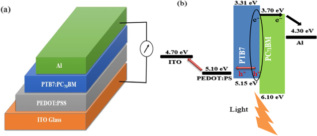
Figure 2. (a) Schematic of the fabricated OSC based on PTB7:PC71BM active layer and (b) Energy level diagram of the materials used for OSC fabrication.2
Download figure:
Standard image High-resolution imageLater, the three devices with different active layer thicknesses went through current–voltage (I–V) measurements in order to determine the best active layer thickness. The (I–V) measurements were performed using a Keithley 236 instrument under 80 mW.cm−2 illumination from an Oriel solar simulator-model 67005 with an AM 1.5 G filter under ambient condition. The optimum active layer, by which the best (I–V) performance was achieved was used to fabricate another batch of solar cells with the addition of TiO2 ETL. The deposition of TiO2 was performed inside a vacuum chamber through a shadow mask under a pressure of 10−4 Pa. TiO2 layer thickness was carefully controlled by using a high vacuum thermal deposition system (PVD) in order to obtain a thickness of 1, 5 and 10 nm, respectively. This variation on TiO2 thickness was performed in order to realize the best PCE among them. Afterwards, Al electrode (100 nm) was thermally deposited under the same condition. Finally, encapsulation process was performed in order to avoid the degradation on the cell performance caused by moisture and oxygen. The schematic of fabricated OSC with architecture of ITO/PEDOT:PSS/PTB7:PC71BM/TiO2/Al and energy level diagram of the materials used for OSC fabrication are presented in Fig. 3. It is worth to mention that based on the results from literature,30 the TiO2 structure is decomposed into the more stable form of titanium oxide (TiO) at high temperature of above 400 °C and under high vacuum. Hence, the deposited ETL layer in the current work is assigned to TiO.
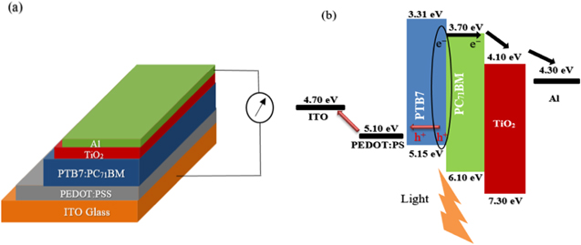
Figure 3. (a) Schematic of the fabricated OSC based on PTB7:PC71BM active layer with introduction of TiO ETL and (b) energy level diagram of the materials used for OSC fabrication.
Download figure:
Standard image High-resolution imageResults and Discussion
Figure 4 shows the absorption spectra of PTB7, PC71BM and bulk heterojunction of PTB7:PC71BM thin films, respectively. The absorption band of the PTB7 film extended over the wavelength range from 550 to 750 nm, which can be considered as a strong light absorbing agent, whilst PC71BM absorbs in the wavelength range from 300 to 500 nm. These results are very close to those reported in literature for both of the components.15 The peaks at 620 nm and 662 nm are noticed to be the highest absorption peaks in the PTB7 spectrum, which are attributed to the characteristic π−π* transition,12 whereas peaks at 380 nm and 475 nm with a shoulder at 570 nm are observed in the PC71BM spectrum. As observed in Fig. 4a, PC71BM which possesses a strong absorption in the UV as well as in the visible region was used as an acceptor in the PTB7:PC71BM blend to recompense the PTB7 absorption in these regions. A wide range from the UV region to about 800 nm wavelength, which is considered as the main portion of the solar spectrum, was covered by the absorption spectrum of PTB7:PC71BM blend as a result of its components overlapping. Moreover, it can be clearly noticed that there is a red shift in the absorption spectrum of the PTB7:PC71BM blend compared to that of the pristine PTB7. The first peak was shifted from 620 nm on PTB7 spectrum to 625 nm on PTB7:PC71BM spectrum, and the second peak from 662 nm on PTB7 to 677 nm on PTB7:PC71BM. The presence of a red shift in the absorption spectra of PTB7:PC71BM film with respect to that of the PTB7 film is ascribed to the enhanced photo-induced charge transfer between the donor and acceptor moieties.31 This red shift is considered to be one of the main strategies towards improving the performance of OSCs due to enhanced capture of photons by the active layer.
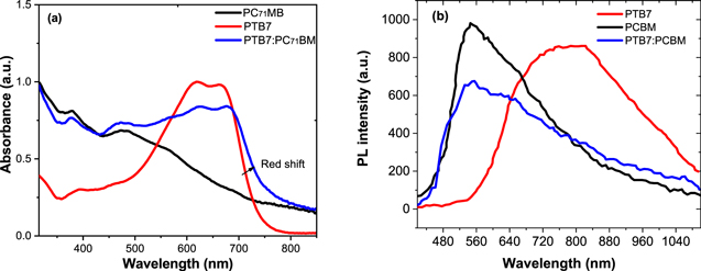
Figure 4. (a) Absorption spectra and (b) Photoluminescence spectra of PTB7, PC71BM and PTB7:PC71BM films.
Download figure:
Standard image High-resolution imageFigure 4b shows the photoluminescence (PL) spectra of PTB7, PC71BM and PTB7:PC71BM (1:1.5) thin films recorded at excitation wavelength of 400 nm. The PL peak of PTB7 and PC71BM thin films was found to be at 790 and 546 nm, respectively, which is consistent with that reported in literature.32 One can notice that the PL of PTB7:PC71BM composite has undergone a quenching phenomena compared to that of the pristine PTB7, indicating the occurrence of a useful photo-induced charge transfer for photovoltaic applications. Upon the incorporation of PC71BM into the PTB7, a strong optical coupling is taken place between the D-A moieties, resulting in a decreased radiative recombination in the blends. Taking into account the charge transfer (CT) energy state at the corresponding PL peak of the blend, it was estimated that the CT energy is about 1.5 eV. Noteworthy, the energy state of CT is about 0.8 eV higher than qVoc, where Voc is the open circuit voltage of the measured solar cells.
The device architecture used in the first part of this study is ITO/PEDOT:PSS/PTB7:PC71BM/Al. Various active layer thicknesses of PTB7:PC71BM BHJ blend were used to verify thickness influence on the device performance. Figure 5 shows the current density-voltage (J–V) characteristics and maximum power density of the devices under illumination. Table I lists the photovoltaic parameters of the devices, which include circuit current density (JSC), open circuit voltage (VOC), fill factor (FF) and power conversion efficiency (PCE), while Table II presents the electrical parameters of the devices that were extracted using the single-diode modelling approaches.33,34 The electrical parameters of the devices are ideality factor (n), series resistance (Rs), shunt resistance (Rsh), saturation current (Io) and photocurrent (Iph).
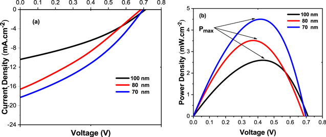
Figure 5. Photovoltaic performance of the binary devices based on PTB7:PC71BM blend of different thicknesses; (a) Current density–voltage (J−V) characteristic and (b) Power density−voltage (P−V) characteristics.
Download figure:
Standard image High-resolution imageTable I. Photovoltaic parameters of BHJ solar cells based on PTB7:PC71BM composite with different active layer thicknesses.
| PTB7:PC71BM Thickness (nm) | Jsc (mA.cm−2) | Voc (V) | FF (%) | PCE (%) |
|---|---|---|---|---|
| 100 | 10.39 | 0.71 | 35 | 3.26 |
| 80 | 16.57 | 0.69 | 30 | 4.41 |
| 70 | 18.30 | 0.70 | 35.2 | 5.63 |
Table II. The calculated electrical parameters of BHJ solar cells based on PTB7:PC71BM composite with different active layer thicknesses.
| PTB7:PC71BM Thickness (nm) | n | Rs (Ω.cm2) | Rsh (Ω.cm2) | Iph (A) | Io (A) | RMSE |
|---|---|---|---|---|---|---|
| 100 | 4.27 | 18.11 | 108.43 | 12.1E-3 | 9.4E-6 | 4.7E-5 |
| 80 | 2.04 | 16.27 | 40.79 | 23.1E-3 | 3.9E-8 | 6.1E-4 |
| 70 | 4.02 | 10.14 | 58.91 | 21.6E-3 | 1.2E-5 | 3.8E-5 |
Table I and Fig. 5 show a significant effect of the active layer thickness on the device's performance. The OSC device with 100 nm active layer showed open circuit voltage (VOC), short circuit current density (JSC), fill factor (FF) and PCE of 0.7 V, 10.4 mA.cm−2, 35%, and 3.22%, respectively. When the thickness was decreased to 80 nm, the VOC retained the same value of 0.7 V, while a significant increase in the JSC was achieved to 16.6 mA.cm−2. Whilst the FF dropped from 35% to 30%, the PCE increased by 35% to accomplish 4.35%. Since the devices were fabricated under the same condition of final electrode deposition, the decrease in FF for the devices of 80 nm active layer compared to that of 70 nm might be due to increased charge carrier recombination and reduced diffusion length of excitons before their dissociation at the donor-acceptor boundaries. Further decrement in thickness from 80 to 70 nm, has led to increase the JSC and FF to 18.3 mA.cm−2 and 35.2%, respectively.
In order to elaborate on the reasons of relatively low value of FF, the experimental J–V data were fitted to the well-known single diode equation used for solar cells simulation and hence the electrical parameters of the devices were calculated accordingly,33–35 as shown in Table II. The small value of root mean square error (RMSE) between the measured and calculated currents justifying the reliability of the theoretical model to extract the parameters accurately. It was reported that if the series resistance of OSCs is reduced to 0.1 Ω.cm2 the FF can be maximized to 60%, while FF of the device is reduced to 52% with the Rs of about 6.2 Ω.cm2.36 Furthermore, enlarging Rs to 10 Ω.cm2 has led to an obvious loss of FF and efficiency while the JSC and VOC remained unchanged. Comparably, the Rs of our devices shown in Table II is more than 10 Ω.cm2, implying a negative effect of Rs on the FF. Moreover, it was found in literature that if Rsh is larger than 6 kΩ.cm2, the effect of Rsh on FF is negligible.36 As can be seen, the highest Rsh recorded for our devices is in the rage of 100 Ω.cm2. Therefore, the low FF in the studied solar cells are reasonably due to the high and low values of Rs and Rsh, respectively. These imperfect parasitic resistances are also resulted in the mismatch of holes and electrons mobility.
It was reported in literature that the optimum thickness of the active layers, in terms of light absorption and charge transport response, can be in the range of 80−120 nm.37 Comparably, a thinner active layer acts upon improving the charge transport properties at the expense of light absorption and overall efficiency. Therefore, we chose the active layer thickness to be about 70 nm. Consequently, the next batch of devices were decided to fabricate at active layers of 70 nm thickness. The observed improvement in the PCE when thickness of the PTB7:PC71BM active layer was decreased can be due to three reasons. First, the smaller thickness is lead to decreased charge traps and hence less recombination rate of holes and electrons are resulted. Second, with a smaller thickness there would be a shorter pathway for the charge carriers to travel reaching their corresponding electrodes, thereby reducing the limitations of short diffusion length for the electrons and holes in the devices active layer. Third, it can be due to enhanced built-in electric field across the active layer, which is caused by the reduction of the active layer.
The device architecture used in the second part of this study is ITO/PEDOT:PSS/PTB7:PC71BM/TiO2/Al. Different TiO layer thicknesses were used to verify its influence on the device efficiency. Figure 6 shows the J–V characteristics and the maximum power density of the devices with TiO ETL of different thicknesses under illumination. Table III lists the variation in the photovoltaic parameters of the devices upon the inclusion of TiO ETL, while Table IV presents the extracted electrical parameters of the devices incorporating different TiO thicknesses.
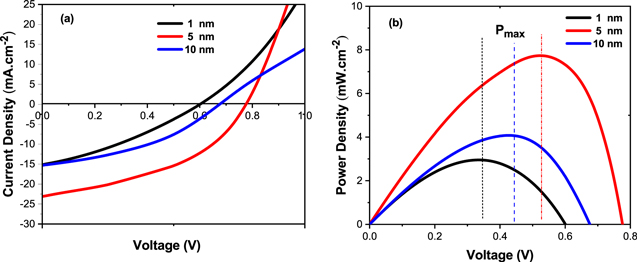
Figure 6. Photovoltaic performance of the devices based on PTB7:PC71BM blend with the introduction of different ETL thicknesses of TiO; (a) Current density–voltage (J−V) characteristic and (b) Power density−voltage (P−V) characteristics.
Download figure:
Standard image High-resolution imageTable III. Photovoltaic parameters of solar cell based on PTB7:PC71BM composite with introduction of different ETL thickness of TiO2.
| TiO Thickness (nm) | Jsc ( mA.cm−2) | Voc (V) | FF (%) | Avg. PCE (%) | Best PCE (%) |
|---|---|---|---|---|---|
| 1 | 13.34 ± 1.5 | 0.66 ± 0.07 | 31.5 ± 2.3 | 3.43 ± 0.2 | 3.6 |
| 5 | 21.34 ± 1.3 | 0.79 ± 6.23E-3 | 44.8 ± 1.8 | 9.39 ± 0.17 | 9.63 |
| 10 | 15.1 ± 0.29 | 0.66 ± 0.01 | 37.8 ± 2.5 | 4.76 ± 0.37 | 5.05 |
Standard deviation was considered amid five measured devices.
Table IV. The calculated electrical parameters parameters of solar cell based on PTB7:PC71BM composite with introduction of different ETL thickness of TiO2.
| TiO Thickness (nm) | n | Rs (Ω.cm2) | Rsh (Ω.cm2) | Iph (A) | Io (A) | RMSE |
|---|---|---|---|---|---|---|
| 1 | 1.03 | 18.67 | 39.74 | 22.6E-3 | 5.3E-12 | 8.9E-4 |
| 5 | 5.02 | 7.39 | 132.07 | 16.3E-3 | 6.1E-5 | 1.4E-4 |
| 10 | 5.48 | 0.14 | 84.09 | 23.6E-3 | 6.1E-5 | 2.9E-4 |
Table II and Fig. 6a illustrates the presence of a significant effect on the device performance by the addition of different TiO ETL thicknesses. The OSC device with 1 nm thick TiO ETL showed a PCE of 3.6%, VOC of 0.6 V, JSC of 15.2 mA.cm−2 and FF of 31.6%. After TiO thickness has been increased to 5 nm, a surprised performance was achieved, revealing a very high improvement on the J–V device parameters. The JSC was increased by 26% to reach the value of 23.1 mA.cm−2, which plays a critical role in improving the device performance. The device also shows an enhancement in the VOC and FF to be 0.77 V and 43%, respectively. Moreover, an interesting high PCE value of 9.63% was achieved, which is considered as the highest PCE that has been reported for the OSC based on binary blend of PTB7:PC71BM. Noteworthy, devices with 5 nm TiO performed excellent raise in the PCE by 71.8% to accomplish 9.63% compared to the device without TiO which has achieved the best PCE of 5.6%. Nevertheless, a device with 10 nm thick TiO layer exhibited a decline in the values of JSC, VOC, FF and PCE to 15.3 mA.cm−2, 0.67 V, 39% and 5.05%, respectively. We anticipate that the relatively low FF for our devices can be due to the high and low values of Rs and Rsh, respectively, as was discussed before. This ultimately leads to an unbalanced mobility of electrons and holes along with increased charge recombination.35,37
The higher PCE of the PTB7:PC71BM/TiO (5 nm) device is attributed to the effective charge dissociation and transport across the p-n junctions of the active layer. The effective charge dissociation and transport can be ruled by the changes in IPCE and generated maximum power by the solar cells, as shown in Figs. 6b and 8b, respectively. It was observed that the device with 5 nm TiO thickness showed the highest power density and IPCE compared to the other devices, pointing out to the occurrence of efficient photon to electron conversion process. Moreover, the thermally deposited TiO layer has the ability to work as a charge relay component and it shows a cascade energy level with PTB7 and PC71BM as shown in Fig. 3b. Due to the well-matched energy between TiO conduction band (4.1 eV)15 and Al work function Al (4.3 eV), electrons can easily move from PC71BM (LUMO level: 3.7 eV) to Al.2 On contrary, the valence band (7.3 eV) of TiO which is higher than the highest-occupied molecular orbital (HOMO) level of PTB7 (5.15 eV), hinders the accumulation of the holes at the active layer-(Al) cathode interface, which results in the reduction of interfacial charge recombination. Furthermore, the use of TiO as a buffer layer (ETL) can lead to improve the photon harvesting by redistributing the light intensity in the blend film. The decline in the device performance of 10 nm TiO thickness is attributed to the increase in the charge recombination, whereas the charge carriers are travelling a longer path to reach the Al electrode and hence present a profound impact on the JSC and VOC. For more elucidation on the effect of TiO ETL thickness on the photovoltaic performance, Fig. 7 shows variation in the photovoltaic parameters of the devices with different TiO thicknesses. This change showed almost a symmetric tend around the highest values of JSC, VOC, FF and PCE for the devices with 1 nm, 5 nm and 10 nm TiO layer thickness, respectively.
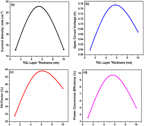
Figure 7. Variation in the photovoltaic parameters of the devices with different TiO ETL thicknesses.
Download figure:
Standard image High-resolution imageThe P–V characteristics of the organic solar cells based on PTB7:PC71BM and PTB7:PC71PM/TiO are shown in Figs. 5b and 6b, respectively. The maximum power of the solar cell is known as the highest power value that can be delivered to the external load. This power can be obtained only when both the internal resistance of the cell and the load resistance are equal.38 For the devices with various PTB7:PC71BM active layer thickness of 100, 80 and 70 nm, the maximum power is found to be 2.6, 3.5 and 4.5 mW.cm−2, respectively. It's noticeable that the increase in the maximum power, produced by the cells, follows the same behaviour of its IPCE response. After adding TiO ETL, the generated maximum power has increased from 4.5 mW.cm−2, which represent the best for PTB7:PC71BM active layer, to 7.7 mW.cm−2 for the 5 nm TiO thickness which is considered as the best value. Moreover, the maximum power generated by the cells with different TiO thickness which are 2.9, 7.7 and 4 mW.cm−2 for 1, 5 and 10 nm, respectively, is consistent with the increase in PCE.
IPCE suggests the capability of the conversion efficiency of the incident photons into charge carriers at the external circuit. IPCE response of the OSC devices with different PTB7:PC71BM active layer thicknesses are shown in Fig. 8a. IPCE spectra as well as the absorption spectra of the PTB7:PC71BM blend share a similar behaviour, demonstrating that the absorption wavelengths from 400 to 800 nm are all contributing in the photocurrent. It is worth to mention that the IPCE response of the PTB7:PC71BM based solar cells is symmetric with its PCE behaviour. The device with 70 nm active layer thickness has achieved the highest IPCE response as 50%. It can be noticed that with further increase in the active layer thickness to 80 and 100 nm, the IPCE response decreases, suggesting that thicker layers increase carrier recombination and reduce the number of extracted charge carriers.
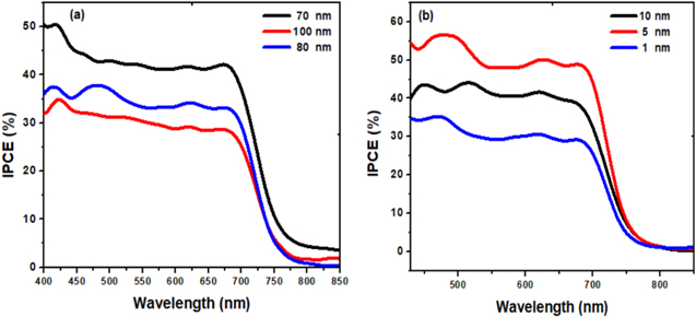
Figure 8. IPCE spectra of organic solar cells based on (a) PTB7:PC71BM blend of different thickness. (b) PTB7:PC71BM blend with addition of different thickness of TiO ETL.
Download figure:
Standard image High-resolution imageFigure 8b shows the IPCE spectra after the insertion of the TiO layer. An improvement in the IPCE is observed after adding the TiO2. This improvement with TiO layer supports the role of TiO as ETL, which enhances the charge transport and extraction to the external circuit. The device with 70 nm active layer thickness and 5 nm TiO layer has achieved the highest IPCE response as 57%, pointing to an effective photon to electron conversion process.
Various optical technologies like building both sources as light emitting diodes (OLEDs) and sensing system as organic photodetectors (OPDs), make good use of solution-processed semiconducting polymers and small-molecules.39 Recently, PTB7:PC71BM bulk-heterojunction active layer has been used to fabricate two sets of organic photodetectors with inverted and conventional structures. The results indicated that the inverted structure showed higher responsivity behavior than the conventional one.40 These results draw our attention to investigate the capability of the conventional structure device, based on solution processed PTB7:PC71BM BHJ with and without TiO ETL, to be used as organic photodetector.
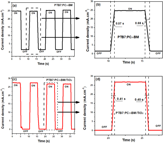
The current density of the organic based photodetector as a function of time was recoded under 80 mA.cm−2 light illumination, as shown in Fig. 9. The performance of the OSC devices as a photodetector can be elucidated by the photo-response and the photosensitivity's value [(Jlight − Jdark)/Jdark].41 The organic based photodetector with TiO recorded very high photosensitivity compared to that without TiO, reporting an increase of 7.6 times, from 15.3 to 116.3. The photo-response speed, which is characterized by the rise time (τr) and fall time (τf) of a transient photocurrent response to an optical signal, is defined as the period of time of the photocurrent to reach 90% of its maximum value and declining to 10%, respectively.42
Figure 9. Photocurrent as a function of time as obtained by switching on and off 80 mA.cm−2 light illumination on the organic photodetector based on PTB7:PC71BM with and with out TiO ETL at a bias voltage of −1 V.
Download figure:
Standard image High-resolution image
The jump and the fall back, by the same amount of current density, during repetitive switching of light illuminations for both devices indicating high sensitivity and stability of the devices. Both devices with and without TiO exhibited rise and fall times which are less than 1 s, as shown in Figs. 9b and 9d, demonstrating a fast photocurrent response. Higher photosensitivity and faster photo-response for the device with 5 nm of TiO indicates its capability for being used as a light photodetector, which has been reported for the first time in this study.
Conclusions
In this study, we demonstrated a significant improvement in device performance of OSC by the inclusion of TiO as ETL via thermal evaporation method. The results revealed that the OSC based on PTB7:PC71BM with 70 nm thickness showed the best PCE of 5.6%. Moreover, an enhancement on the PCE which was resulted after the inclusion of 5 nm TiO2 ETL, showed a PCE of 9.63% as the highest PCE reported to date for the conventional OSC based on the binary PTB7:PC71BM blend. Moreover, IPCE of the solar cells was measured and the best efficiency was found to be 50% and 57% for the devices with 70 nm PTB7:PC71BM layer thickness and with 5 nm TiO layer thickness, respectively. Finally, it was concluded that devices with 5 nm TiO layer thickness has the ability for being used as a light photodetector due to its high photosensitivity and fast photo-response. Our results are a good indication that with the use of TiO buffer layer as the interface of the top-electrode and active layer, with the help of a cheap and easy deposition approach, it is possible to, provide affordable photovoltaic performance and photodetector response.
Acknowledgments
Authors would like to thank the Low Dimensional Materials Research Centre (LDMRC), Universiti Malaya and Micro-Nano System Engineering Lab, Universiti Teknologi Malaysia for facilitating the instruments while carrying out the experiments. Fahmi F. Muhammadsharif is thankful to the Islamic Development Bankfor their support under IDB Merit Scholarship Program.