
Abstract
The development of anodic films at a constant current density of 10 mA cm−2 has been studied for Mg-W alloys, containing 0.4 and 1.0 atom % W, in 3 M ammonium hydroxide/0.05 M ammonium phosphate electrolyte at 293 K. The structure, morphology, and composition of the films were determined by X-ray diffraction, scanning electron microscopy, atomic force microscopy, glow discharge optical emission spectroscopy, Rutherford backscattering spectroscopy, and nuclear reaction analysis. During anodizing to about 50 V, a relatively smooth film develops. Cross-sectional atomic force microscopy suggests the film may be finely porous. With an increase in voltage, the film transforms gradually to a coarse, porous morphology due to dielectric breakdown. The transformation coincides with a reduction in slope of the voltage-time response. Significant regions of both types of film morphology coexist during anodizing to 150 V. With further anodizing, a porous film, developed in the presence of sparking above about 270 V, eventually covers all of the macroscopic surface. Magnesium, phosphorus, oxygen, hydrogen, and nitrogen species are present throughout the film thickness at the resolution of the measurements. However, the films are initially free of tungsten species due to enrichment of tungsten in the alloy. The O:Mg atomic ratio is in the range 1.7 to 2.1, reducing with an increase in voltage for films formed up to 220 V, consistent with films composed primarily of hydroxide or oxyhydroxide. The P:O atomic ratio increases with an increase in voltage, starting at about 0.03 for voltages below 50 V and reaching 0.29 at 330 V. The films form at a reduced efficiency, typically about 40-50%. © 2001 The Electrochemical Society. All rights reserved.
Export citation and abstract BibTeX RIS
Magnesium and magnesium alloys can be used in many applications without protective coatings.1 However, coatings are necessary to provide both corrosion and wear resistance in aggressive conditions. The coatings include anodic films that can often withstand more demanding environments. However, the anodic films on magnesium are poorly understood compared with those on aluminum, tantalum, and other valve metals. Aluminum in particular has attracted wide-ranging studies of anodizing behavior due to the commercial importance of its alloys. In contrast, magnesium usage is comparatively low, although magnesium markets are expanding due to the demand for light materials. Thus, surface treatment of magnesium is of continuing relevance.
The two most favored anodizing processes for magnesium alloys, namely, HAE2 and DOW17,3 rely on sparking on the anode to develop ceramic-like films. However, there are numerous other proprietary processes for anodizing light alloys that involve sparking, which have not been adopted on a large scale (see, for example, Ref. 4 5 6 7 8 9). The resultant films, typically of thickness up to tens of micrometers, are porous and sealing is often necessary to impart high corrosion resistance. Sparking processes can also develop films that contain various crystalline constituents of high hardness, thus providing enhanced tribological properties.10 11 Many proprietary processes also exist that do not rely on sparking (see, for example, Ref. 12 13 14 15).
Studies of films on magnesium formed below the voltage for dielectric breakdown are few compared with those of barrier films on aluminum and tantalum. In general, amorphous anodic oxides, such as anodic alumina and anodic tantala, grow by counter migration of cations and  ions through the film by a short-range mechanism that conserves ionic order.16
17
18 New oxide forms at both the metal/film and film/electrolyte interfaces. In contrast, crystalline films, such as anodic zirconia and anodic hafnia, form primarily by transport of oxygen species, involving short-circuit paths.19
20 Hence, the new oxide grows largely at the metal/film interface. In the case of alumina films, field-assisted ejection of cations and field-assisted dissolution of alumina, which occur in electrolytes that are more reactive to the alumina, lead to growth of porous films consisting of approximately hexagonal cells with a central pore orientated normal to the metal/film interface. A barrier layer is present next to the metal, i.e., at the base of each cell, which remains of constant thickness during steady-state growth.
ions through the film by a short-range mechanism that conserves ionic order.16
17
18 New oxide forms at both the metal/film and film/electrolyte interfaces. In contrast, crystalline films, such as anodic zirconia and anodic hafnia, form primarily by transport of oxygen species, involving short-circuit paths.19
20 Hence, the new oxide grows largely at the metal/film interface. In the case of alumina films, field-assisted ejection of cations and field-assisted dissolution of alumina, which occur in electrolytes that are more reactive to the alumina, lead to growth of porous films consisting of approximately hexagonal cells with a central pore orientated normal to the metal/film interface. A barrier layer is present next to the metal, i.e., at the base of each cell, which remains of constant thickness during steady-state growth.
Studies of film growth on magnesium at constant current density in a  bath at room temperature revealed linear voltage-time responses until dielectric breakdown.21
22 Dielectric breakdown, which started at about 50 V, was accompanied by voltage oscillations, sparking, and evolution of oxygen. Prior to breakdown, a passive film formed on the metal under a high electric field. Potentiostatic polarization resulted in passive behavior to about 4 V, active behavior with pitting and oxygen evolution to about 10 V, secondary passivity to about 60 V, and unstable transpassivity at higher voltages. Secondary passivity has been attributed to formation of MgO.23
24 The current density in the region of secondary passivity reduces with addition of aluminum to the magnesium or of aluminate to the electrolyte.21
22
bath at room temperature revealed linear voltage-time responses until dielectric breakdown.21
22 Dielectric breakdown, which started at about 50 V, was accompanied by voltage oscillations, sparking, and evolution of oxygen. Prior to breakdown, a passive film formed on the metal under a high electric field. Potentiostatic polarization resulted in passive behavior to about 4 V, active behavior with pitting and oxygen evolution to about 10 V, secondary passivity to about 60 V, and unstable transpassivity at higher voltages. Secondary passivity has been attributed to formation of MgO.23
24 The current density in the region of secondary passivity reduces with addition of aluminum to the magnesium or of aluminate to the electrolyte.21
22
Transmission electron microscopy (TEM) of films formed on magnesium in acidic, fluoride-containing electrolyte has disclosed a porous film morphology,25 reminiscent of the cellular morphology of porous alumina films.26 The barrier layer thickness indicated an electric field of about  compared with about
  for anodic alumina.27 The films consisted of both amorphous material, primarily magnesium oxyhydroxide, and crystalline material, namely,
  and
and  the latter developing in the porous region where the electric field is low.25
The present study examines the anodic films formed on dilute Mg-W alloys in an alkaline phosphate electrolyte. These alloys were chosen specifically as model systems with tungsten facilitating the investigation of enrichment of alloying elements in magnesium alloys during anodic oxidation. The tungsten, of high mass relative to magnesium, can be readily detected by Rutherford backscattering spectroscopy (RBS), while the low additions limit any other influences of tungsten on the films during anodizing. Essentially similar enrichment is anticipated with certain alloying elements of commercial magnesium alloys, such as copper and manganese, although the sensitivity of RBS for detection of these is reduced. The enrichment of tungsten during anodizing has been reported separately.28 Briefly, the formation of the anodic film leads to enrichment of tungsten in the alloy to at least  The findings suggest a similarity with that of alloying elements in aluminum alloys.29 Here, the particular interest is in the composition, morphology, and structure of films developed during anodizing to about 300 V.
Experimental
Two dilute Mg-W alloys, containing 0.4 and 1.0 atom % W, were prepared by magnetron sputtering. The alloys were deposited as layers, about 800 nm thick, onto aluminum substrates, which had been either electropolished or electropolished and anodized to achieve flat surfaces. The films on the anodized substrates were barrier-type formed in ammonium pentaborate electrolyte. The deposition was carried out in an Atom Tech system, using separate targets of 99.9% magnesium and 99.95% tungsten. The chamber was evacuated to  with layers deposited subsequently in
  argon of purity 99.998%. Following masking with lacquer, the alloys were anodized individually at 10 mA cm−2 in 3 M ammonium hydroxide
  ammonium phosphate
  electrolyte (pH 10.7) at 293 K. The anodizing conditions correspond to those of the Anomag process.30
31 Films were formed to a range of voltages. Anodizing was terminated immediately when the selected voltage was achieved, and the specimen was removed quickly from the electrolyte, rinsed briefly in deionized water, and dried with a cool stream of air. The voltage-time response was recorded during anodizing of each specimen.
electrolyte (pH 10.7) at 293 K. The anodizing conditions correspond to those of the Anomag process.30
31 Films were formed to a range of voltages. Anodizing was terminated immediately when the selected voltage was achieved, and the specimen was removed quickly from the electrolyte, rinsed briefly in deionized water, and dried with a cool stream of air. The voltage-time response was recorded during anodizing of each specimen.
The structures of alloys and films were determined by X-ray diffraction (XRD) using a Philips  instrument, with radiation from a copper anode. The surfaces of specimens both before and after anodizing were examined by scanning electron microscopy (SEM), using either an ISI DS130 or an Amray 1810 instrument, the latter equipped with energy dispersive X-ray (EDX) analysis facilities. Cross-sectional examination of films was achieved by sectioning of specimens by ultramicrotomy and imaging the cut surface by atomic force microscopy (AFM), using the procedures described previously.32 Composition profiles of a film formed to 100 V were obtained by glow discharge optical emission spectroscopy (GDOES), using a Jobin-Yvon 5000 rf system operating at 13.56 MHz and 40 W. Sputtering of the specimen was carried out using 99.999% argon at 3-5 Torr, with detection of wavelengths of 384, 130, 429, 149, 177, and 122 nm corresponding to emissions from Mg, O, W, N, P and H, respectively. The diameter of the region of analysis was 4 mm. Films were also analyzed by RBS using a 2.01 MeV beam of alpha particles produced by the Van de Graaff accelerator of the University of Paris. The beam was incident 6° off normal to the surface of the specimen with scattered particles detected at 165° to the direction of the incident beam. The diameter of the beam was 1 mm. Experimental parameters were calibrated using a standard specimen consisting of silicon implanted with bismuth. The data were interpreted using the RUMP program.33 The oxygen contents of specimens were measured by nuclear reaction analysis (NRA), employing 850 keV deuterons, with detection of protons from the
  reaction at an angle of 150° to the direction of the deuteron beam.34 A Mylar absorber prevented detection of backscattered deuterons. The data were quantified with respect to a standard specimen consisting of anodized tantalum.
Results
Structure and morphology of alloys before anodizing.—
The deposited alloy layers, which were approximately 800 nm thick according to RBS, comprised hexagonal close-packed (hcp) magnesium crystals, with preferential orientation of (002) and (103) planes according to XRD (Fig. 1). Alignment of the basal planes with the alloy surface was evident by SEM, which disclosed hexagonal grains of typical dimensions from 100 to 300 nm (Fig. 2).
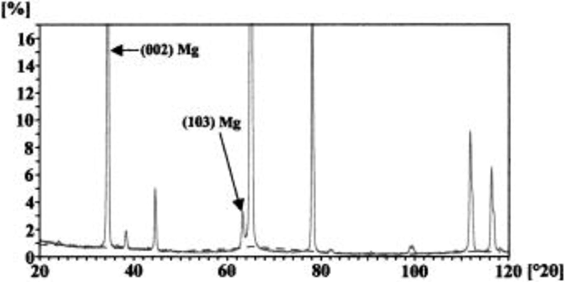
Figure 1. XRD pattern for the Mg-0.4 atom % W alloy before anodizing. The pattern was typical of both sputtering deposited Mg-W alloys. Peaks are present from both the alloy (indicated by arrows) and from the aluminum substrate.
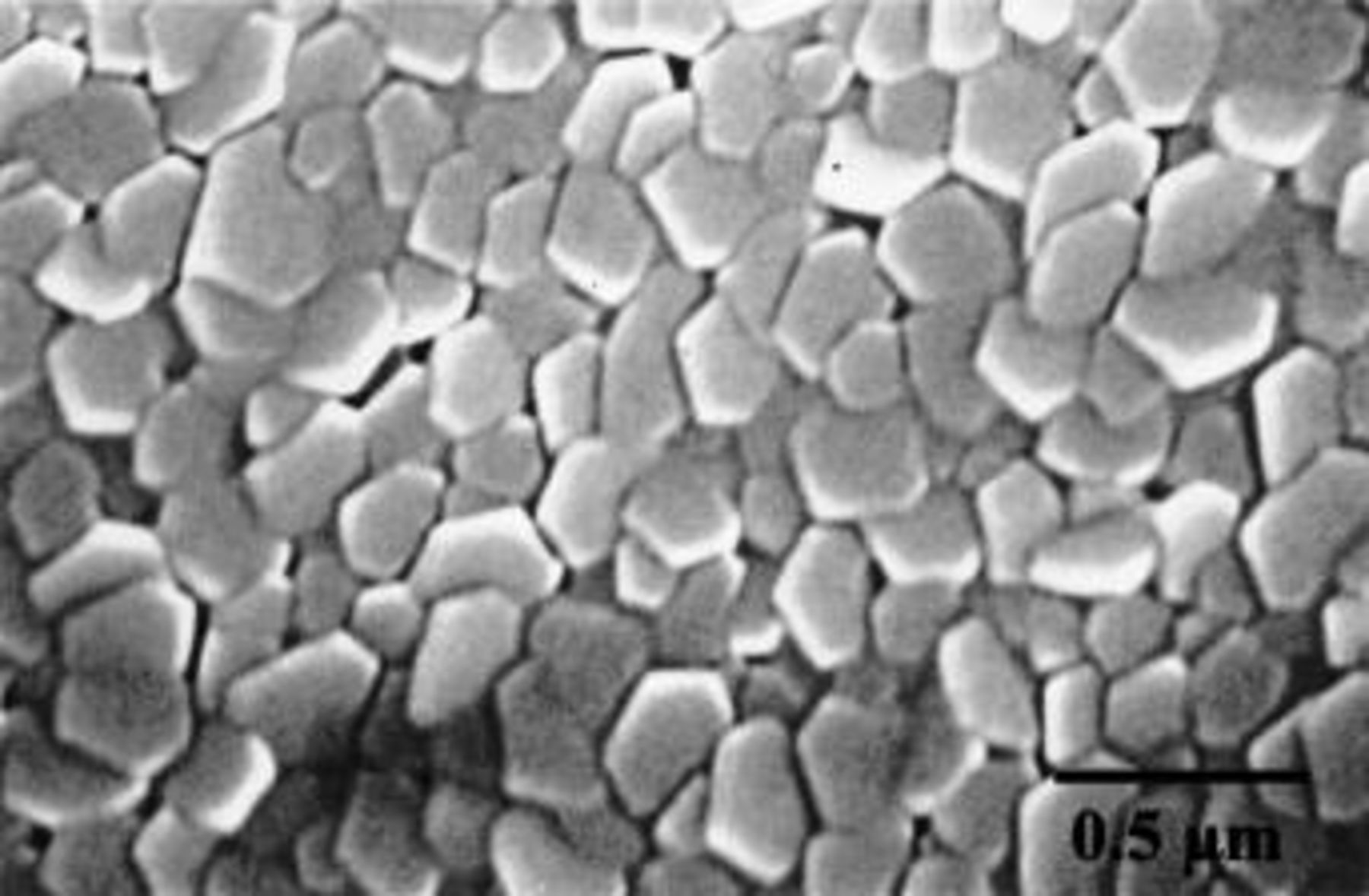
Figure 2. SEM of the surface of the Mg-0.4 atom % W alloy before anodizing.
Voltage-time response.—
The voltage-time responses, which were similar for both alloys, revealed several features that were highly reproducible. The response for the Mg-1 atom % W alloy is shown as a typical example (Fig. 3). The voltage initially rose rapidly, within 1 s, to about 10 V, probably due to the influence of the air-formed film on the alloy. There followed a linear region, with slope  which terminated in the range 40-60 V. After a brief transition region, the voltage again increased linearly to the range 140-170 V, but with the slope reduced to
  Thereafter, the slope decreased gradually until the end of the experiment at 330 V. The drop in voltage toward the end of the anodizing in Fig. 3b is due to oxidation of most of the thickness of the deposited alloy. Sparking was visible above 270 V, associated with oscillations in the voltage. Oxygen evolution was not observed in the period prior to sparking.
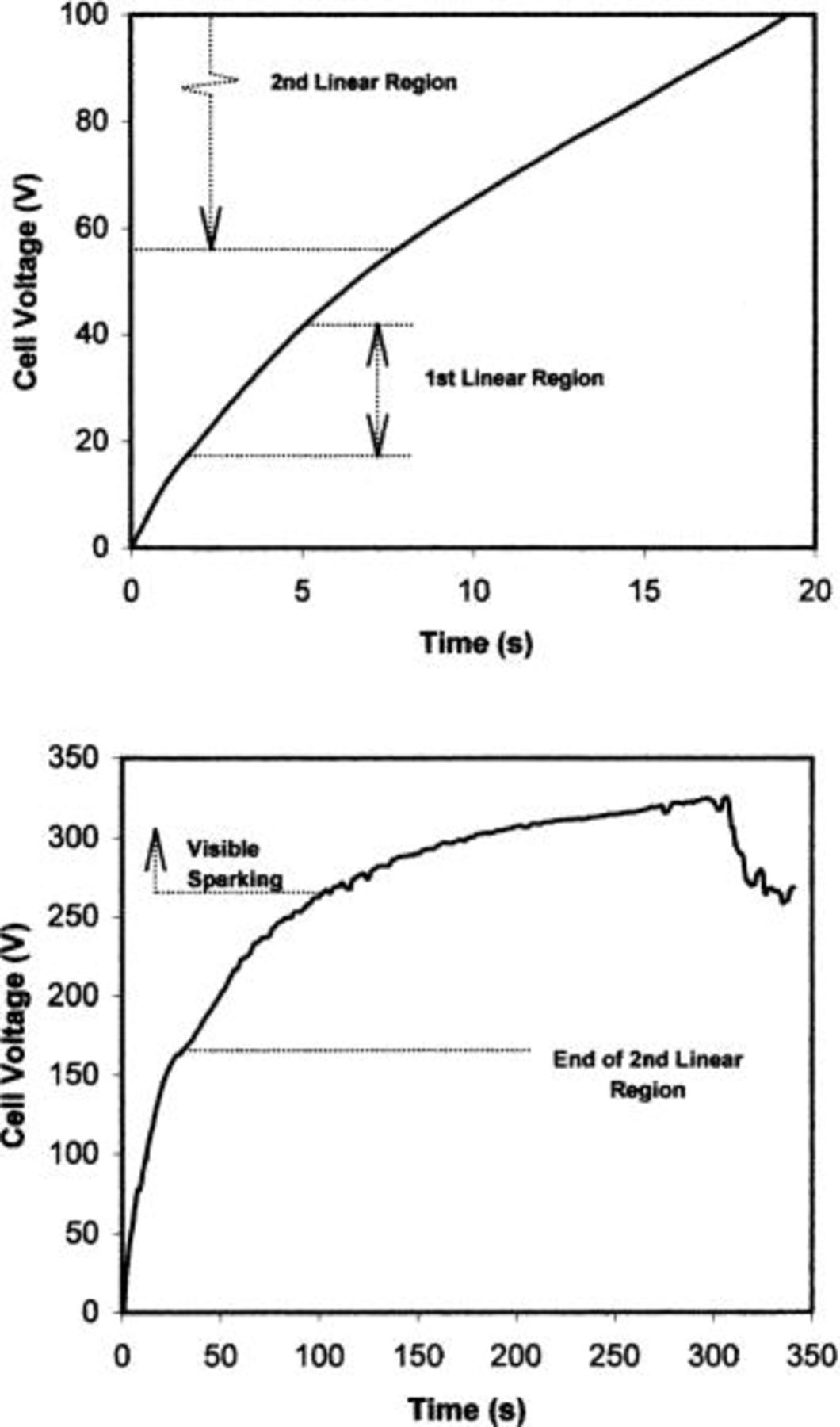
Figure 3. Voltage-time response for the Mg-1.0 atom % W alloy anodized at 10 mA cm−2 in 3 M ammonium hydroxide/0.05 M ammonium phosphate electrolyte at 293 K. (a, top) The response in the voltage range to 150 V, revealing two linear regions. (b, bottom) The response in the voltage range to 330 V. The voltage-time response for the Mg-0.4 atom % W alloy was similar.
The appearance of the alloy was bright and lustrous. The specimens became slightly dull during anodizing to the end of the first linear region and increasingly so during anodizing to the end of the second linear range. In the final, nonlinear region, the specimen became off-white and without luster.
Morphology of anodic films.—
The morphology of the anodic film changed with the progress of anodizing. The general findings were similar for both alloys, and it suffices to describe the results for one alloy. In the first linear period of the voltage-time response, the film was relatively smooth and uniform when examined at low magnification. The grains of the alloy were evident beneath the anodic film (Fig. 4).
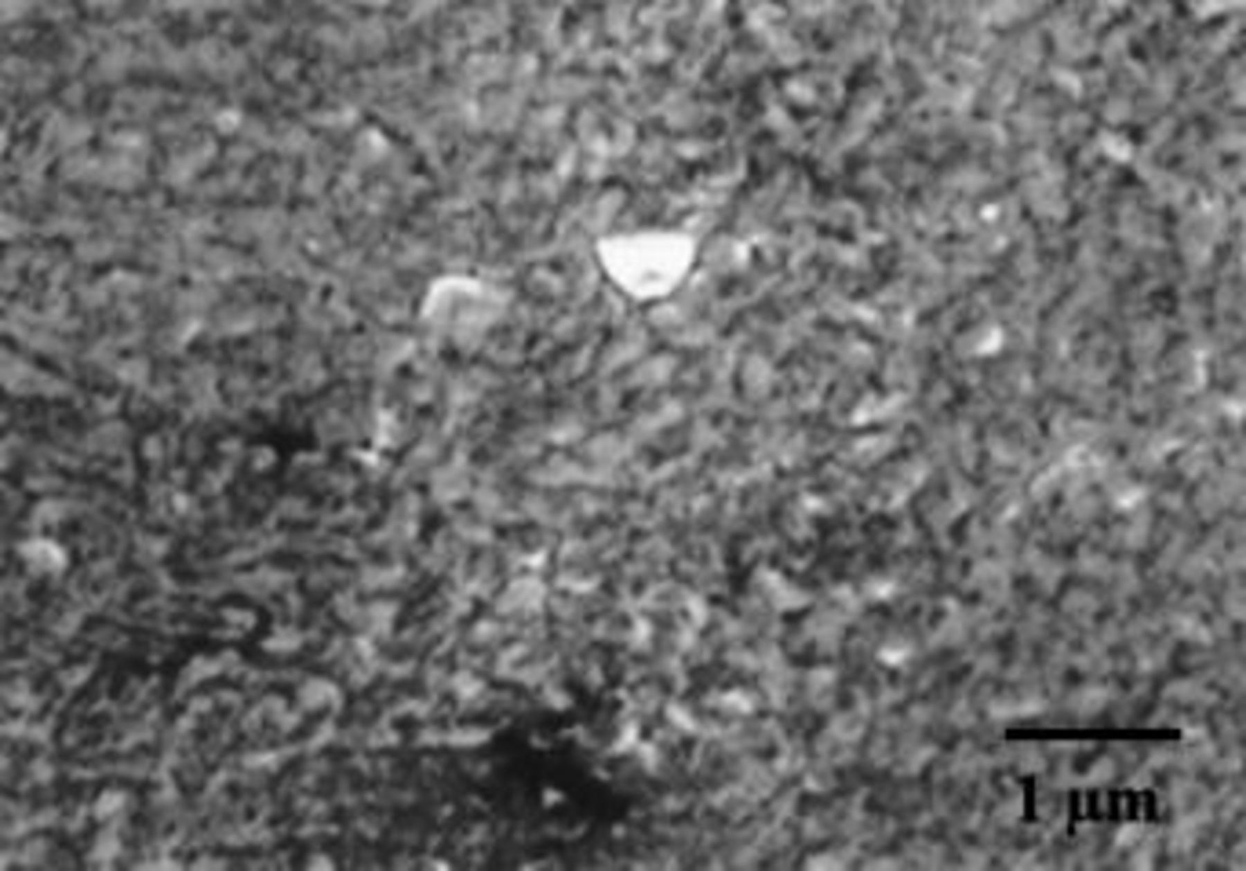
Figure 4. SEM of the surface of Mg-0.4 atom % W alloy following anodizing at 10 mA cm−2 to 50 V in 3 M ammonium hydroxide/0.05 M ammonium phosphate electrolyte at 293 K. Typical appearance of surface, with the influence of the alloy grains evident.
In the second linear region of the voltage-time response, dielectric breakdown developed patches of modified film material, of light appearance in scanning electron micrographs (SEMs; Fig. 5a.) The area of modified film increased as the voltage increased. The modified film revealed pores of typical diameter in the range 25-250 nm, with separations up to about 350 nm (Fig. 5b). Dendrite-like features were common on the surface of the film adjacent to the regions of dielectric breakdown, with their orientation suggesting growth from the breakdown sites (Fig. 5c). Examination at high magnification of the relatively uniform regions remote from the dendrite-like material disclosed variously shaped fine features on the surface of the anodic film. Some approximately circular features suggested pores, with dimensions of the order 10-50 nm and with separation typically in the range 50-100 nm (Fig. 5d). Similar features occurred on the relatively uniform regions at lower voltages. Plate-like material was sometimes present at regions of dielectric breakdown. Such plates, some of roughly hexagonal shape and others more irregular, with typical dimensions in the range 5-20 μm, were variously orientated with respect to the surface of the film and often appeared to be embedded in the film (Fig. 5e). The number of such plates increased with increasing voltage, with populations of about  and
and  at 100 and 150 V, respectively.
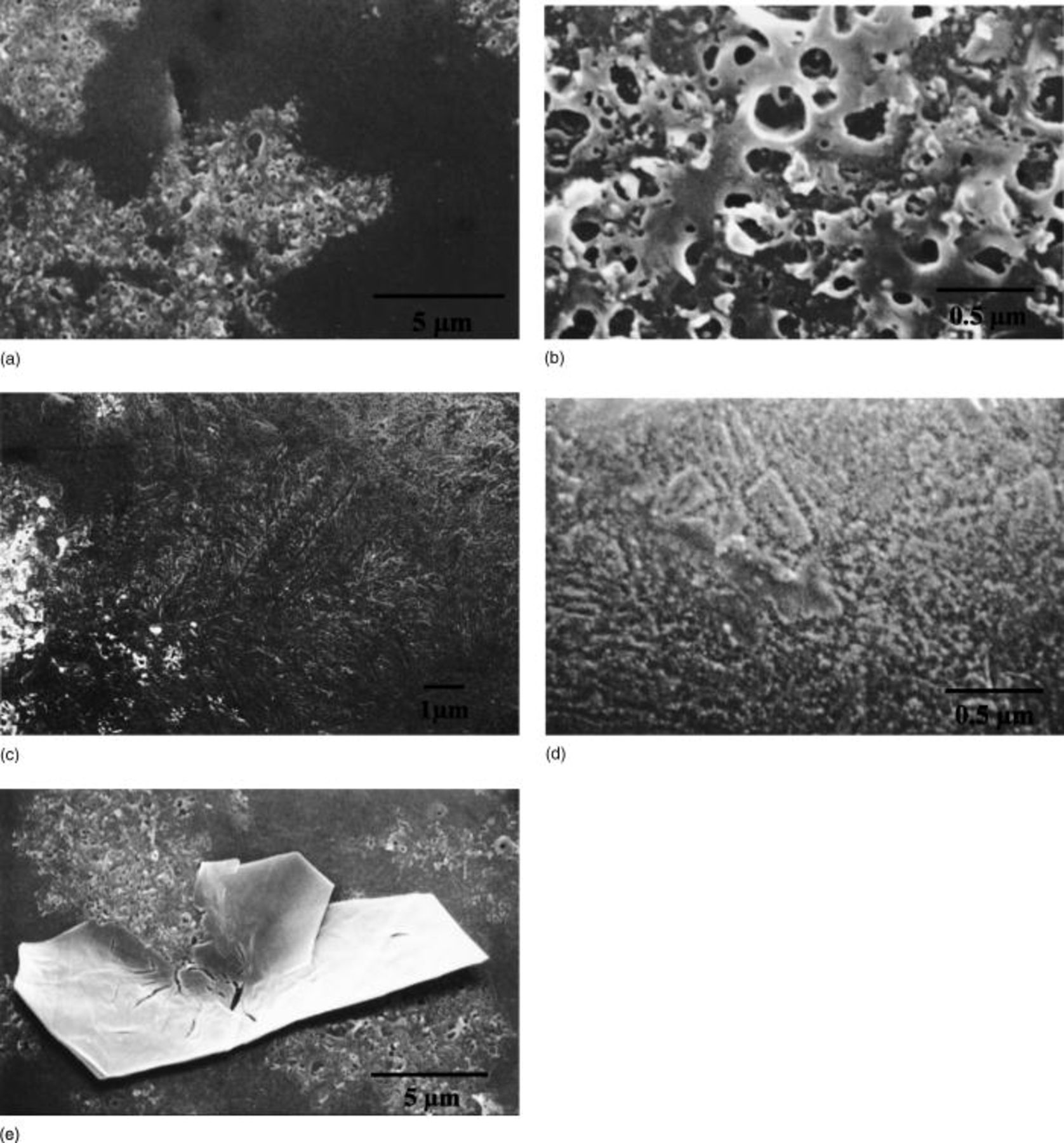
Figure 5. SEMs of the surface of Mg-0.4 atom % W alloy following anodizing at 10 mA cm−2 to 150 V in 3 M ammonium hydroxide/0.05 M ammonium phosphate electrolyte at 293 K. (a, top left) Typical appearance of the surface, with regions of film modified by dielectric breakdown appearing as lighter regions. (b, top right) Detail of a region of dielectric breakdown. (c, center left) A dendrite-like feature on the surface of the film adjacent to a region of dielectric breakdown. (d, center right) Detail of the surface of the unmodified film at a region remote from the dendrite-like features. (e, bottom left) Plate-like material found in regions of dielectric breakdown.
Beyond the linear regions of the voltage-time response, the film morphology was of a uniform porous type, with coarser features than those observed at lower voltages (Fig. 6). The diameter and separation of pores were generally about 0.5-3 μm and 1-10 μm, respectively.
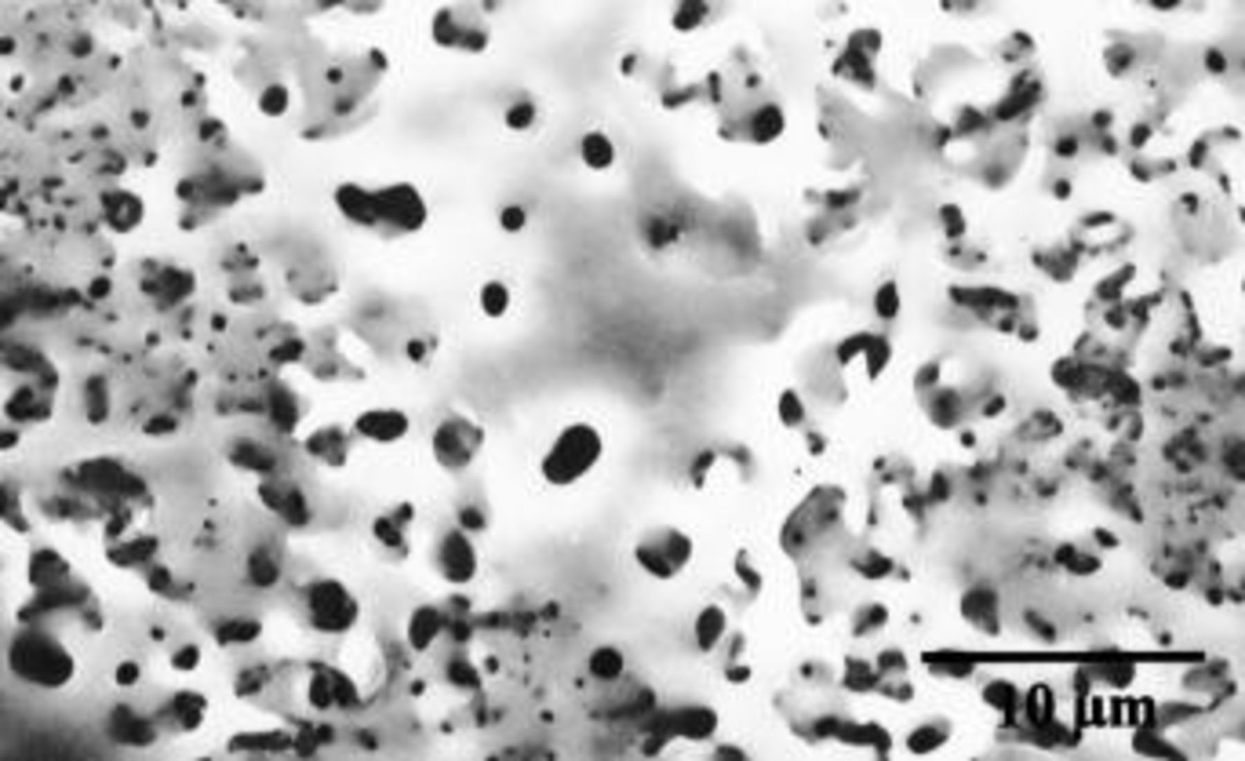
Figure 6. SEM of the surface of Mg-0.4 atom % W alloy following anodizing at 10 mA cm−2 to 330 V in 3 M ammonium hydroxide/0.05 M ammonium phosphate electrolyte at 293 K. The film morphology is uniform across the surface of the specimen, with relatively coarse pores compared with those in the regions of initial dielectric breakdown.
A cross section of a film formed to 100 V on the Mg-0.4 atom % W alloy was prepared by ultramicrotomy for examination by AFM (Fig. 7). The section was cut immediately prior to observation. The layers in the image, in order from the bottom, are the aluminum, the anodic alumina, the Mg-W alloy, the anodic film on the alloy, and the resin used to mount the specimen for sectioning. The anodic film on the aluminum, which was formed at 5 mA cm−2 to 150 V was 180 nm thick, calculated using a formation ratio of 1.2 nm V−1.27 This film provided a calibration of the AFM image. The cross section showed regions of the alloy with film material of relatively uniform thickness, about 180 nm. At other regions, presumed to be associated with breakdown, the film was less uniform, with thickness to about 400 nm. Notably, the film appeared to contain linear pores extending almost through the film, with typical diameters in the range 30-60 nm and separation in the range 50-100 nm.
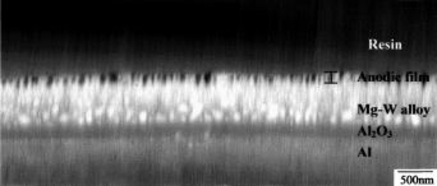
Figure 7. AFM image of a cross section of Mg-0.4 atom % W alloy following anodizing at 10 mA cm−2 to 100 V in 3 M ammonium hydroxide/0.05 M ammonium phosphate electrolyte at 293 K.
Composition of anodic films.—
Qualitative EDX analyses of a film formed to 150 V revealed peaks for magnesium, phosphorus, oxygen, and tungsten (Fig. 8). The penetration of the electron beam to the substrate produced a signal from aluminum. Phosphorus species, which derive from the anions of the electrolyte, were present both at relatively uniform regions and at modified regions. Differences in composition between the two types of regions could not be resolved for films formed up to 150 V. However, the film material formed when sparking was prevalent contained increased amounts of phosphorus species.

Figure 8. Results of EDX analyses in the scanning electron microscope of Mg-0.4 atom % W alloy following anodizing at 10 mA cm−2 to 150 V in 3 M ammonium hydroxide/0.05 M ammonium phosphate electrolyte at 293 K.
The elemental depth profiles of a film formed to 100 V on the Mg-0.4 atom % W, determined by GDOES (Fig. 9), revealed magnesium, phosphorus, and oxygen species, detected previously by EDX analysis, throughout the film. The concentration of phosphorus species appeared to be enhanced near the film surface. Tungsten species, if any were present in the film, were limited to the vicinity of the alloy/film interface. Nitrogen and hydrogen species, which were undetected by EDX analysis, were distributed throughout the film thickness, with a higher concentration of hydrogen toward the surface of the film. Nitrogen, and probably some hydrogen, derives from ammonium ions of the electrolyte. Hydrogen species may also originate from water molecules and hydroxide ions and any hydrogen incorporated into the alloy during sputtering deposition. Although the profiles suggest nonuniform distributions of some species, the signals originate from both regions of relatively smooth film and regions of dielectric breakdown, which may be of differing composition and thickness.

Figure 9. Depth profiles, determined by GDOES, of species in Mg-0.4 atom % W alloy following anodizing at 10 mA cm−2 to 100 V in 3 M ammonium hydroxide/0.05 M ammonium phosphate electrolyte at 293 K. The substrate material, onto which the Mg-W alloy was deposited, was electropolished aluminum.
Results of RBS relating to the enrichment of tungsten in the alloy, that occurs due to the initial formation of an anodic film containing essentially no tungsten species, have been reported previously.28 Here, the focus is on the compositions of the anodic films. The amount of phosphorus species in the films increased with voltage up to 220 V (Fig. 10a and b and 11). The alloy layers anodized to 15 and 100 V were deposited on electropolished and electropolished and anodized aluminum substrates, respectively, which accounts for some differences in the forms of the RBS spectra. The peak in the yield from tungsten in Fig. 10b is due to enrichment of tungsten in the alloy immediately beneath the anodic film.28 The incorporation of phosphorus species increased with the progress of anodizing when expressed in terms of either voltage (Fig. 11a) or charge passed in anodizing (i.e., the product of the current density and the time of anodizing) (Fig. 11b). For films formed to 100 V and above, the results suggested phosphorus species were present throughout the thickness of the anodic film, as found by GDOES. However, it is possible that a few nanometers of phosphorus-free film material, which cannot be resolved by the analyses, may exist adjacent to the alloy/film interface.
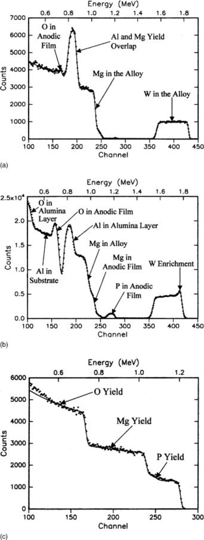
Figure 10. Experimental and simulated (solid line) RBS spectra for Mg-0.4 atom % W alloy following anodizing at 10 mA cm−2 to (a, top) 15, (b, middle) 100, and (c, bottom) 330 V in 3 M ammonium hydroxide/0.05 M ammonium phosphate electrolyte at 293 K.

Figure 11. (a, top) The amount of phosphorus in anodic films formed on Mg-0.4 atom % W and Mg-0.1 atom % W alloys following anodizing at 10 mA cm−2 to various voltages in 3 M ammonium hydroxide/0.05 M ammonium phosphate electrolyte at 293 K. (b, bottom) Expressed with respect to the charge passed in anodizing.
The yield from magnesium disclosed a step, resolved for specimens anodized at voltages above 50 V (Fig. 10b), resulting from the presence of magnesium species in the anodic film. The leading edge of the yield from magnesium was staggered due to the contributions from isotopes of atomic mass 24, 25, and 26 with respective natural abundance of 79, 10, and 11%. The fitting of the step for magnesium and the yield from oxygen indicated on O:Mg atomic ratio of about 2, suggesting a film composed primarily of hydroxide. (Hydrogen cannot be detected by the RBS analyses.) The magnesium content of the films increased progressively with the voltage and charge passed in anodizing (Fig. 12). The P:Mg atomic ratio for films formed to 100 and 150 V was about 0.07. There were no significant signals from nitrogen, indicating the atomic concentration of nitrogen was less than 5% of that of oxygen. In agreement with EDX analyses, the film material formed to 330 V, with sparking, contained increased amounts of phosphorus species (Fig. 10c), with a P:Mg:O atomic ratio of about 1:1.3:3.5. The ratio applies to the outer ∼500 nm of the film thickness that was accessible to the analysis.

Figure 12. (a, top) The dependence upon voltage of the amount of oxygen (from NRA) and magnesium (from RBS) in anodic films formed on Mg-0.4 atom % W and Mg-1.0 atom % W alloys following anodizing at 10 mA cm−2 to various voltages in 3 M ammonium hydroxide/0.05 M ammonium phosphate electrolyte at 293 K. (b, bottom) Expressed with respect to the charge passed in anodizing.
The oxygen contents of specimens both before and after anodizing were determined by NRA. This technique provides a more accurate analysis than RBS, since in RBS spectra the yields from oxygen are relatively low and are superimposed on, and in some cases partly obscured by, the yield from the substrate. A typical spectrum revealed yields from oxygen associated with the anodic films and any oxygen impurity in the alloy, and from carbon contamination that was probably located on the specimen surface (Fig. 13). The oxygen content of the specimens increased progressively with an increase of anodizing voltage, with a steeper rise at higher voltages (Fig. 12a). The data are approximately linearly dependent upon the charge passed during anodizing (Fig. 12b). The amounts of oxygen (from NRA) and magnesium (from RBS) species in films formed to voltages of 100 to 220 V indicated an average O:Mg atomic ratio of 2.1-1.7, decreasing with an increase in voltage. Thus, in agreement with the results of RBS, the films are based on  rather than MgO (Fig. 12b). A part of the oxygen is associated with the phosphorus species, which are probably present in the unmodified film as
  ions. The amount of oxygen associated with the phosphorus species increases with an increase in voltage. Thus, films at higher voltages may be composed of oxyhydroxide.
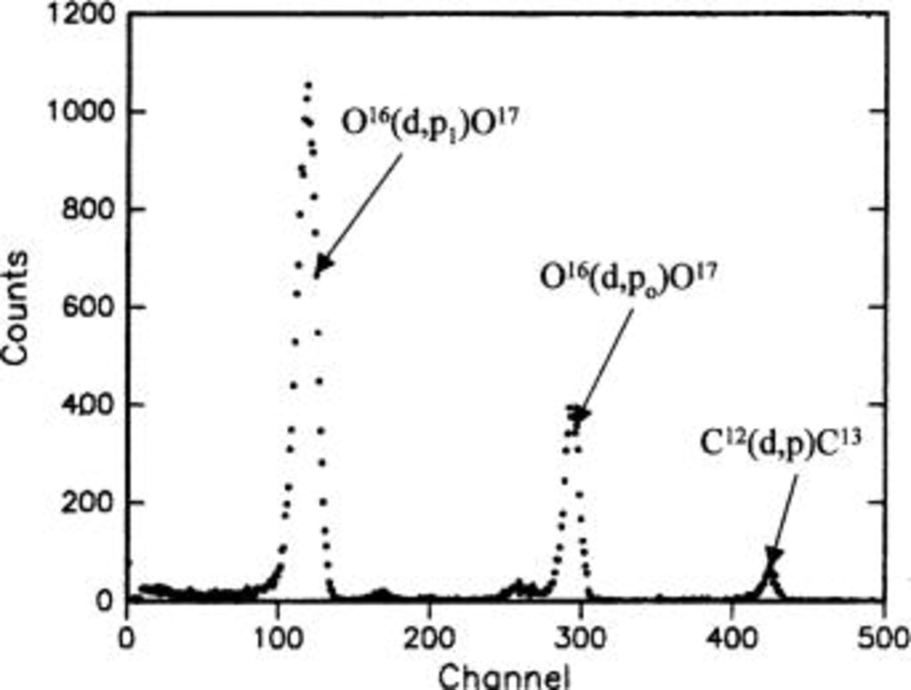
Figure 13. Typical results of NRA, in this case for Mg-0.4 atom % W alloy following anodizing at 10 mA cm−2 to 100 V in 3 M ammonium hydroxide/0.05 M ammonium phosphate electrolyte at 293 K. The three main peaks in order of increasing channel number correspond to the 
 and
and  reactions, respectively. The first of these peaks was used in determination of oxygen contents.
The oxygen content of a typical specimen before anodizing was  oxygen atoms cm−2, measured for an alloy deposited on electropolished aluminum. Following deduction of
  oxygen atoms cm−2 due to the surface film on the electropolished aluminum (assumed to consist of a layer of
  of 2 nm thickness), the upper limit on the oxygen content of the air-formed film on the magnesium alloy was about
  oxygen atoms cm−2. In reality, some of this oxygen may arise from oxygen impurity in the alloy from the sputtering process. Further, the influences of roughness and any porosity have been neglected.
The atomic ratio of phosphorus to oxygen, determined by combining results of RBS and NRA, was about 0.03 in films formed up to 50 V (Fig. 14a). The ratio then increased with further anodizing, to about 0.13 for a film formed to 220 V and about 0.29 (measured by RBS) for the outer region of the film at 330 V. A slower increase of the ratio at higher voltages is evident if the data are presented with respect to the charge passed in anodizing (Fig. 14b).
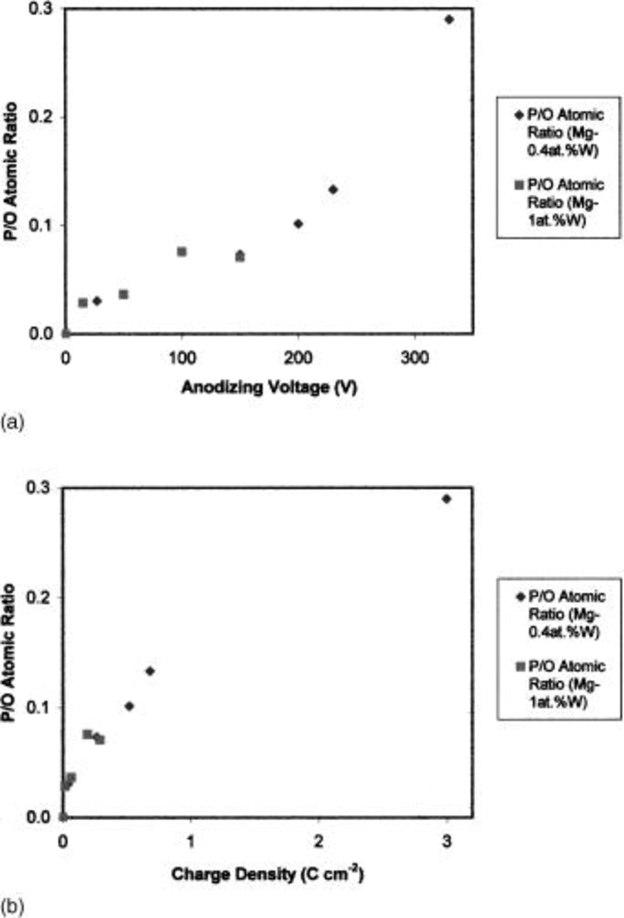
Figure 14. (a, top) Atomic ratio of phosphorus to oxygen for anodic films formed on Mg-0.4 atom % W and Mg-1.0 atom % W alloys following anodizing at 10 mA cm−2 to various voltages in 3 M ammonium hydroxide/0.05 M ammonium phosphate electrolyte at 293 K. (b, bottom) Expressed with respect to the charge passed in anodizing.
Structure of anodic films.—
X-ray diffraction (XRD) patterns of specimens anodized to 220 V revealed only peaks of the alloy and the underlying aluminum substrate, indicating that the anodic film is mainly amorphous or microcrystalline (Fig. 15a). In contrast, the film formed to 330 V, which had experienced sparking, revealed small peaks due to crystalline MgO (periclase) (Fig. 15b). For the latter specimen, peaks were still evident from residual magnesium alloy; about this voltage, most of the alloy layer had been consumed.

Figure 15. XRD pattern for Mg-0.4 atom % W alloy following anodizing at 10 mA cm−2 to (a, top) 150 and (b, bottom) 330 V in 3 M ammonium hydroxide/0.05 M ammonium phosphate electrolyte at 293 K.
Discussion
Development of the anodic film.—
The present results reveal the stages of growth of anodic films on dilute magnesium alloys at a constant current density in the selected alkaline phosphate electrolyte. The main material of the films formed to about 220 V has an O:Mg ratio in the range 2.1-1.7, consistent with magnesium hydroxide or oxyhydroxide. The film also contains phosphorus and possibly nitrogen species. Tungsten species are absent from the film, since tungsten is enriching in the alloy immediately beneath the present anodic films.28 This enrichment of tungsten is due to the preferential oxidation of magnesium in the initial stages of film growth, associated with the lower Gibbs free energy per equivalent for formation of MgO compared with that for  The tungsten cannot be oxidized until its activity is sufficiently increased in the alloy layer immediately beneath the anodic film.
A relatively smooth film, with a finely porous cellular morphology, develops in the period of anodizing to about 50 V as the voltage increases linearly, with a slope of  Around 50 V, dielectric breakdown commences. Thereafter, patches of film material transformed by dielectric breakdown, that produces a coarser porous morphology, spread across the specimen. Thus, the film comprises regions of both cellular and modified film. The changing morphology of the film coincides with a reduction in the slope of the voltage-time response to
  The film material at sites of dielectric breakdown, where the local current density and temperature are high, is of altered composition, especially evident from the enhanced amounts of phosphorus species (Fig. 11). The linear region of reduced slope ends at about 150 V. At higher voltages, the film material transforms further, under the influence of sparking above 270 V, and a relatively uniform porous film eventually covers the specimen.
From the results of NRA, the oxygen in the films increased at  oxygen atoms
  during anodizing of the Mg-0.4 atom % W and Mg-1.0 atom % W alloys to 230 V. The thickness of film material formed can be estimated assuming a film composed of
  The ionic density of the
  is assumed to be 85% that of the crystalline form (brucite,
  ) to account for the amorphous structure of the films. Accordingly, the density of oxygen is
  The thickness of the film formed to 100 V, for which the charge passed was about 0.192 C cm−2, is therefore about 120 nm. This compares with 180 nm for the cross section of the film examined by AFM. The lower calculated thickness can probably be explained by the presence of pores in the film.
Formation of the film.—
The morphology of the film formed initially appears to be similar to that of porous anodic alumina films, which consist of hexagonal cells containing roughly cylindrical pores oriented at approximately 90° to the metal/film interface. The growth of such films occurs at the metal/film interface by migration of  ions inward through the film. Field-assisted ejection of outward migrating
  ions and field-assisted dissolution of film material proceed at the base of the pores. For anodizing at constant current, an initial linear voltage rise, during which a barrier film forms and pores initiate, is followed by a transition to a region of constant voltage when the steady-state morphology of the pores is attained. In the latter stage, the porous region of the film thickens at a constant rate, while a layer of constant thickness is present adjacent to the metal/film interface.
In the case of the present films, a similar mechanism of film growth may occur at the cellular regions, with counter migration of anions and cations through the barrier layer at the base of the porous film. The barrier layer is possibly composed of MgO. Phosphorus species are incorporated into the barrier layer, as considered below. The barrier material subsequently forms the porous region, where the field is low. Hydration of the porous material probably occurs, which is consistent with an apparent abundance of hydroxide species in the films.
The thickness of the barrier layer appears to be relatively small, since the layer could not be resolved by AFM. If it is assumed that the barrier layer represented about one-tenth the thickness of the film formed to 100 V, the layer is about 12-18 nm thick. Presuming that the voltage is dropped across this layer, an electric field of about  is suggested, which agrees with previous estimates of a relatively high field from measurements of barrier layer thickness by TEM.25 For the present films, the thickness of the barrier layer presumably increases with an increase of the anodizing voltage. The pore diameter may also change if behavior is similar to that of aluminum, for which the pore diameter increases with an increase of voltage. Thus, a steady-state pore morphology may not be achieved.
Incorporation of phosphorus species into the film.—
The growth of the initial cellular film proceeds with incorporation of phosphorus species into the film material. Incorporation of species derived from electrolyte anions is common in the growth of anodic films. It has been studied in detail for barrier films formed on aluminum and tantalum in phosphate electrolytes.35 36 The phosphorus species occupy an outer layer of the film, with a layer of either pure alumina or pure tantala separating the phosphorus-containing region from the metal. The layering of the film composition is due to phosphate ions migrating more slowly than oxygen ions in the film.37 There are no short-circuit pathways for phosphorus species to reach the metal/film interface. Similar phosphorus incorporation proceeds for porous anodic films on aluminum, with phosphorus being present in the porous regions and also in the barrier region but with a layer of phosphorus-free alumina being present adjacent to the metal/film interface. Phosphorus species in the films formed on the Mg-W alloys appear to extend to the alloy/film interface, although it is possible that there may be a thin, unresolved layer of phosphorus-free material remaining next to the metal. The level of phosphorus incorporation, with a P:O ratio of about 0.03 is similar to that found for the phosphorus-containing region of barrier-type alumina films, which were in the approximate range 0.01-0.03 depending upon forming conditions.35
The amount of phosphorus species in the film relative to oxygen and magnesium in the film rises rapidly with the onset of dielectric breakdown. At the highest voltage investigated, namely, 330 V, the P:O atomic ratio is about 1:3.5, compared with about 1:33 for the barrier-like film. Thus, the processes occurring at breakdown form material of significantly modified composition. Further work is necessary to examine the nature of phosphorus species in the films. It is likely that phosphate ions are present in the barrier-like film. Some rise in phosphate incorporation may occur at breakdown sites due to the formation of film material at increased current density and temperature. However, the phosphate ions of the electrolyte may be transformed to other species under the extreme conditions of breakdown, particularly with the onset of sparking. The P:Mg:O ratio for the surface region of the film formed to 330 V was about 1:1.3:3.5, which also indicates an enhanced oxygen content compared with films formed at 220 V and below, for which the O:Mg ratio was roughly 2. The formation of film material under sparking conditions is not understood clearly. Extreme temperatures, possibly of several thousand degrees kelvin, leading to molten material may be involved. The possible operative processes have been reviewed recently.38
Efficiency of film growth.—
The reduction in slope of the voltage-time response on passing from the initial to the second stage of anodizing indicates a decrease in the efficiency of film growth. The decrease in efficiency is associated with the start of dielectric breakdown and the consequent formation of film material modified by dielectric breakdown. It is probable that magnesium species are lost to the electrolyte at sites of breakdown. At the adjacent regions, the film thickens with increase in voltage. However, such film is eventually replaced and the voltage increases more slowly as current is consumed largely by breakdown processes.
The efficiency of formation of film was estimated from the charge associated with oxygen in the film. The amount of oxygen in the specimens is known from NRA and is assumed to be present as  ions. The oxygen present before anodizing, probably due mainly to air-formed oxide/hydroxide, was deducted so that only that added during anodizing was considered. The charge associated with the oxygen species of the film material, compared with that passed in anodizing, indicates an efficiency of about 60-65% for formation of the initial film, which declines to typically 40-50% for voltages from 50 to 220 V (Fig. 16). The oxygen species are assigned a charge of unity, i.e., corresponding to
  ions. The calculation neglects that some of the oxygen is probably present as
  ions, and as such contributes relatively less to the charge passed in anodizing. A correction can be made assuming that the
  ions are incorporated into the film as units of
  and hence that one of these oxygen atoms is associated with the charge passed in forming 3/8 magnesium ions. For the mainly uniform initial film, the correction is minor due to the relatively low phosphorus content. The required correction is more uncertain for films modified by dielectric breakdown, since the nature of the phosphorus species is unknown. Any contributions from side reactions, such as oxygen generation, would lead to further reductions in efficiency. In contrast, any contributions from
  ions associated with MgO would lead to an increase in the calculated efficiency.

Figure 16. Efficiency of film growth determined from analyses of oxygen and magnesium contents of anodic films formed on Mg-0.4 atom % W and Mg-1.0 atom % W alloys following anodizing at 10 mA cm−2 to various voltages in 3 M ammonium hydroxide/0.05 M ammonium phosphate electrolyte at 293 K (a, above). (b, bottom) Expressed with respect to the charge passed in anodizing.
Alternatively, the charge associated with the film can be estimated from the number of magnesium ions in the film, determined from RBS. The number of magnesium ions in the film, assumed to be present as  ions, can be determined reasonably accurately for these thicker films. The efficiencies agree well with those estimated previously from the oxygen contents of the films (Fig. 16). Any contributions from singly charged magnesium ions would result in a reduction in the calculated efficiency.
The reduced efficiency of formation of barrier-like film indicates loss of magnesium species to the electrolyte by field-assisted ejection of ions from the film, field-assisted dissolution of the film, or chemical dissolution of the film. The dissolved magnesium species appear to form precipitates, with dendrite-like appearances, on the surface of the film, for instance composed of  or
or  The precipitated material may be incorporated into the growing film by overgrowth of film material and or by fresh precipitation. Dendrite-like features are also prevalent near regions of dielectric breakdown, suggesting release of magnesium ions to the solution at breakdown sites and subsequent precipitation. The nature of the platelets that occurred in the vicinity of breakdown sites has not been ascertained. They may represent precipitates or pieces of film that have detached from the substrate.
Incorporation of nitrogen species.—
The presence of nitrogen species throughout the thickness of the film was determined from GDOES analysis of a film formed to 100 V. Since the analysis area extended over regions of cellular film and regions of film modified by dielectric breakdown, it is not possible to separate the incorporation of these species in the two regions of film. The nitrogen content of the films appears to be relatively low, and it is possible that they are adsorbed species on pore walls or incorporated into hydrated material. However, without separate analyses of the film regions, no significant comment can be made on the mechanism of incorporation. Future work will examine thinner films, consisting of barrier-like film alone, with compositional analyses by GDOES and morphological examination by TEM.
Conclusions
1. Anodizing of Mg-0.4 atom % W and Mg-1.0 atom % W alloys at 10 mA cm−2 in 3 M ammonium hydroxide/0.05 M ammonium phosphate-based electrolyte at 293 K results in the following sequence of film development. First, a finely porous film forms during anodizing to about 50 V, with the voltage increasing linearly with time. Second, dielectric breakdown locally modifies the film, forming patches of coarser porous material that gradually spread across the surface of the specimen. At the regions unaffected by breakdown, the film continues to thicken. This stage of film growth manifests a linear increase of voltage with time, to about 150 V, but with a reduced rate. Third, the film transforms to a uniform porous morphology, of increased pore size, with the rate of voltage increase gradually decreasing with time. Sparking and oxygen evolution accompany dielectric breakdown above about 270 V.
2. The anodic films are mainly amorphous or microcrystalline and contain magnesium, oxygen, phosphorus, hydrogen, and possibly nitrogen species. The oxygen to magnesium atomic ratio is in the range 1.7-2.1 during anodizing to 220 V, indicating films based on magnesium hydroxide or oxyhydroxide. The film species are distributed throughout the thickness of the anodic film at the resolution of the experiments. Tungsten enriches in the alloy and accordingly the films are initially free of tungsten species.
3. The films have an atomic ratio of phosphorus to oxygen that increases from about 0.03 for films formed below 50 V, to 0.13 at 220 V and 0.29 at 330 V suggesting compositional modification of the film by dielectric breakdown. Some crystalline MgO is found in the film at 330 V.
4. The anodic films form at a reduced efficiency due to loss of magnesium species to the electrolyte. The efficiency is typically about 40-50% in the range to 220 V. Dendrite-like features on the surface of the anodic film suggest precipitation of magnesium compounds.
5. With onset of sparking, the films develop a porous morphology, with a coarser texture than the porous regions found at lower voltages.
Acknowledgments
The authors are grateful to the Engineering and Physical Sciences Research Council (U.K.) for financial assistance and to Dr. C. Ortega, Groupe de Physiques des Solides, for provision of time on the Van de Graaff accelerator of the Université de Paris VI et VII [work partially supported by Centre National de la Recherche Scientifique (GDR86)].