
Abstract

 samples for
  were prepared by magnetron sputtering using a combinatorial materials science approach. The room-temperature resistivity and X-ray diffraction (XRD) patterns of the samples were used to select materials having both an amorphous structure and good conductivity for further study. The reaction of lithium with amorphous
 was then studied by electrochemical methods and by in situ XRD. The electrode material apparently remains amorphous throughout all portions of the charge and discharge profile, in the range
  in
in 

 No crystalline phases are formed, unlike the situation when lithium reacts with tin. Using the Debye scattering formalism, we show that the XRD patterns of the a-
 starting material and
  can be explained by the same local atomic arrangements as found in crystalline Si and
  Si or
Si or  Sn, respectively. In fact, the in situ XRD patterns of a-
 for any x, can be well approximated by a linear combination of the patterns for
  and
and  This suggests that predominantly only two local environments for Si and Sn are found at any value of x in

 However, based on differential capacity vs. potential results for Li/a-
 there is no evidence for two-phase regions during the charge and discharge profile. Thus, the two local environments must appear at random throughout the particles. We speculate that the charge-discharge hysteresis in the voltage-capacity profile of
  cells is caused by the energy dissipated during the changes in the local atomic environment around the host atoms. © 2002 The Electrochemical Society. All rights reserved.
Export citation and abstract BibTeX RIS
The capacity advantages of lithium alloys compared to graphite are potentially enormous. For example, graphite can store 372 mAh/g corresponding to  and silicon can store 4200 mAh/g corresponding to
  . However, obtaining hundreds of charge-discharge cycles with alloy negative electrodes has proven to be difficult, except when the capacity is constrained to values near that of graphite.1 The reason for failure is believed to be inhomogeneous volume expansion in coexisting regions of phases with different lithium concentrations within the same particle, resulting in particle pulverization.2
In a recent patent application, Turner et al.3 described the utility of amorphous metals and metalloids as negative electrode materials for lithium-ion cells. The advantage of amorphous materials is claimed to be the elimination of two-phase regions between phases of different lithium concentration leading to homogeneous volume expansions4 and improved charge-discharge cycling behavior.
In this paper, we discuss some aspects of a- alloy negatives, which are discussed in the patent application. First, we describe the production of the amorphous alloys by sputtering and the composition range of the amorphous phase. The electrical resistivity of the samples is dramatically reduced as the tin concentration is increased, and therefore we selected a composition, a-
 near the end of the amorphous range for detailed electrochemical and in situ XRD studies.
Experimental
Two sputtering systems and approaches were used to prepare the samples in this work. One sputtering system used is well adapted to making a range of stoichiometries in a single deposition as in combinatorial materials science. The other larger system is well suited to the production of larger quantities of material of a single composition.
Combinatorial magnetron sputtering was performed using a Corona Vacuum Coater's (Vancouver, BC, Canada) V3T system. The system is turbopumped and reaches a base pressure of  Torr. 2 in. diam targets of Si and Sn were used. The sputtering chamber is equipped with a 40 cm diam water-cooled rotating substrate table and a stationary mask platform. The mask openings, shown in Fig. 1, were placed as near to the substrate table as possible. The curved mask opening opposite to the Si target was designed so that a constant Si deposition rate (measured in Å/
 /s) is maintained as a function of r, as shown in Fig. 1 when the substrate table is rotating. The curved mask opening opposite to the Sn target was designed so that a linearly varying deposition rate is achieved as a function of r when the substrate table is rotating. Sputtering and rotation rates were selected so that about one atomic layer of atoms was deposited during each pass under the targets. Both Sn and Si were sputter deposited using dc power supplies, operating at 50 and 300 W, respectively. The Ar flow rate was about 19 sccm, and chamber pressure was maintained at 3.2 mTorr during the deposition. The substrate table angular speed was 20 rpm.
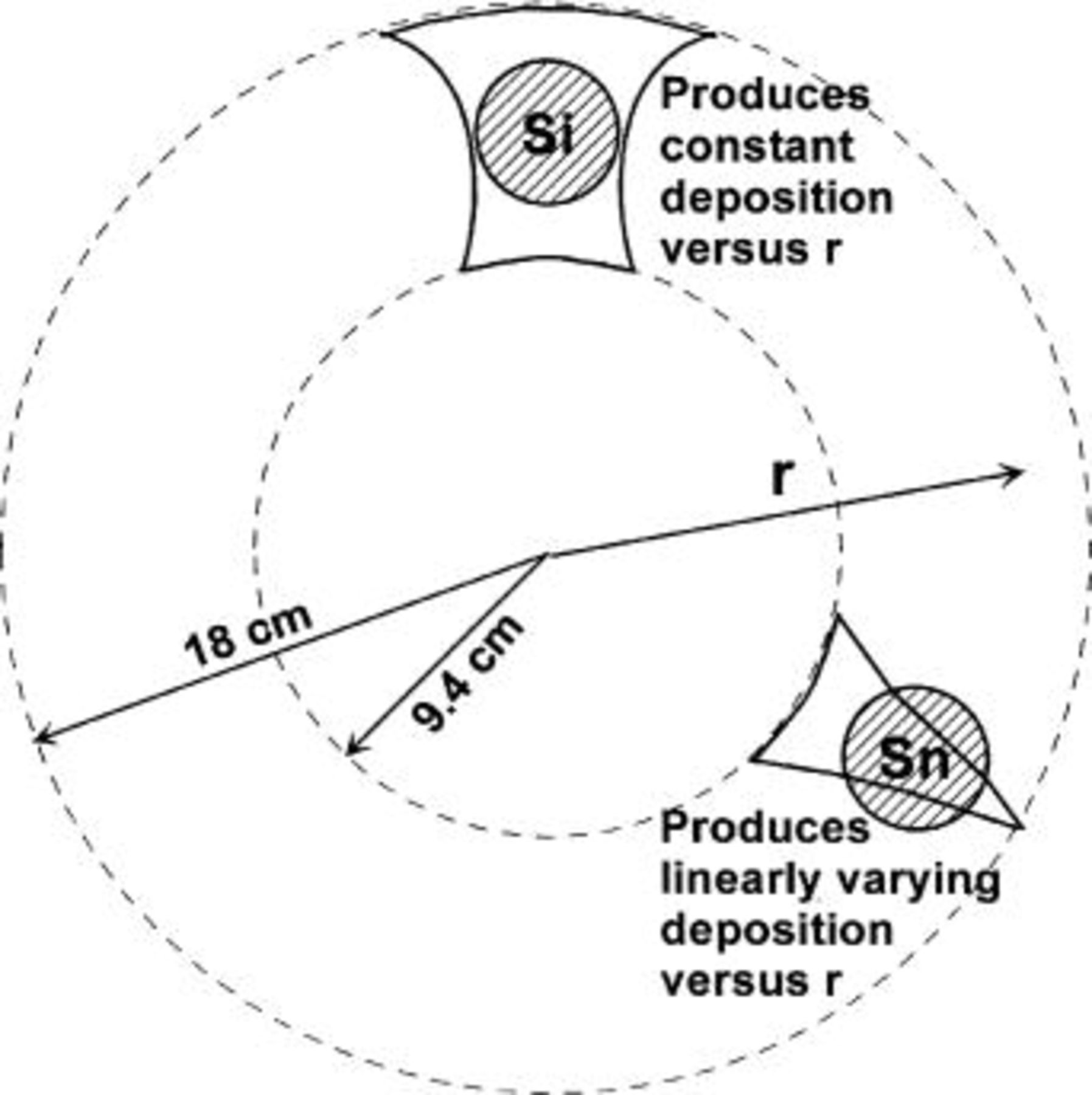
Figure 1. Schematic representation of the setup used inside our sputtering chamber. Sputtering masks are used to deposit a linear range in composition x in a binary system such as 
Sputtering was made on copper foil for battery electrodes, X-ray diffraction (XRD), and compositional analysis, on aluminum foil for mass loading and thickness determinations, and on glass slides for resistivity measurements, all during the same deposition run. The foils and slides were bonded to the water-cooled substrate table using 3M brand Y9415 double-sided adhesive tape. Small rectangular glass slides  mm thick) were placed with their long direction perpendicular to the vector r in Fig. 1 and their distance from the center of the table carefully measured and recorded. The copper foil and glass slides were cleaned first with methanol and then by plasma etching in the sputtering chamber. Masses of the deposited films were determined by weighing 1.3 cm diam Al foil disks before and after sputtering with a Cahn microbalance (±10 μg). Film thickness was estimated from the mass per unit area and the expected density of the deposit, calculated as
Resistivity measurements were made using a two-wire technique with silver-painted contacts to the  films. A two-wire measurement was deemed sufficient because the film resistance was normally between 10 Ω and 10 MΩ.
Composition as a function of r was determined using a fully automated 733 JEOL electron microprobe X-ray microanalyzer equipped with an Oxford Link eXL 131 eV energy-dispersive detector. The 2 μm electron beam was operated at 15 kV and 15 nA.
A large-scale sputtered sample of  was produced using a Perkin Elmer Randex model 2400-8SA sputtering system. Sputtering was made on copper foil that was bonded to a rotating water-cooled substrate table with two-sided tape as described previously. The copper foil was plasma cleaned with moderate energy argon ions (100-150 eV) before deposition for 30 min. A single target (cast at 3M) of composition
  was sputtered using a dc power supply using an argon pressure of 30 mTorr. After sputtering, the film was scraped off the substrate and ground into fine powder (particle size
  μm).
μm).
Electrochemical tests performed in standard two-electrode coin cells.—
Composite electrodes made from 80 wt %  10 wt % Super-S carbon black, and 10 wt % polyvinylidene fluoride (PVdF) were coated on a thin copper foil and tested in 2325 coin cell hardware. Also used in the construction of these cells was a polypropylene microporous separator, electrolyte (1 M
  dissolved in ethylene carbonate/diethyl carbonate 30:70 vol, Mitsubishi Chemical), and lithium metal (FMC Chemicals) as both the reference and counter electrode. All cells were assembled in an argon-filled glove box and tested using constant charge and discharge currents at a constant temperature of
  C.
C.
XRD experiments were conducted on a Siemens D5000 diffractometer using a theta/theta goniometer with a Cu target source. Samples were X-rayed in powder form in a standard well-type sample holder.
In situ XRD was used to study the reaction mechanism during the first two discharge/charge cycles. A composite electrode as described above was deposited on a Be window and assembled in coin-type cells as described in Ref. 5. All in situ experiments were conducted at room temperature with the Siemens D5000 diffractometer described.
In order to interpret the XRD patterns from the amorphous samples, the Debye scattering formalism was used.6 The Debye scattering equation is given by
where  is the scattered intensity in electron units,
  is the scattering power of atom m,
  is the distance between atoms m and n, and
  The Debye scattering formalism sums the scattered amplitude from each atom assembled in a given geometry to simulate XRD patterns.
Results and Discussion
Figure 1 shows a schematic representation of the setup used in our sputtering chamber. The masks placed over the Si and the Sn targets are designed to give a composition x in  such that x varies linearly along the direction radial to the substrate table. Figure 2 shows the measured stoichiometry as a function of the radial distance. The tin composition, x, is near 0.5 at the inner edge of the deposit (begins at 9.4 cm radius) and decreases almost linearly to
  at
at  cm.
cm.
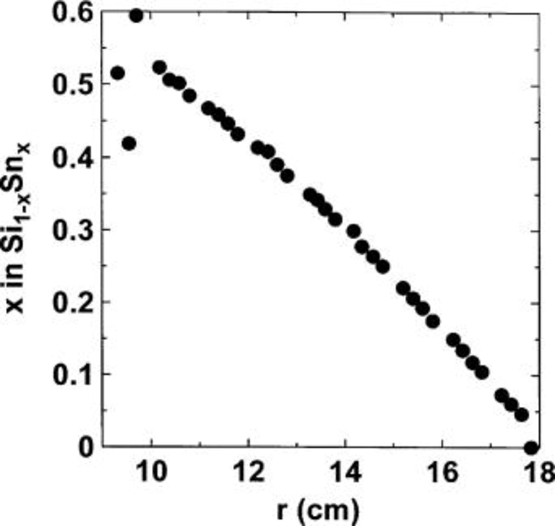
Figure 2. Value of Sn composition x in  plotted as a function of the radial distance from the center of the sputtering table.
Figure 3 shows the resistivity (taken at 21°C) of  vs. x for the films deposited on the rectangular slides. The value of x was determined from the position of the slide (its value of r) and Fig. 2. The resistivity drops dramatically with x, until about
  where a change in slope is observed. The data match that collected by Maruyama and Akagi7 quite well. However, the precision of our data is much higher so that the change in slope at about
  can be observed.
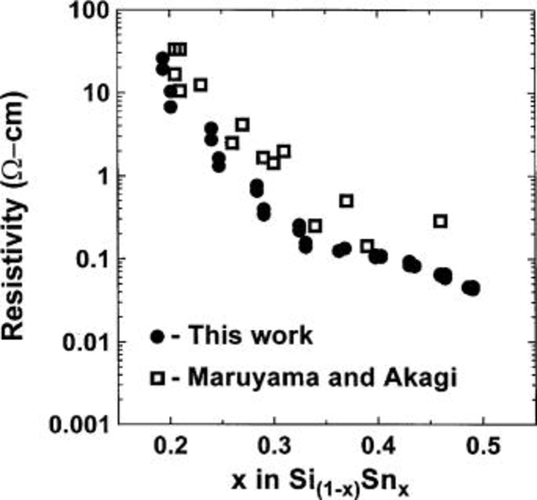
Figure 3. Resistivity (Ω cm) as a function of Sn composition x. (•) data taken by the present authors and (□) data from Maruyama and Akagi.6
Figure 4 shows XRD patterns for representative  samples with
  0.36, 0.40, and 0.53. All samples with
  are amorphous and all samples with
  show evidence for crystalline tin precipitates. We believe that the change in slope of the resistivity graph is probably caused by the onset of tin crystallization. The diffraction patterns of the amorphous samples with
  and 0.36 in Fig. 4 are dominated by the signal from the underlying glass slide because the films are only about 1 μm thick. A better diffraction pattern of a thick powder specimen of amorphous
  is shown later.
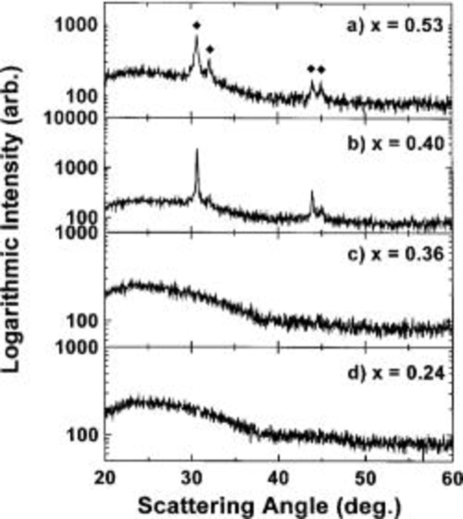
Figure 4. XRD patterns of  for
for  (a) 0.53, (b) 0.40, (c) 0.36, and (d) 0.24.
Based on the results in Fig. 3 and 4, we selected the composition  for electrochemical study.
  has a relatively low resistivity and shows no evidence for the precipitation of crystalline tin.
Figure 5a shows the XRD pattern of powdered  material prepared in the Randex sputtering system. The XRD pattern shows the alloy is amorphous as expected based on Fig. 4. In order to try to understand the structure of this amorphous material, the Debye scattering formalism was used to calculate the diffraction pattern of a single Si unit cube containing 18 atoms, eight on the corners [(0,0,0), (1,0,0), (0,1,0), (0,0,1), (1,1,0), (0,1,1), (1,0,1) and (1,1,1)], six on the faces [(1/2,1/2,0), (0,1/2,1/2), (1/2,0,1/2), (1/2, 1/2,1), (1,1/2,1/2), (1/2,1,1/2)], and four within the cube at (1/4,1/4, 1/4), (3/4,3/4,1/4), (1/4,3/4,3/4), and (3/4,1/4,3/4).6 The calculated result that best matched the
  pattern was obtained when a cube edge of 5.6 Å was used. This is slightly larger than the accepted value
  Å for crystalline Si.6 The increase is probably a result of the larger Sn atoms incorporated substitutionally into a-Si. Although not rigorous, this Debye calculation suggests that
  has a short-range ordered diamond structure, similar to amorphous Si.
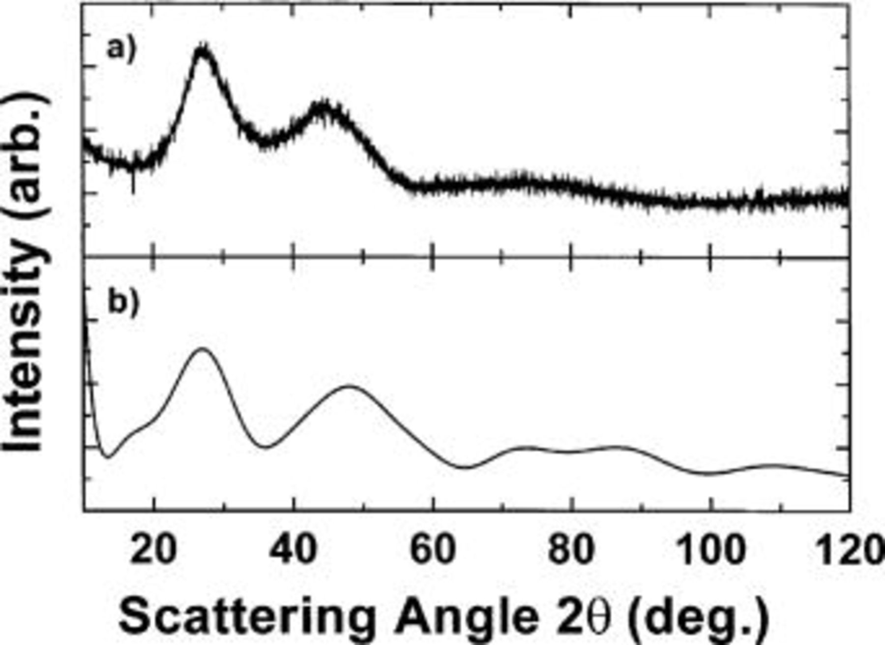
Figure 5. (a) XRD pattern of amorphous  (b) Simulated XRD pattern of a single Si unit cell (with
  Å) using the Debye scattering equation.
Figure 6 shows the voltage vs. capacity (6a) and the differential capacity vs. voltage (6b) of a Li/ cell charged and discharged at 45.5 mA/g (C/42 or 0.04 mA/
 between 1.3 and 0 V vs. pure lithium metal for the first few cycles. The voltage vs. capacity is smooth and continuous, showing the absence of any plateaus indicative of phase changes during the reaction with Li. Plateaus in voltage vs. capacity graphs indicating phase changes appear as sharp peaks in differential capacity vs. voltage. The differential capacity shown in Fig. 6b is smooth and free from sharp peaks.
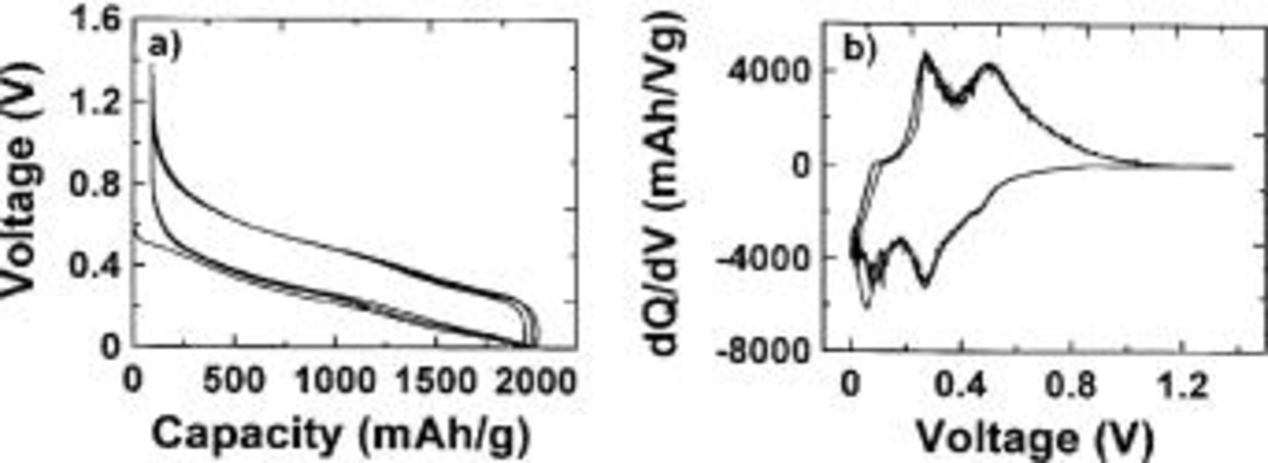
Figure 6. (a) Voltage vs. capacity of a  electrode cycled against Li metal between 0 and 1.3 V. (b) Differential capacity vs. voltage of the cell shown in part a.
Figure 7 shows the in situ XRD results collected during the first discharge cycle of a Li/ cell. The cell was discharged at 19.7 mA/g (C/96 or 0.15 mA/
 to 0.2 V for the first cycle. The voltage vs. capacity curve for the cell collected during the experiment is shown in Fig. 7e. The maximum capacity of 860 mAh/g obtained for the first discharge represents approximately 2 Li atoms per
  formula unit. Some of the XRD patterns collected during the first discharge cycle are shown in order from top to bottom in Fig. 7a-d. The sharp peaks in the diffraction pattern are due to various cell parts. The solid dots on the voltage curve (Fig. 7e) show the starting position at which each X-ray scan shown in Fig. 7a-d was collected. Figure 7a-d shows that the XRD pattern of the electrode develops broad peaks at
  and
and  during the insertion of lithium. The change in the 23° peak can more clearly be seen in Fig. 8a, where the XRD pattern at the bottom of discharge (dark line) is compared to the XRD pattern of the fresh cell. Displaying the two curves together shows the existence of the broad peaks. The broad peaks observed in this work have often been observed in other Li-Sn-containing intermetallics and have been explained in Ref. 8 by the local structure found in
  (or isostructural
  . In this structure, Sn atoms are arranged locally on the corners of tetrahedra that have edges 3.3 Å long.
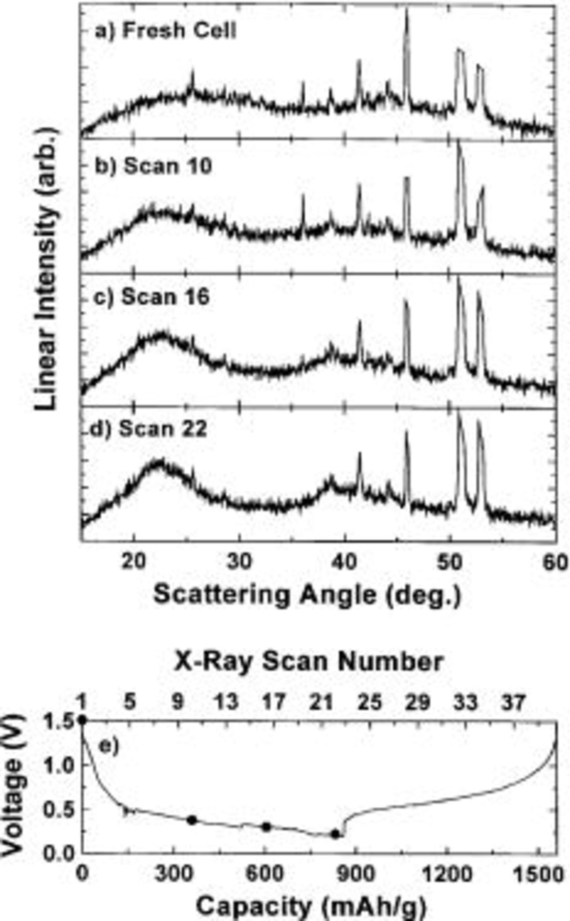
Figure 7. (a-d) In situ XRD patterns collected during the first discharge cycle of a  electrode cycled against Li metal to 0.2 V. The sharp peaks in the diffraction patterns come from various cell parts. (e) Voltage vs. capacity (bottom abscissa) and X-ray scan number (top abscissa) collected during the experiment. (•) indicates where the X-ray scans began.
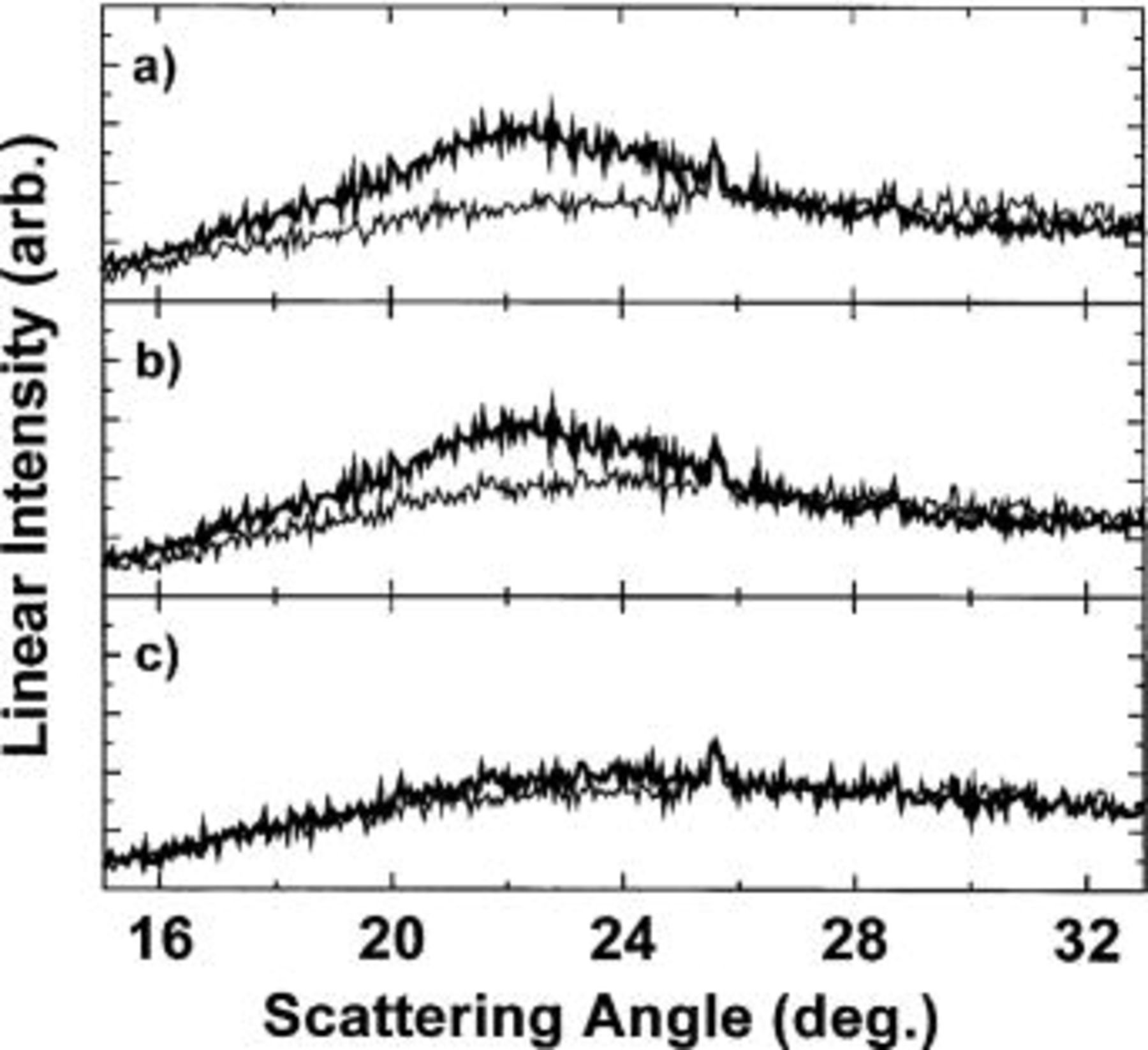
Figure 8. (a) Comparison between the XRD pattern of the (light line) fresh cell and the (dark line) fully discharged cell. (b) Comparison between the XRD pattern of the (dark line) fully discharged cell and (light line) the fully charged cell. (c) Comparison between the XRD pattern of (light line) the fresh cell and (dark line) the fully charged cell.
The results from the first charge of the same Li/ cell are shown in Fig. 9. As lithium is removed from the electrode, the broad peaks (Fig. 9a-d) slowly disappear until the XRD pattern of the electrode at the top of the first charge cycle resembles the XRD pattern of the fresh cell. Figure 8b shows the XRD pattern of the electrode at the bottom of the first discharge cycle (dark line) and the top of the first charge cycle (light line). More importantly, Fig. 8c shows a comparison between the XRD pattern of the fresh cell (light line) and the XRD pattern of the electrode at the top of the first charge cycle (dark line). Little difference is observed between the patterns in Fig. 8c showing that the electrode returns to approximately the starting state.
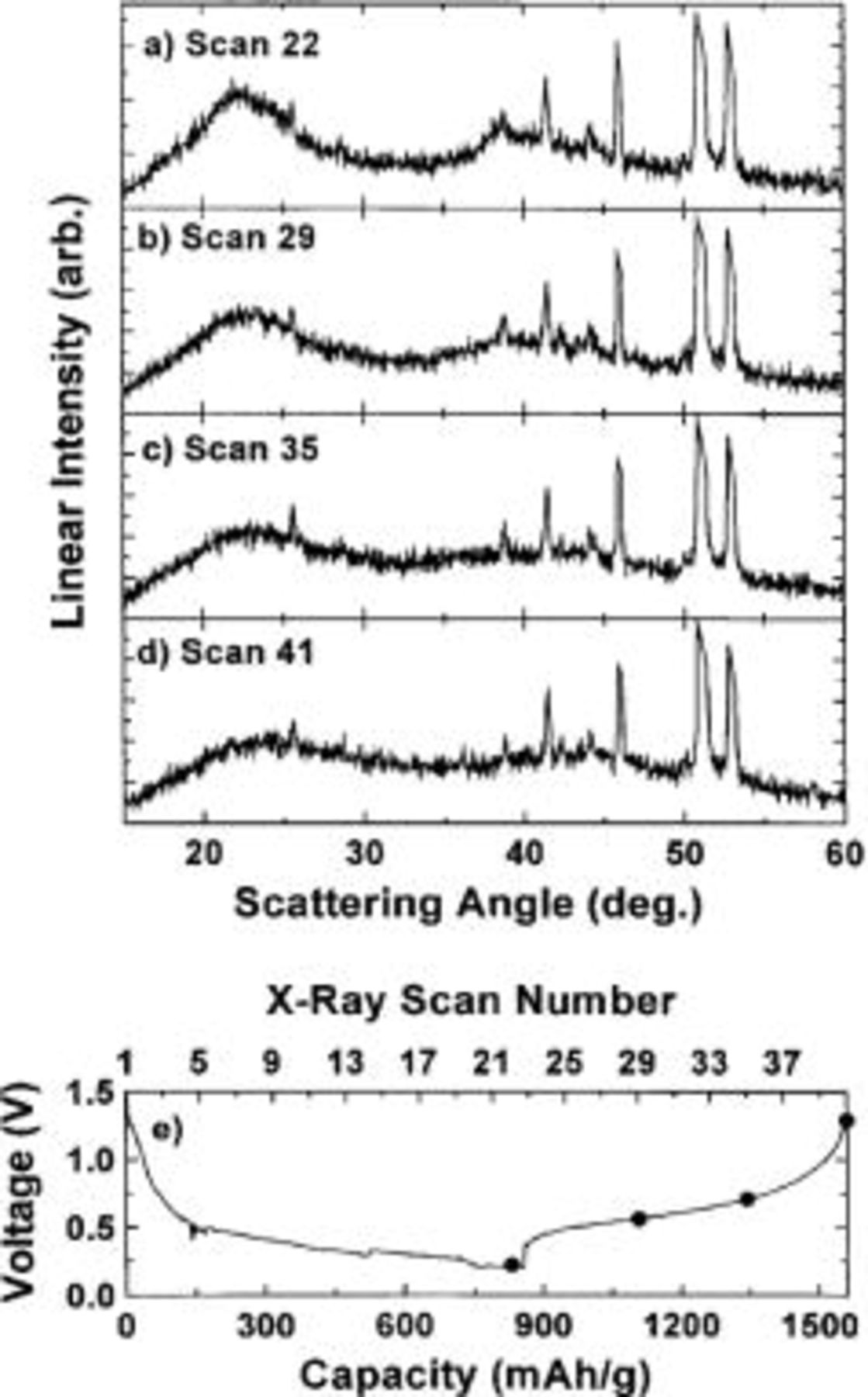
Figure 9. (a-d) In situ XRD patterns collected during the first charge cycle of a  electrode cycled against Li metal charge to 1.3 V. The sharp peaks in the diffraction patterns come from various cell parts. (e) Voltage vs. capacity (bottom abscissa) and X-ray scan number (top abscissa) collected during the experiment. (•) Indicates where the X-ray scans began.
In this same experiment in situ XRD patterns were collected for the second cycle where this time the cell was discharged to 0 V (approximately  in
in  . The results for the second discharge and charge cycle are shown in Fig. 10 and 11, respectively. The same gradual increase in broad peaks at
  and 40° (Fig. 10 b-d) are observed during the discharge. The 23° peak (shown in Fig. 10d) becomes more intense than the corresponding peak formed during the first discharge cycle (to 0.2 V) shown in Fig. 7d, presumably due to the larger amount of lithium added to the sample. Figure 11a-d shows that as lithium is again removed from the electrode the 23 and 40° peaks slowly disappear.
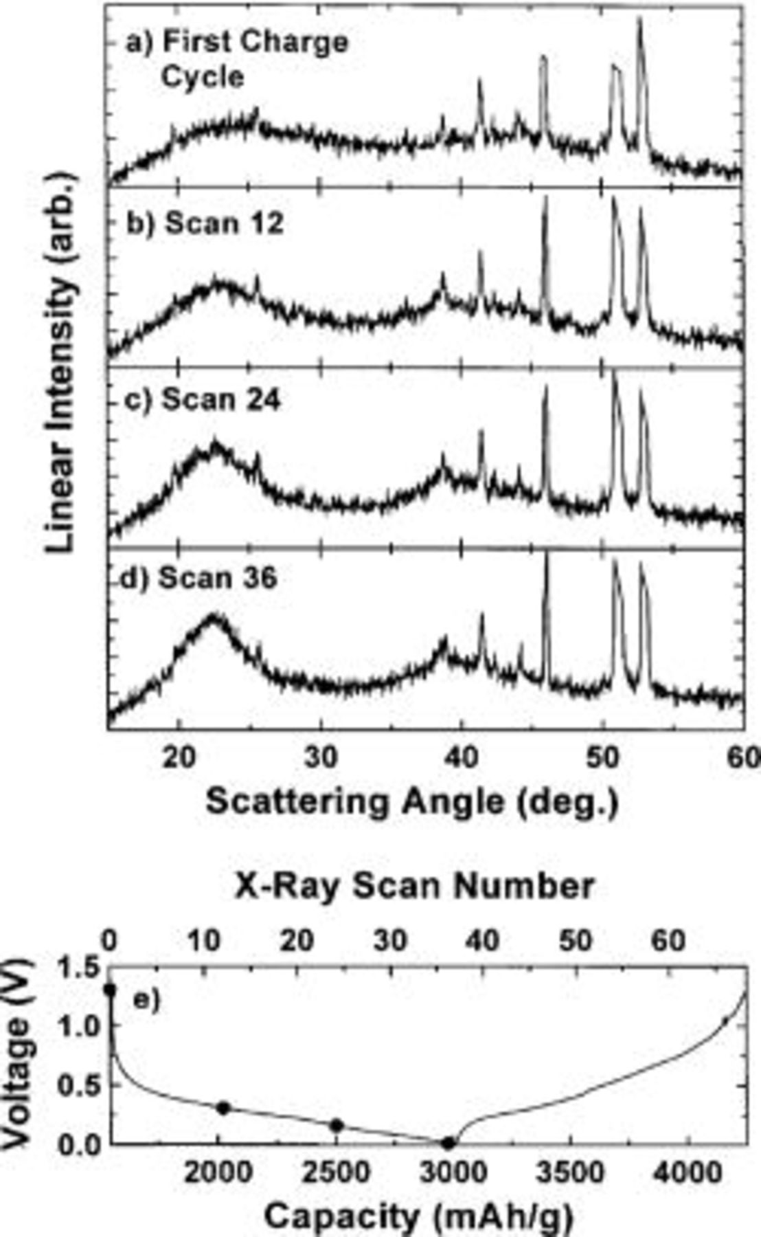
Figure 10. (a-d) In situ XRD patterns collected during the second discharge cycle of a  electrode cycled against Li metal to 0 V. The sharp peaks in the diffraction patterns come from various cell parts. (e) Voltage vs. capacity (bottom abscissa) and X-ray scan number (top abscissa) collected during the experiment. (•) indicates where the X-ray scans began.
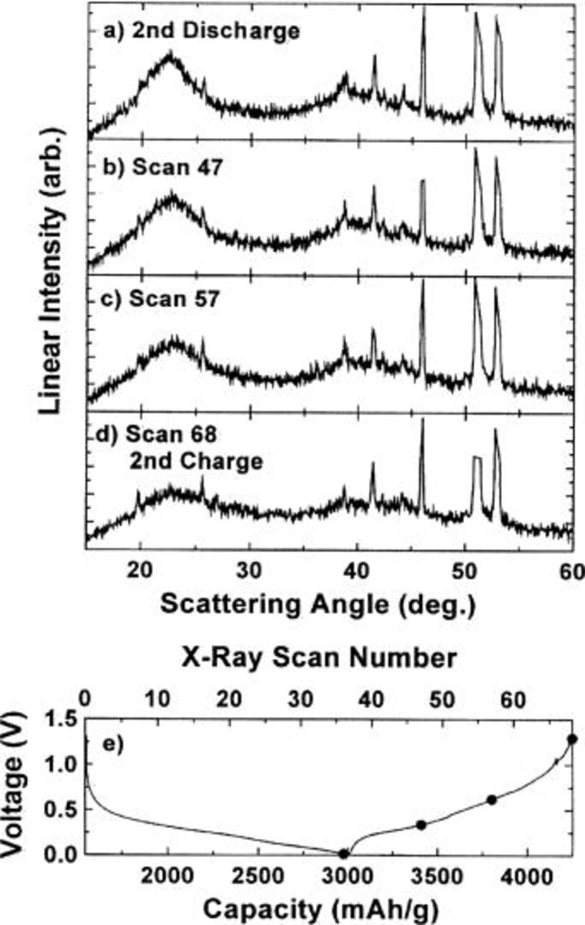
Figure 11. (a-d) In situ XRD patterns collected during the second charge cycle of a  electrode cycled against Li metal charged to 0 V. The sharp peaks in the diffraction patterns come from various cell parts. (e) Voltage vs. capacity (bottom abscissa) and X-ray scan number (top abscissa) collected during the experiment. (•) Indicates where the X-ray scans began.
The XRD pattern observed at 0 V (Fig. 10d) is very similar to that found during the room-temperature lithiation of Sn at the same potential.9 Figure 12 shows a comparison between the XRD pattern of a fully discharged  electrode (Fig. 12a), and a simulated XRD pattern of a Li-Sn tetrahedron (Fig. 12b). Such local tetrahedral arrangements of Sn atoms are found in
  and
and  where a Li atom is at the center of the tetrahedron and Sn or Si atoms are at the four corners. The edge length of the tetrahedron was taken to be 3.3 Å, approximately the same as the nearest neighbor Sn-Sn distance in
  The similarities between the two diffraction patterns are striking, suggesting that the local arrangements of Si and Sn atoms are similar to the local arrangements found in
  and
and 
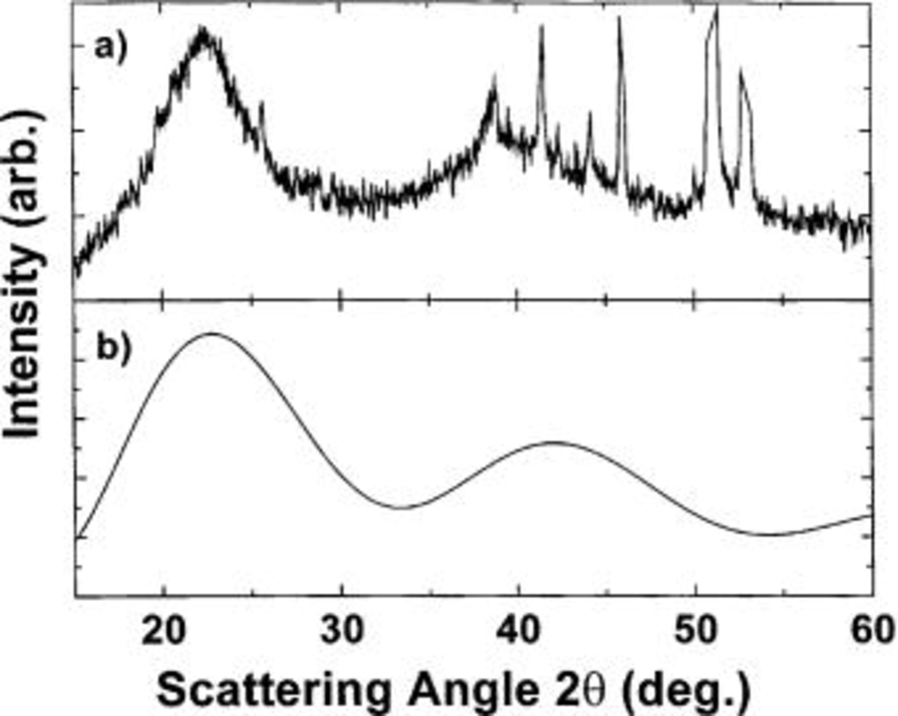
Figure 12. Comparison between the XRD pattern of (a) the fully discharged cell at 0 V and (b) the simulated XRD pattern of a Li-Sn tetrahedron of the type found in 
Figure 13 shows by XRD that the starting  material is structurally different from the final lithiated material,
  However, the intermediate diffraction patterns in Fig. 7, 8, 10, and 11 appear by eye to be made up of a fraction of the pattern from the first scan of the cell (Fig. 7a) and a fraction of the pattern from the electrode at 0 V, Fig. 10d. In order to examine this idea more fully, we represented an arbitrary scan of the electrode in the cell,
  as a sum

where  is the calculated
  th data point of the
  scan,
scan,  is the
  data point of the fresh cell scan (Fig. 7a),
  is the
  data point of the scan at 0 V (Fig. 10d), and z is a number between 0 and 1. The index, m, runs from 1 to M, where M is the number of data points in each scan, in this case 900. The goodness of fit,
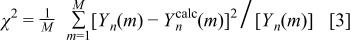
  defined as
was then minimized (using the solver feature of Microsoft Excel) by changing z. Figure 14 shows some fits to data sets based on this approach. For example, Fig. 14a shows that scan 11 of the first discharge is well fitted with  Fig. 14c shows that scan 22 of the first discharge (Fig. 7d) is well fitted with
  and Fig. 14e shows that scan 31 of the first cycle, during charge, is well fitted with
  For the second cycle, Fig. 15a shows that the first scan of the second discharge (scan 41 overall) is well fitted with
  Fig. 15c shows that scan 18 of the second discharge (scan 58 overall) is well fitted with
  and Fig. 15e shows that scan 51 (scan 92 overall) of the second cycle, during charge, is well fitted with
  In fact, almost all the scans can be fitted well by this approach as we show later.
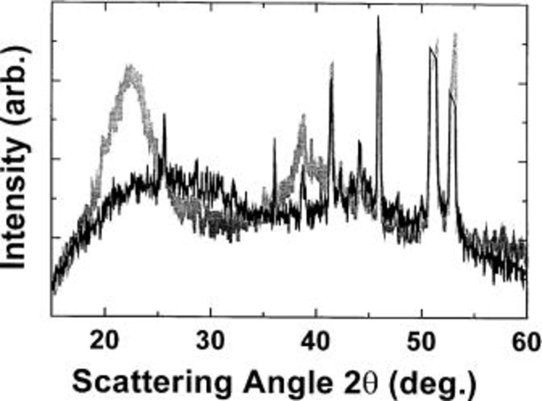
Figure 13. Comparison between the XRD pattern of the (dark line) fresh cell and (light line) the fully discharged cell (0.0 V), corresponding to 
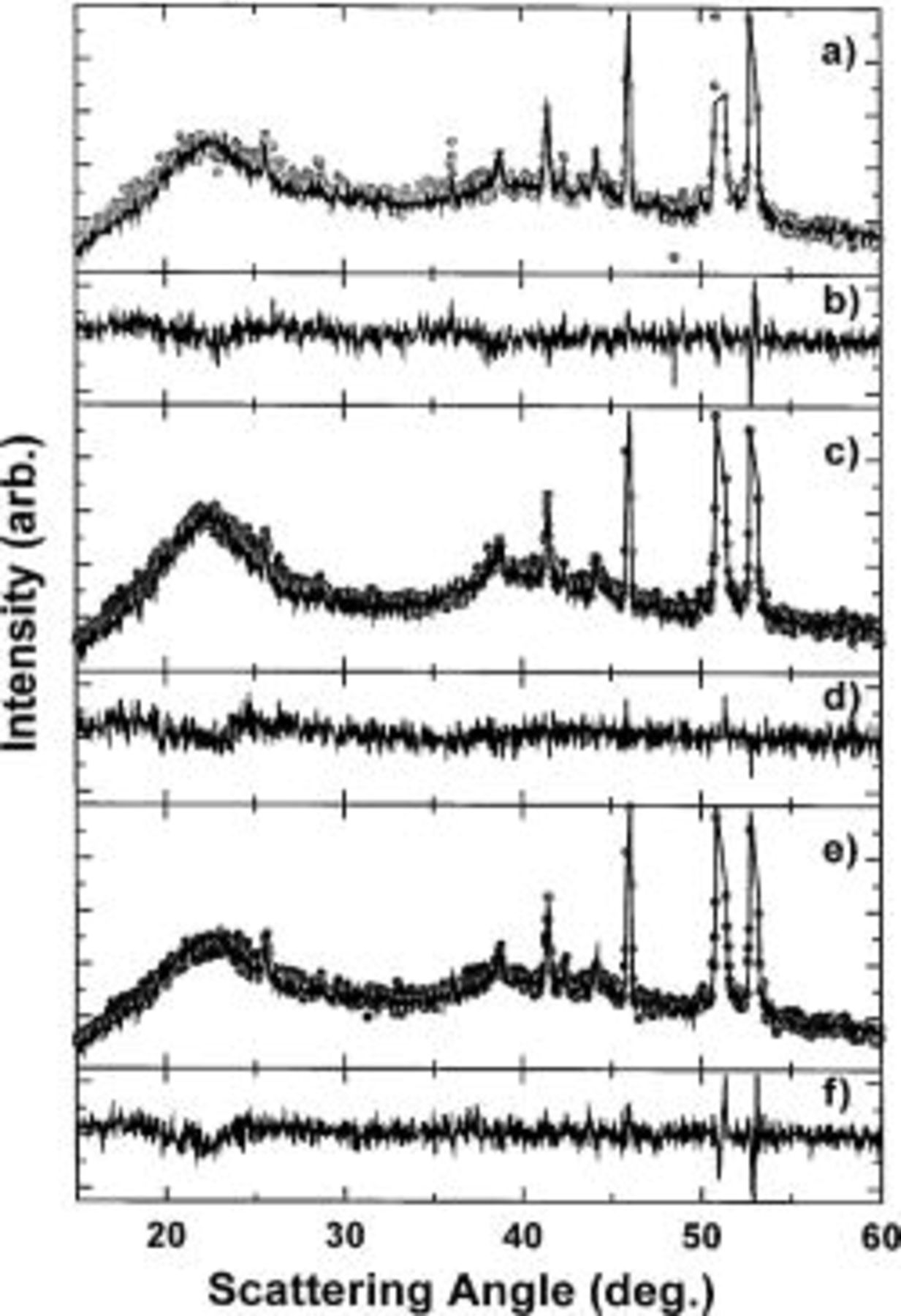
Figure 14. (a) (•) The XRD pattern of scan 11 of the first discharge cycle, while (—) shows the fit to the data set using a linear combination of the first scan and the scan taken at 0.0 V corresponding to  (b) Difference between scan 11 and the linear combination. (c) (•) The XRD pattern of scan 22 of the first discharge cycle, while (—) shows the linear combination. (d) Difference between scan 22 and the linear combination. (e) (•) The XRD pattern of scan 31 of the first charge cycle, while (—) shows the linear combination. (f) Difference plot between scan 31 and the linear combination.
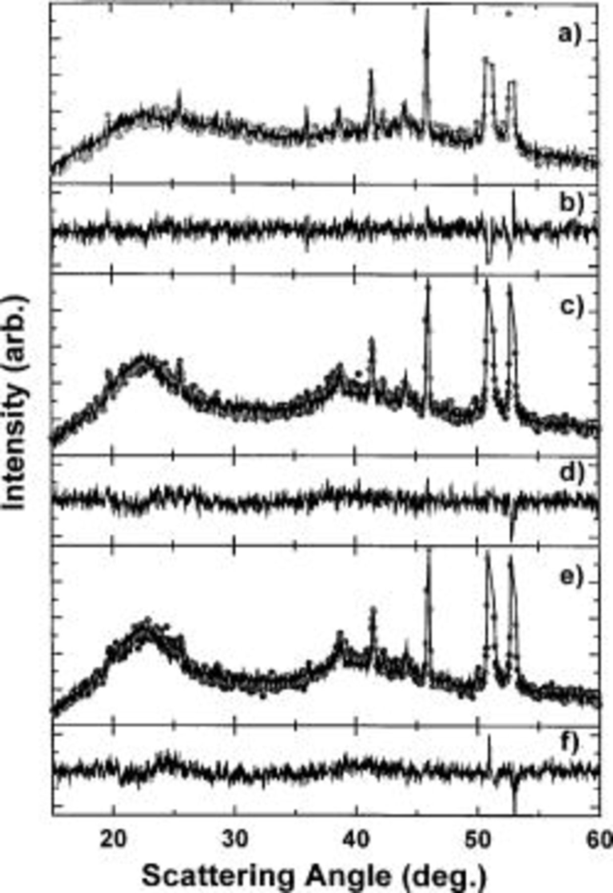
Figure 15. (a) (•) The XRD pattern of scan 1 (scan 41 overall) of the second discharge cycle, while (—) shows the linear combination. (b) Difference between scan 1 and the linear combination. (c) (•) The XRD pattern of scan 18 (scan 58 overall) of the second discharge cycle, while (—) shows the linear combination. (d) Difference between scan 18 and the linear fit. (e) (•) The XRD pattern of scan 51 (scan 92 overall) of the second charge cycle, while (—) shows the linear combination. (f) Difference between scan 51 and the linear combination.
Figure 16a shows the cell potential vs. scan number, n, for the first two cycles, Fig. 16b shows  vs. n, and Fig. 16c shows both z and
  vs. n. Since we are fitting a data set with random statistical noise by the linear combination of two other data sets having random statistical noise, a "perfect" fit will have
  (If a data set with random statistical noise is fit to a noise-free calculation, then it is well known that a "perfect" fit will have
  In our case, a perfect fit has
  because the calculated curve and the data set both have statistical noise.) Figure 13b shows that the fits give
  near 2 for most of the data sets, proving that all scans can be well represented by a linear combination of the scan from the fresh cell and the scan from the fully discharged cell.


Figure 16c shows that as x in  increases, the diffraction pattern shows more and more evidence of the local structure found in
  Sn or
Sn or  Si, since z increases when x increases. When the lithium is removed from the electrode, the diffraction pattern reverts to that characteristic of the local structure found in the diamond lattice. The variation of z and
  with scan number, or x, is not perfectly linear. For example, there is a region in Fig. 16c, near the start of the experiment, when z does not change appreciably for the first three scans. This may indicate that either the transferred lithium is consumed by irreversible surface reaction and is not incorporated into the host, or that the transferred lithium is incorporated uniformly interstitially within the diamond-like
  structure without causing significant bond rearrangements as found in
  Sn. In the range from scans 60 to 78 in Fig. 16c, the variation of z with scan number slows. The local structure of Sn and Si atoms found in
  Sn or
Sn or  Si may be predominantly formed at smaller lithium concentrations (say near
  and hence z would approach 1 as observed. Adding further lithium would not impact the diffraction pattern significantly, since its scattering power is small, if the correct local arrangement of Si and Sn atoms has already been established.
This in situ XRD experiment clearly shows the room-temperature electrochemical reaction of Li with this  electrode proceeds via a relatively benign exchange reaction of the local environment of
  for the local environment of
  nce the materials remain amorphous at all times during cycling and since there are no plateaus in the voltage-capacity relation, it can only be assumed that these two local environments are distributed evenly throughout the bulk of the material. This reaction mechanism is perhaps the main factor contributing to the favorable cycling performance of this compound. This is discussed further in upcoming publications.
Finally, now that the reaction process is understood, it is possible to make some statements about the origin of the hysteresis between charge and discharge displayed in Fig. 6. Figure 17 shows the voltage vs. capacity for two  cells cycled at 55 and 30°C at different current densities. In order to see the hysteresis more clearly, the voltage curves have been normalized to the same capacity during charge and discharge. The true discharge capacity has been plotted, and the charge curve has been scaled to have the same capacity. From this data, the difference in the average voltage between the charge and discharge cycle was measured for each charge cycle. This data is plotted in Fig. 18 against the specific current. As expected, the hysteresis of the 55°C cell is less then the hysteresis of the cell cycled at 30°C. The hysteresis of the cells does not approach zero as the current density approaches zero. Therefore, the hysteresis is inherent and the area between the charge and discharge curves represents the energy dissipated during one charge-discharge cycle. We speculate that the energy is dissipated by the changes in the local atomic environment around the host atoms that involve the breaking and creation of new bonds involving the host atoms and lithium. Using the results in Fig. 17 and 18, we can estimate the magnitude of the energy dissipated by the hysteresis. Figure 18 shows that the offset between charge and discharge is about 0.2 V. Figure 17a, for the lowest charge-discharge rate, gives a capacity of about 4 Li atoms per
  Therefore, the hysteresis energy is about 0.8 eV per
  formula unit. Since chemical bonds generally have energies on the order of a few electronvolts per bond, we feel that the measured energy is consistent with a change in the local environment of the Si and Sn atoms.
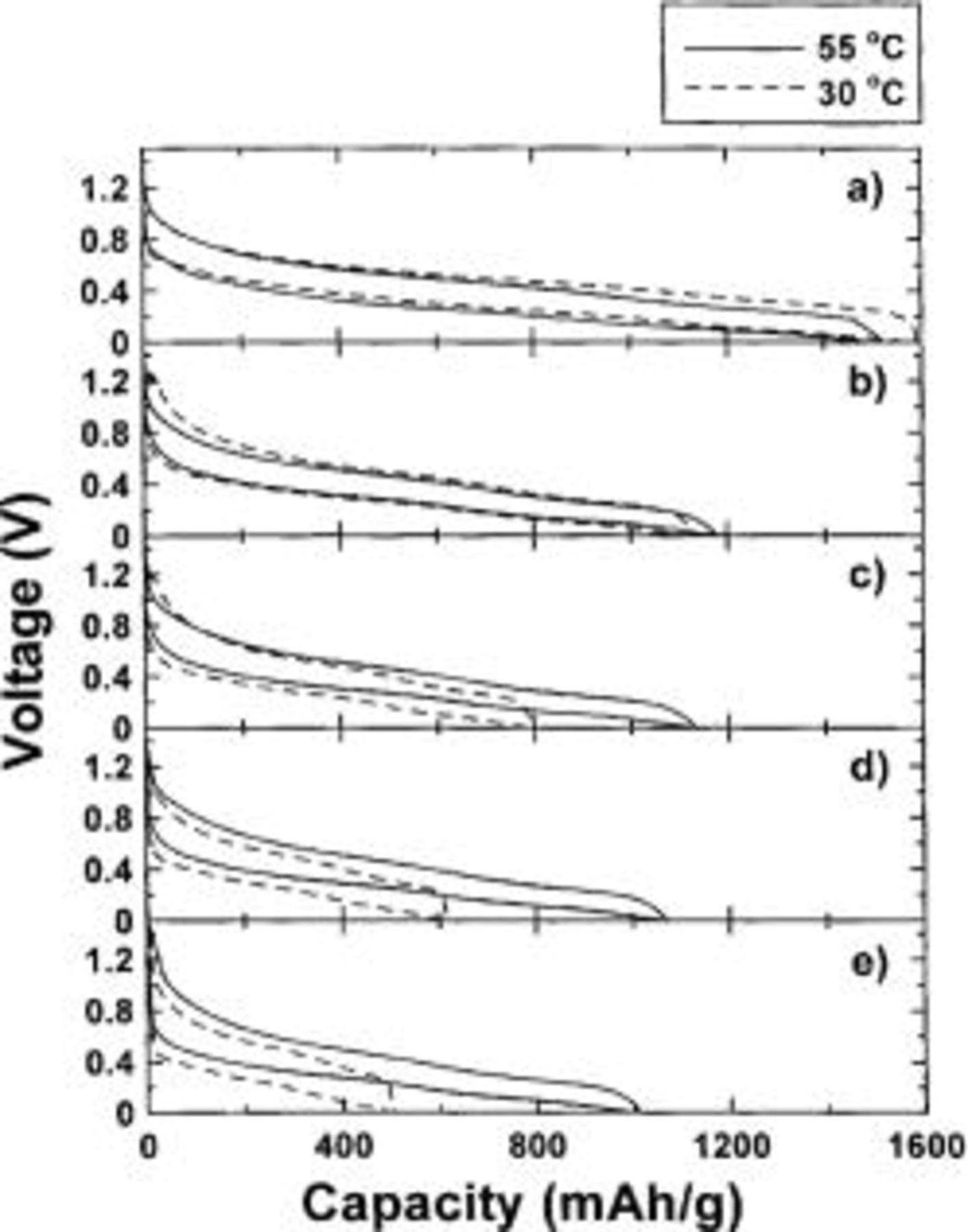
Figure 17. Graph of voltage vs. capacity of two cells cycled at (—) 55 and (---) 30°C. All voltage curves have been normalized. Specific current of the 55°C cell is (a) 14.3, (b) 28.6, (c). 57.0, (d) 114.4, and (e) 228.6 mA/g. Specific current of the 30°C cell is (a) 16, (b) 33, (c) 66, (d) 133, and (e) 266 mA/g. The factors used in the normalization of the voltage curves of the 30 and 55°C cells are, respectively, (a) 1.62 and 1.44, (b) 1.12 and 1.18, (c) 1.08 and 1.10, (d) 1.06 and 1.07, and (e) 1.04 and 1.02. The normalization factors are largest at the smallest currents due to inaccuracies in the currents from the chargers at currents below 10 mA.
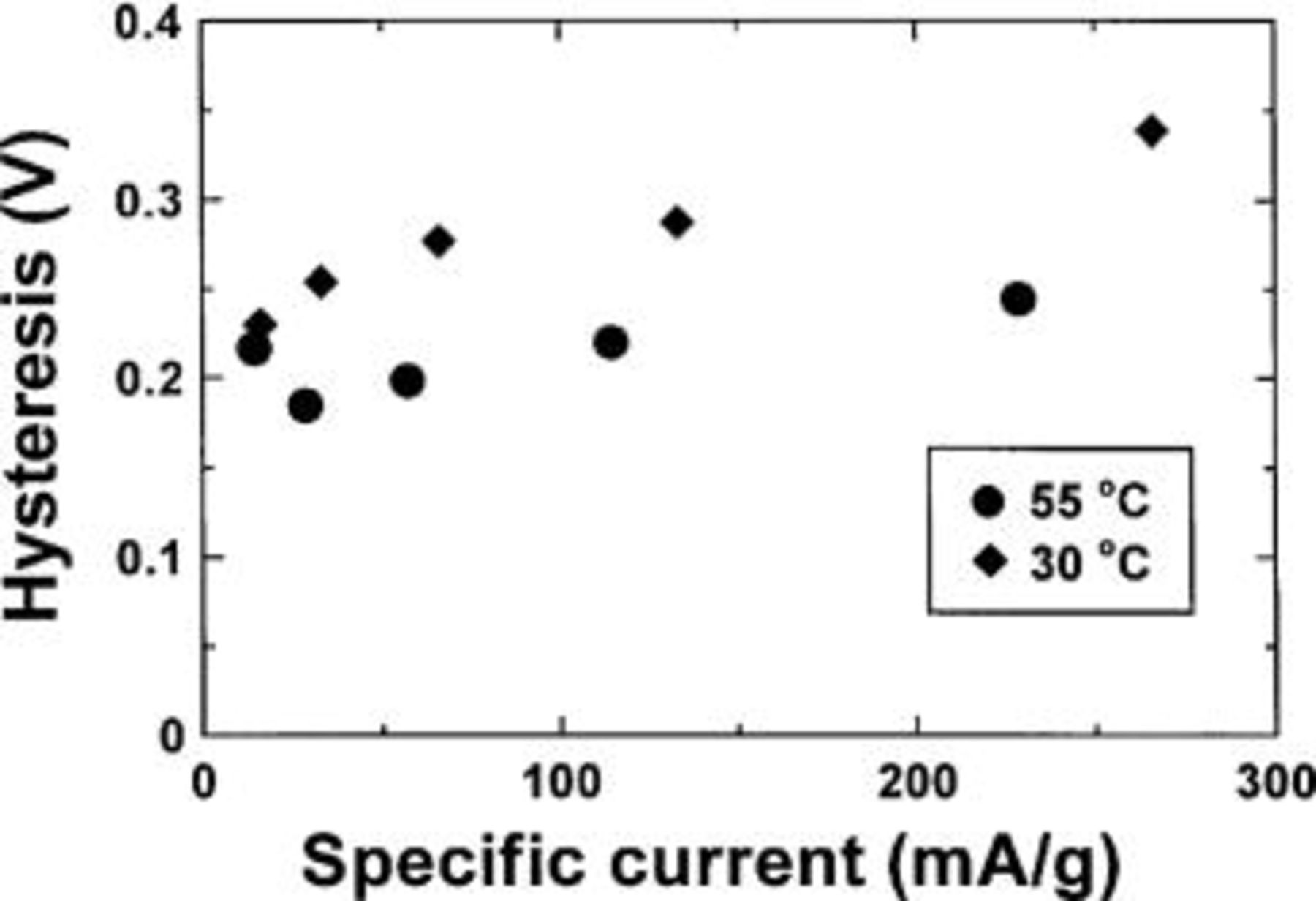
Figure 18. Hysteresis voltage vs. specific current of two cells cycled at (•) 55 and (♦) 30°C.
Conclusion
We have shown that  samples for
  can be prepared by magnetron sputtering using a combinatorial materials science approach. Resistivity and XRD measurements were used to screen the composition range and indicated the most promising sample to be
  Electrochemical and in situ XRD experiments have shown predominantly only two local environments for Si and Sn are found at any value of x in a-
 nce the materials remain amorphous at all times during cycling and since the voltage profile is smooth, it can only be assumed that the two local environments are distributed evenly throughout the bulk of the material. This reaction mechanism is believed to be the reason that a-
 can undergo reversible colossal volume expansion as we have shown earlier.4
Acknowledgments
The authors acknowledge the support of parts of this research by the Natural Sciences and Engineering Research Council (NSERC) of Canada. L.Y.B. would like to thank NSERC, 3M, and 3M Canada for scholarship support.
Dalhousie University assisted in meeting the publication costs of this article.