
Abstract
Requirements of transparent-conductive oxide (TCO) films for solar cells and other optoelectronic applications are mainly focused on the electrical resistivity as low as  , optical transmittance above
  in the visible region, a long-term stability in damp heat-treatment for 1000 h, a mechanical stability on flexible polymer substrates, and the large-area deposition technique for commercialization. In this study, the typical properties of the 45 nm thick Al-doped ZnO (AZO)/Ag/45 nm thick AZO multilayer films embedded by silver layers with various thicknesses were addressed to satisfy the requirements of TCO films for flexible electronic device applications. The AZO/9 nm thick Ag/AZO multilayer films as deposited on poly(ether sulfone) (PES) polymer substrates at
  by radio-frequency magnetron sputtering, which the deposition on large-area substrates is possible, exhibited the electrical resistivity of approximately
  , optical transmittance of 88% at 550 nm wavelength, no appreciable change in electrical resistance and optical transmittance after damp heat-treatment for 1000 h, and a strong mechanical stability between multilayer films and PES substrates after a severe bending test. The results presented in the multilayer films can provide a platform for TCO films deposited on polymer substrates to enable the flexible electronic device applications.
Export citation and abstract BibTeX RIS
Transparent-conductive oxides (TCOs) are widely used in many thin-film devices depending on the conductivity and transmittance. The most common materials used for the production of transparent-conductive films are doped metal oxides, for example,  ,
,  (ITO), and ZnO:Al. Al-doped ZnO (AZO) thin films show low electrical resistance and high transmittance in the visible range of the spectrum for the applications of transparent-conductive electrodes in optoelectronics devices including flat displays, thin-film transistors, and solar cells.1–3 They have properties of transparent electrodes comparable to Sn-doped
  with a resistivity as low as
  and an optical transmittance of
  in the visible region. They cost less in raw material and have good thermal stability; moreover, they are more stable in a hydrogen plasma ambient than ITO4–6 and thus, many studies have concentrated on replacing ITO with AZO films. The electronic conductivities of TCOs are needed in optoelectronic device applications such as flexible organic light-emitting diodes (sheet resistance
  ) and plasma display panel optical filter
  . However, AZO films themselves have not shown enough electrical conductivity for both applications until now. To increase the electronic conductivity and retain the high transmittance, development of a certain range of multilayer coating consisting of three to five alternative layers of metal and semiconductor or dielectrics is investigated.7, 8 Earlier transparent metal electrodes of gold, silver, and copper in very thin forms, approximately up to 15 nm thick, were used in early optoelectronic devices.9 However, simultaneous optimization of conductivity and transparency presents a considerable challenge in film deposition. Some authors reported that ITO/Ag/ITO may be used to surpass ITO for higher conductivity and lower cost.10–12 Because of the extremely high target cost of ITO, AZO13–15 is well known as the most potential candidate to substitute ITO film. The silver film-coated AZO16 and AZO/Ag/AZO multilayer films17 have been studied to improve the electronic conductivity and the high transmittance because Ag has a low resistivity of approximately
  . Most of the silver-based AZO films deposited on the glass substrates at a low temperature
  showed a low optical transmittance in the visible wavelength range16, 17 even though they exhibited a low resistivity (sheet resistance of
  ) compared to the AZO films. These results still remain the stumbling blocks for the integration of silver-based AZO films on the flexible devices. The optical properties of very thin metal films depend considerably on their structure.18 Accordingly, it is important to optimize the condition of deposition process for practical use of TCO.
Recently, an important issue in the field of photovoltaic solar cells was presented to prepare solar modules with a long lifetime in harsh outdoor conditions. AZO films are employed as front contacts for silicon or  -based thin-film solar cells.19–21 To realize the commercialization of thin-film solar cells, a good long-term damp-heat stability of solar cells is required. Here, degradation is enforced by damp heat-treatment in conditions similar to the IEC 1646 Standard (85% relative humidity at
  for 1000 h).22 The sheet resistances of the AZO films crystallized at room temperature by radio-frequency (rf) magnetron sputtering increase due to the decrease in carrier concentration and mobility during the damp heat-treatment.23 The degradation of electrical properties was due to the oxygen and water molecules penetrated into the films via the defect paths.24
Here, for the TCO available in the flexible electronic device applications, we address the optimum electrical resistivity and a transmittance of AZO/Ag/AZO multilayer films deposited on poly(ether sulfone) (PES) polymer substrates by rf magnetron sputtering on which the deposition on large-area substrates is possible. The mechanism for a good long-term damp-heat stability of the multilayer films was addressed for the commercialization of the TCO films. For the applications of TCO on flexible polymer substrates, flexibility of the TCO was also presented through the severe bending test.
Experimental
AZO thin films were grown on PES polymer substrates by rf magnetron sputtering from a  ceramic target (2 wt %
  ). For the deposition of AZO and Ag films, the target-substrate distance was 110 mm and the base pressure in the sputtering chamber was
  . Argon gas (20 sccm) was introduced in the sputtering chamber with a sputtering pressure of 0.13 Pa. The AZO and Ag films were grown at
  with sputtering power densities of 4.1 and
  . For the deposition of the multilayer structure, initially AZO films were deposited on PES at
  . Without breaking the vacuum, Ag films were deposited on the AZO/PES at a substrate temperature of
  . Finally AZO was deposited on Ag/AZO/PES at a substrate temperature of
  in the same vacuum condition. The decision of the ultrathin Ag film thickness deposited on AZO/PES was performed with a deposition rate [thickness was measured by scanning electron microscopy (SEM) cross-sectional images] of Ag deposited on the AZO/glass. Conventional
  X-ray diffraction (XRD) studies on the films were carried out in a Rigaku (D/Max 2500) diffractometer using
  radiation to investigate the crystallinity and crystal orientation of the films. The surface images of Ag layers with various thicknesses were investigated by scanning electron microscope, and the continuous nature of the Ag midlayers in the AZO/Ag/AZO multilayer was identified by transmission electron microscope. The sheet resistance was measured using a four-point probe method within an accuracy of
  . The carrier concentration and carrier mobility of multilayer films were measured using a van der Pauw method. The optical transmittance of multilayer films was measured in the wavelength range of 300–800 nm by using a spectrophotometer. The damp-heat test of 45 nm thick AZO/9 nm Ag/45 nm thick AZO and 100 nm thick AZO films was performed at the conditions of
  temperature and 85% relative humidity for several times. The bending test of the multilayer films experienced in the damp heat-treatment for 1000 h was performed as follows: One side of the
  sample was fixed and the other side was pushed. The schematic diagram for the bending test is shown in the inset of Fig. 5a. The samples bended at each point were maintained for 30 s. Variations in electrical resistance and the surface images of the samples after bending at each point were measured by a four-point probe method and an optical microscope.

Figure 5. The variations in (a) electrical resistance and (b) the optical images as a function of bending length. The samples are 45 nm AZO/9 nm Ag/45 nm AZO films experienced in the damp heat-treatment for 1000 h. The inset in (a) is a schematic diagram for the bending test.
Results and Discussion
The crystalline phase, crystalline size, and crystallinity of the AZO films as a function of thickness of the silver layer were investigated by  , Scherrer formula,25 and ω scans of XRD. The
  patterns of AZO films as a function of thickness of the silver layer are shown in Fig. 1a. The AZO films were grown with (002) preferred orientation, and Ag(111) peaks above 3 nm thick Ag layers were also observed in the sandwiched structure of 45 nm thick AZO/Ag/45 nm thick AZO. The inset in Fig. 1a shows the crystalline size of the AZO multilayer films as a function of Ag layer thickness and shows the distribution of the crystalline size of 6–8 nm. The crystallinity of the multilayer films was identified using full width at half-maximum (fwhm) values calculated by rocking curves and was shown in the inset of Fig. 1b. The crystallinity of the AZO films grown on continuous Ag midlayers is higher than the single AZO films without the Ag layer. From the analysis of the crystalline structure, AZO multilayer films with continuous Ag midlayers are expected to exhibit the excellent electrical properties for the flexible electronic device applications. The microstructures of the Ag layers on AZO films and the Ag midlayers embedded in the AZO multilayer are investigated by SEM and high resolution transmission electron microscopy (TEM) images, and are shown in Fig. 2. Figure 2 shows SEM surface images of (a) 3, (b) 9, and (c) 20 nm thick Ag layers on AZO films and the high resolution TEM images of (d) AZO/3 nm thick Ag/AZO, (e) AZO/9 nm thick Ag/AZO, and (f) AZO/20 nm thick Ag/AZO structures. As shown in Fig. 2a and 2d, 3 nm thick Ag layers show discrete morphologies rather than the continuous natures. 9 nm thick Ag layers exhibit the homogeneous morphologies, indicating the films shown in Fig. 2b and 2e. The 20 nm thick Ag layers show similar morphologies to those of 9 nm thick Ag layers. The homogeneous morphologies of the silver layers inserted between the AZO layers basically influence the optical transmittance and the resistivity of the AZO-conducting oxide films on flexible polymer substrates. The relationship between Ag layer thickness and optical transmittance has been reported by many researchers.16, 17, 26, 27 They reported that the Ag-based AZO multilayer films exhibit the reduced optical transmittance in the range of visible wavelength even though the multilayer films have a low sheet resistance of approximately
  .17 The transmittance spectra observed for different thicknesses of the silver layer in the AZO/Ag/AZO multilayer are placed in Fig. 3a. The transmittance spectra of 100 nm thick AZO films are also shown in Fig. 3a. There is an increase in transmittance with an increase in thickness of silver from 3 to 9 nm. With further increase in thickness of the Ag layer, a decrease in transmittance is observed. The maximum transmittance peak was observed at approximately 550 nm wavelength for different silver thicknesses. The percentage of maximum transmission of the AZO multilayer as a function of silver layer thickness is presented in Fig. 3b. The maximum of transmittance in the visible spectrum was considered because this value is independent of the interference phenomena associated with multiple reflections of the film and is indicative of their optical observation. As shown in Fig. 3b, the maximum percentage of approximately 88% in the AZO multilayer was observed at 9 nm thickness of the Ag layer. There is a decrease in the maximum percentage of transmittance with an increase or decrease in the Ag layer thickness beyond 9 nm. As shown in SEM and TEM images of 9 nm thickness of the Ag layer, an increase in the optical transmittance in the AZO multilayer with a continuous Ag layer can be explained by a propagating surface-plasmon resonance.28 The continuous layer of 9 nm thick inserted between the AZO layers produces the effect of amplification of electric field within the AZO layers by metal surface-plasmon resonance, which occurred by a grouped vibration of electrons existing within the silver metal. As a result, a considerable increase in the optical transmittance in the AZO multilayer was attributed to the optimum thickness of the continuous Ag layer. In the AZO/Ag/AZO multilayer, an optimum thickness of the continuous Ag layer is required to display effectively the effect of surface-plasmon resonance. As shown in Fig. 3b, with the increase in the thickness of the Ag layer beyond 9 nm, it behaves like a reflecting mirror, so there is more reflection of light and less transmittance. Therefore, transmittance decreases and reflection increases with further increase in silver thickness. As shown in Fig. 2a and 2d, silver layers of 3 nm thick look like distinct islands of silver atoms, and the aggregated state of the silver atoms rapidly increases the absorption of light, as reported results,10 resulting in a decrease in transmittance. Figure 3c shows the variations in resistivity, carrier concentration, and Hall mobility of AZO multilayer films as a function of Ag layer thickness. The carrier concentration and the mobility decrease and increase, with increasing Ag layer thickness. As shown in Fig. 3c, AZO multilayer films with 3 nm thick Ag layer show an unusual behavior in terms of the carrier type and resistivity. The multilayer films inserted by a Ag layer above 5 nm thick exhibit a slight decrease in the resistivity with increasing Ag layer thickness. The AZO multilayer with a Ag layer thickness of approximately 9 nm exhibits the resistivity of about
  . To assist the selection of the AZO multilayer produced concerning their application on optoelectronic devices, we determine the figure of merit
  defined as29
  , where
  is the transmittance of the multilayer on 550 nm wavelength and
  is the sheet resistance of the multilayer. In most cases, the maximum transmission is required at 550 nm where the human eye has its maximum sensitivity. Figure 3d shows the variations in
  of the AZO multilayer for different Ag layer thicknesses. The AZO multilayer with 9 nm thick Ag layer has the best electrical performance of approximately
  . The electrical merits of 45 nm thick AZO/9 nm thick Ag/45 nm thick AZO multilayer exceed much developed transparent conductive films (
 26 and
  30).
30).
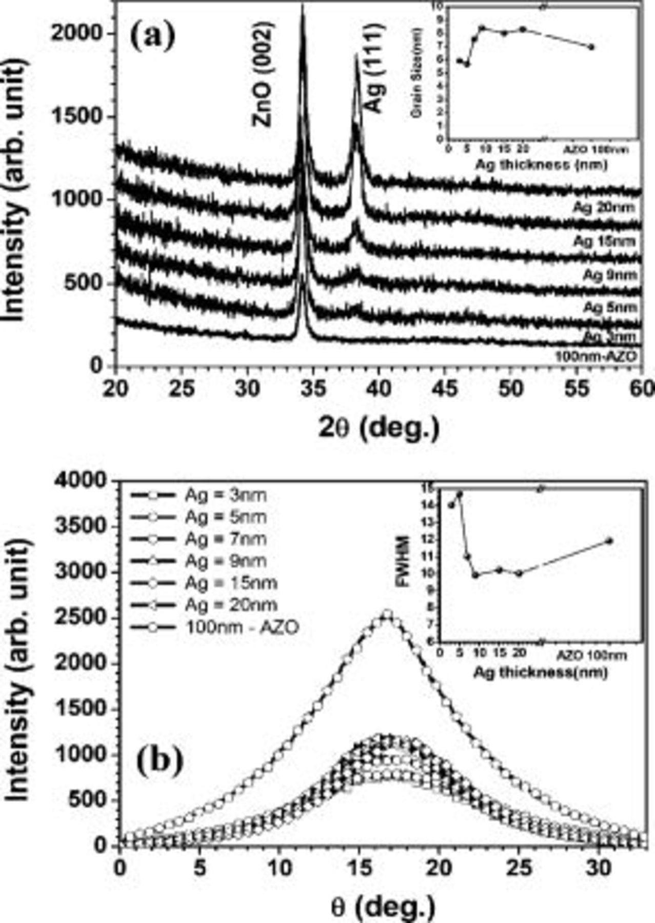
Figure 1. (a) XRD  patterns of AZO multilayer films as a function of Ag midlayer thickness and 100 nm thick AZO single layer films grown on PES substrates. Inset in (a) shows the variations in crystalline size as a function of Ag layer thickness and AZO single layer films. (b) XRD ω scans of AZO multilayer films as a function of Ag midlayer thickness and 100 nm thick AZO single layer films. Inset in (b) shows the fwhm values of AZO multilayer films as a function of Ag layer thickness and AZO single layer film.
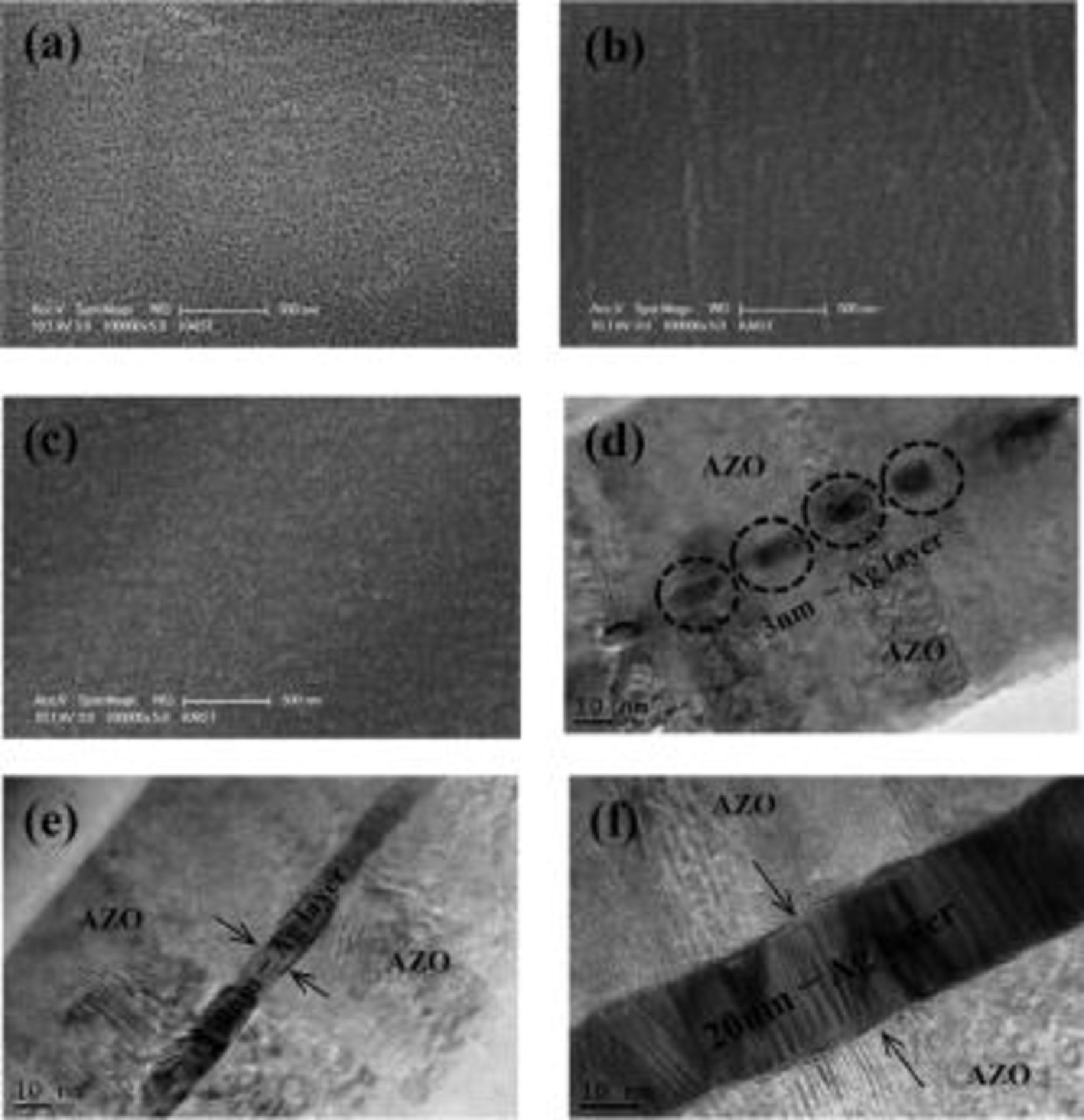
Figure 2. SEM surface images of (a) 3, (b) 9, and (c) 20 nm thick Ag layers deposited on AZO/PES and the high resolution TEM cross-sectional images of (d) AZO/3 nm thick Ag/AZO, (e) AZO/9 nm thick Ag/AZO, and (f) AZO/20 nm thick Ag/AZO structures.
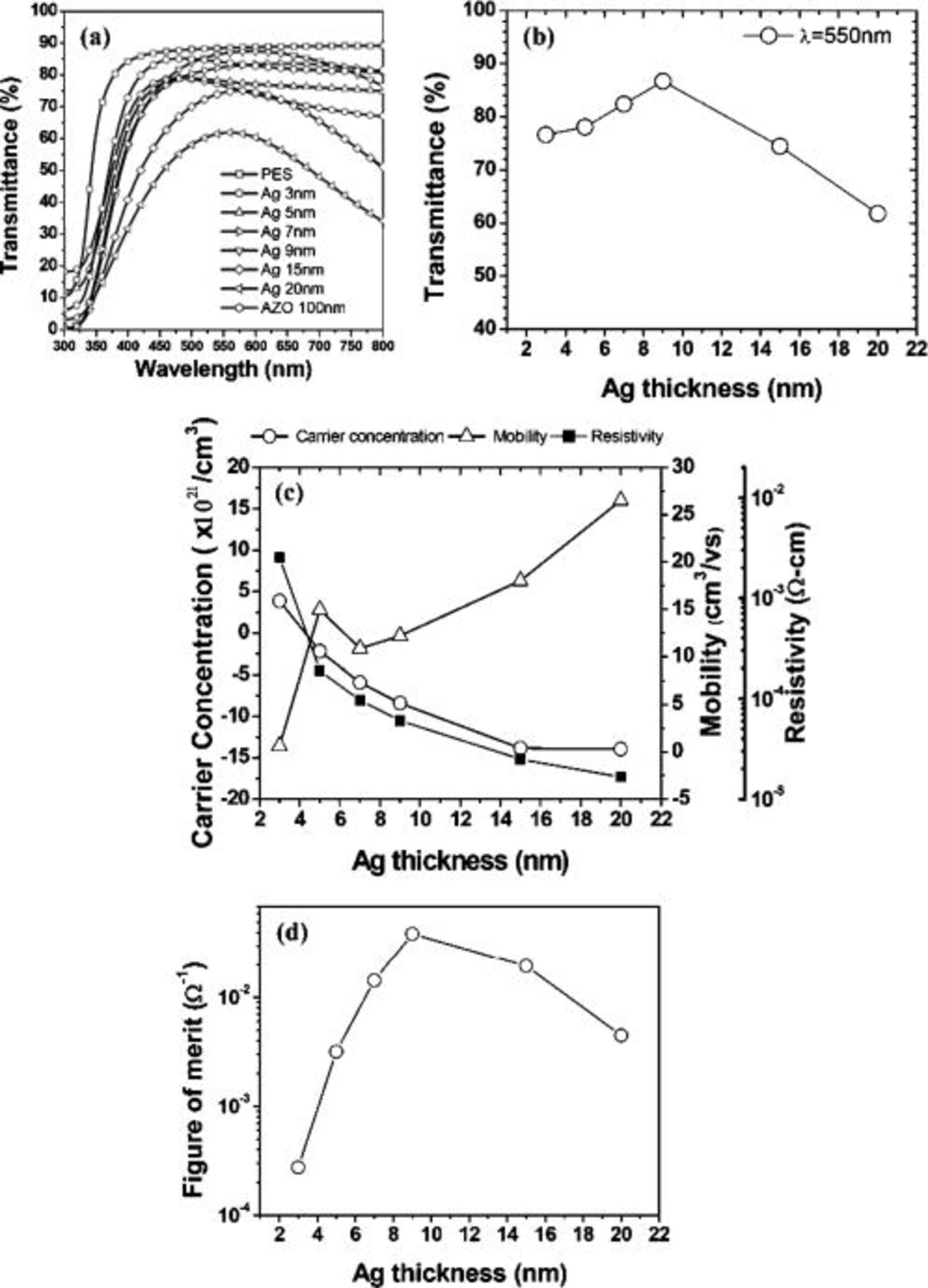
Figure 3. (a) Optical transmittance spectra observed for different silver layer thicknesses in AZO/Ag/AZO multilayer films and 100 nm thick AZO single layer films. (b) The percentage of maximum transmittance in AZO multilayer films as a function of silver layer thickness. (c) Variations in resistivity, carrier concentration, and Hall mobility of AZO multilayer films as a function of Ag layer thickness. (d) Variations in figure of merit  of AZO multilayer films for different Ag layer thicknesses.
The 45 nm AZO/9 nm Ag/45 nm AZO and the 100 nm AZO samples grown on PES polymer substrates have also been analyzed after exposition to the damp-heat conditions. The electrical resistances of both samples are plotted in Fig. 4a as a function of the treatment time. In AZO films, Lin et al.23 reported that the sheet resistance increase in all films varies in the range of 23–31%. The thickest AZO films (160–320 nm) show the smallest fluctuation in electrical properties, while the thinnest films (95 nm) are affected most by the damp heat-treatment. Guillén et al.24 also reported that the stability for the damp-heat conditions in the ITO films was achieved by an appropriate control of the film orientation from (222) to (400) crystallites. The predominance of (222)-orientated grains in the samples, which can accommodate a larger amount of interstitial oxygen atoms and show higher lattice distortion than the (400) crystallites, would be responsible for the lower stability against humidity ingress. As shown in Fig. 4a, AZO/Ag/AZO multilayered samples do not show an electrical degradation during the damp heat-treatment up to 1000 h, while AZO samples exhibit a severe degradation of the sheet resistance of approximately 66%. As shown in Fig. 4a, for AZO/Ag/AZO, samples deposited on Si(001) substrates exhibit a similar tendency to those on PES polymer substrates. This means that the degradation of the electrical resistance by a damp heat-treatment depends on the intrinsic effect of the AZO/Ag/AZO films. In AZO single-layered samples, the basic origin for the degradation of the electrical properties during the damp heat-treatment is known that the incoming oxygen and water molecules primarily penetrate via the defect paths; the smaller distortion of the semiconductor lattice and the smoother layer surface can provide higher stability against humidity.19, 31 In the AZO/Ag/AZO/PES structure, the electrical resistance of AZO depends on the carrier transport of the continuous Ag midlayer.32 Accordingly, even though the resistance of the top AZO layer was increased by a damp heat-treatment, no appreciable variations in the electrical resistance of the AZO/Ag/AZO samples will be detected if the variations in morphology of the Ag layer do not occur by oxygen, and water molecules penetrated during the damp heat-treatment. The cross-sectional TEM micrographs of AZO/Ag/AZO thin films after damp heat-treatment for 1000 h are shown in Fig. 4b. The continuous Ag midlayer still keeps the original state under the conditions of the damp heat-treatment. The variations in optical transmittance for various wavelengths and maximum transmittance at 550 nm wavelength in AZO/Ag/AZO and AZO films as a function of damp-heat time are shown in Fig. 4c and 4d. As shown in Fig. 4c, the samples after damp heat-treatment for 1000 h exhibited similar optical transmittances to samples before damp heat-treatment. The maximum transmittance  of 100 nm thick AZO single-layered films (see Fig. 4d) was constantly maintained with increasing damp-heat time up to 1000 h. For AZO/Ag/AZO films, the transmissions showed a slight decrease of
  after 800 h. This slight decrease after damp heat-treatment was also observed at AZO films reported by various groups23, 24 and was acceptable in optoelectronic device applications of TCO films.
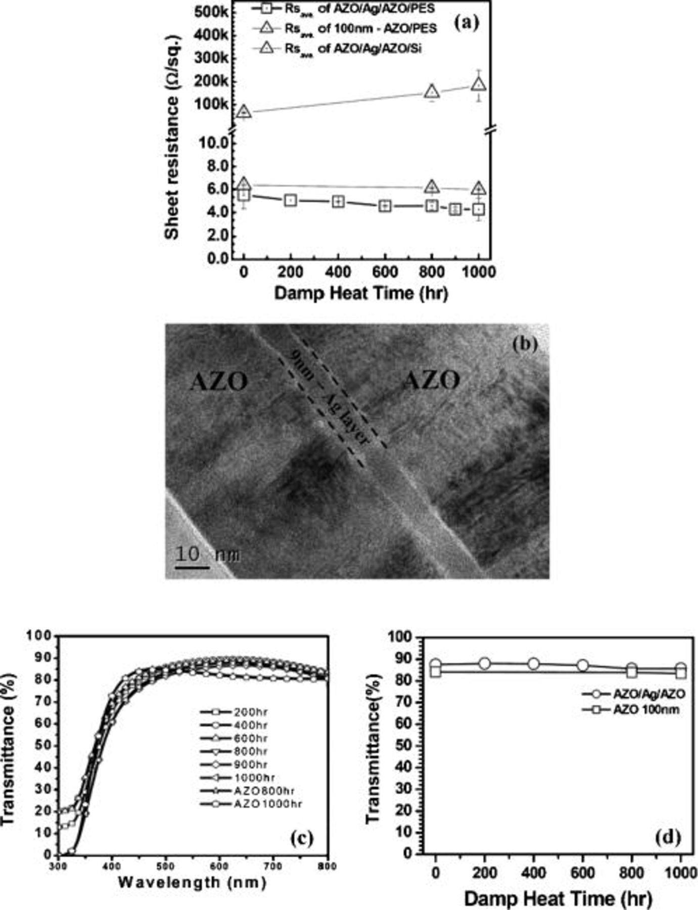
Figure 4. (a) Variations in electrical resistances in 45 nm AZO/9 nm Ag/45 nm AZO and the 100 nm AZO samples as a function of damp heat-treatment time. (b) Cross-sectional TEM micrographs of AZO/Ag/AZO multilayer films after damp heat-treatment for 1000 h. (c) Maximum transmittances at 550 nm wavelength in the AZO/Ag/AZO multilayer and 100 nm thick AZO single layer films as a function of damp-heat time.
Another requirement for TCO films deposited on flexible polymer substrates is a mechanical stability exhibiting a strong adhesion after bending test. In this paper, samples (AZO/9 nm Ag/AZO) performed for 1000 h under the conditions of damp heat-treatment were used for bending tests. The variations in electrical resistance and the optical images as a function of bending length are shown in Fig. 5a and 5b. The inset in Fig. 5a shows the schematic diagram for the bending test. The methods for the bending test are described in detail in the Experimental section. The sheet resistance values of the samples were measured after maintaining for 30 s at each bending position. The resistance values of the samples will be sensitively changed if they have minute cracks and a small removal of the films from the substrates after bending test. As shown in Fig. 5a, the sheet resistance values of the samples were constantly maintained within the error range as the extent of bending increases. The direct observation of the sample surfaces after bending test was performed by an optical microscope and their images are shown in Fig. 5b. Any appreciable variations in sample surfaces were not observed after bending test at each point. The spots observed on the images are attributed to the tints created by a four-point probe when the sheet resistance of the samples was measured. The results of a bending test suggest that the AZO/Ag/AZO multilayer films exhibit a strong adhesion between TCO films and PES polymer substrates.
Conclusion
Requirements of TCO films for electronic device applications are mainly focused on the lowest electrical resistivity of approximately  , a maximum transmittance above
  in the range of a visible wavelength, a long-term stability in damp heat-treatment for 1000 h, a mechanical stability on flexible polymer substrates, and the large-area deposition technique for commercialization. The 45 nm thick AZO/Ag/45 nm thick AZO films in multilayer films embedded by a silver layer with various thicknesses were addressed to satisfy the requirements of TCO films on flexible electronic devices. The AZO/9 nm thick Ag/AZO multilayer films as deposited on PES polymer substrates at room temperature by rf magnetron sputtering, which the deposition on large-area substrates is possible, exhibit the properties of TCO suitable for electronic device applications. The results presented using multilayer films provide a platform for TCO films deposited on polymer substrates to enable a flexible electronic device technology.
Acknowledgments
This work was supported by a take-off research program by the Korea Science and Engineering Foundation (KOSEF) grant, funded by the Korea government (MOST) (no. R01-2007-000-21017-0), and by the Brain Korea 21 Project in 2006.
Chungnam National University assisted in meeting the publication costs of this article.