
Abstract
An overview of the different metal bonding techniques used for 3D integration is presented. Key parameters such as surface preparation, temperature and duration of annealing, achievable wafer-to-wafer alignment and electrical results are reviewed. A special focus is done on direct bonding of patterned metal/dielectric surfaces. A mechanism for copper direct bonding is proposed based on bonding toughness measurements, SAM, XRR, XRD, and TEM analysis. Dedicated characterization techniques for such bonding are presented.
Export citation and abstract BibTeX RIS
Bonding of metal surfaces is extensively used for MEMS sealing, power devices, heat dissipation or 3D interconnections. For these applications, techniques such as thermo compression, with or without eutectic alloys or adhesives layers, bumps with low temperature solders or direct bonding are extensively implemented techniques. 1–7 Moreover, for More Moore and More than Moore applications, low temperature bonding and metal bonding are becoming the main drivers of the latest developments. As copper is the main metal used for CMOS interconnects, a high-density Cu interconnection between layer structures, is expected for future three-dimensional integration of electronic devices fabricated on the basis of different technology/design concepts. In this paper, an overview of the different metal bonding techniques used for 3D integration is presented. Key parameters such as surface preparation, temperature and duration of annealing, achievable alignment and electrical results are reviewed. A special focus is done on direct bonding of patterned metal/dielectric surfaces. A mechanism for copper direct bonding is proposed based on bonding toughness measurements, SAM, XRR, XRD and TEM analysis. Dedicated characterization techniques for such bonding are presented.
Hybridization Techniques Review
Copper is the most (compared to other possible bonding metals) promising candidate for 3D integration technology either for TSV filling or interstata hybridizing. The main reasons of this choice is the widely use of copper in semiconductor device industries and the cost of ownership. On the other hand, the choice of the metal bonding technique is still an open question. Bonding anneal temperature, duration of the annealing, need of an underfill, size and pitch of the interconnect pads, availability of the technique for wafer bonding or die bonding are key parameters of the final choice. The main studied bonding techniques can be divided into two groups: with and without thermal compression.
Bonding with a compression force: Diffusion bonding
The thermal compression bonding is a well known technique. 8–10 Wafers or dies are pressed together with a controlled force in a bonding tool, while heating is applied (400°C) to allow the bonding diffusion mechanism. Thanks to the compression force, the surfaces roughness is not a limiting factor as the surface asperities are deformed at the bonding interface, therefore surfaces with a roughness in the range of 5 nm can be used. Copper oxide should be avoided or removed right before the bonding process to enable the diffusion of copper. Typically, cleaning of Cu surfaces using with HCl or acetic acid solutions is performed.
In this technique, for copper bonding, the anneal temperature is difficult to decrease as it monitors the diffusion mechanism and 300–400°C are typical values. Since copper pads do not stick to each other at room temperature with thermocompression, glue is frequently added such as polymers. 11, 12 In that particular case the bonding (die to wafer is facilitated by the polymer and the anneal is applied on all the dies at the same time. IMEC have recently published electrically good yielding of 10 k through-wafer 3D via chains with a pitch of 10 μm for a via diameter of 5 μm. 11, 13 For wafer to wafer bonding, Sematech recently has presented submicronic alignment results on 300 mm with 400°C thermocompression bonding process. 14
To decrease the anneal temperature bonding, the use of a solder metal at the interface was studied. In the Solid-Liquid Inter-diffusion Bonding (SLID). 15 Tin is added on top of one or both of the copper pads. During the anneal at a temperature down to 210°C (slightly lower than the tin melting point), intermetallic phases are created. For Die to die bonding with copper tin alloy, interconnect resistance (∼100 mΩ) were developed and demonstrated on an area array test vehicle containing interconnects 5 μm in diameter on 10 and 25 μm pitch with a good strength of the bonded interface. 16
A way to allow the sticking of the surface at room temperature is to provide a bonding in the oxide zones between the copper pads, before the diffusion mechanism. This process is called the DBITM process. It is an hybrid bonding; The compression in the metal pads is induced by the temperature and the high strength of the oxide/oxide bonding part (Fig. 1, Ref. 17 ).
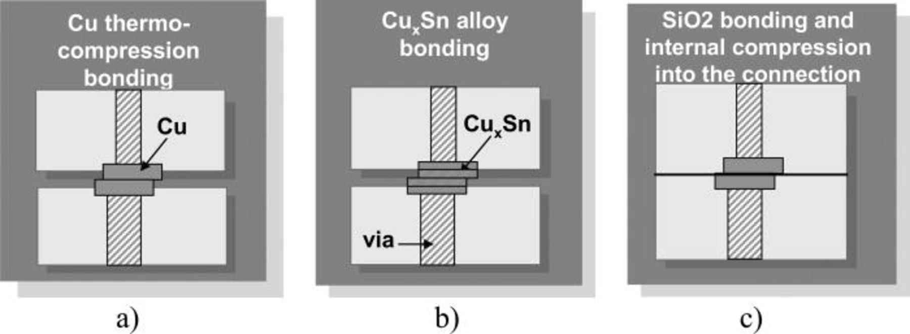
Figure 1. Different bonding schemes used for thermocompression technique: (a) Basic thermocompression (with or without glue between the pads), the temperature is around 400°C, (b) Same process but copper-tin alloy is used to decrease the temperature of the process to 250/300°C (c) Hybrid bonding; The compression in the metal pad is induced by the temperature and the high strength of the oxide/oxide bonding part (Ref. 17 ).
Bonding without a compression force: Direct bonding
Direct wafer bonding refers to a process by which two mirror-polished wafers are put into contact and held together at room temperature by adhesive forces, without any additional materials. 18 This technology has become more and more attractive for microelectronic and micro technology applications because it presents many advantages (Fig. 2). In this method the surfaces heterogeneous or not are bonded at room temperature. Bonded in an aligner a submicronic alignment can be though easily achieved. 20 Depending on the surface preparation the bonding energy can be monitored with respect to the surfaces to be bonded; as an example bonding energy of 3.8 J/m2 are obtained on oxide bonding with a plasma preparation with post bonding anneal. 21
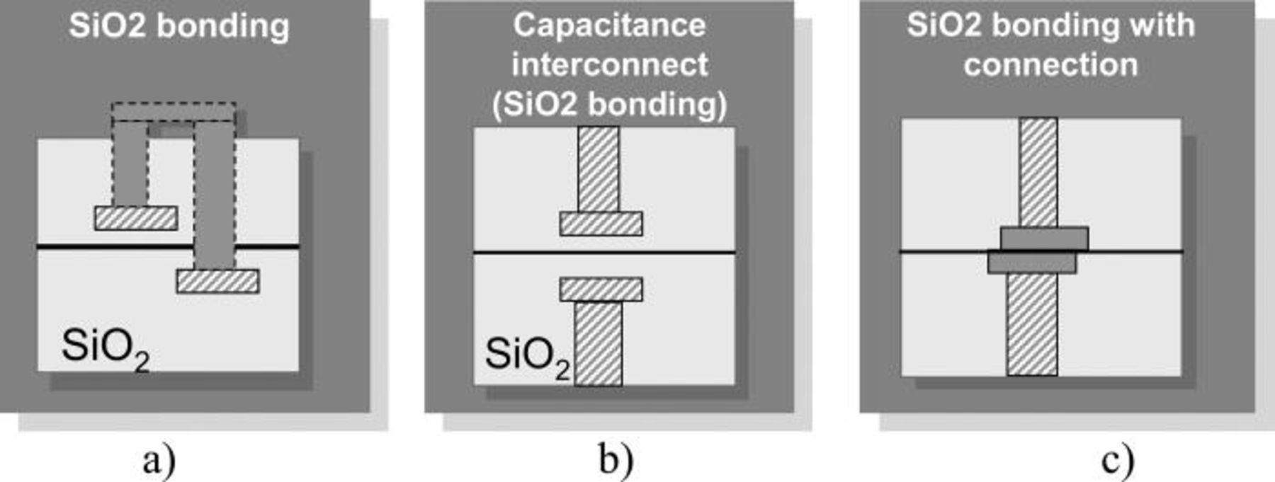
Figure 2. Different bonding schemes used for direct bonding techniques: (a) oxide bonding with precision alignment Two vias are necessary to contact the two layers (b) oxide bonding with alignment the contact is done via capacitance (Ref. 19 ) (c) direct bonding of hybrid oxide metal patterned surface.
For copper bonding ultra high vacuum (UHV) bonding has been investigated to avoid oxide formation. 22 Prior to bonding the Cu surface are activated in a UHV plasma with an Ar ion beam to remove the copper oxide. The bonding is then done at room temperature under high vacuum, a low temperature anneal around 200°C enhance the bonding strength. 23 Although high bonding energies (few joules per square meters) are demonstrated, the complexity of UHV tool as process trough put prevents this technology to be adapted in the industry.
Direct bonding of patterned oxide/copper surfaces at room temperature and ambient air was developed by the authors. This technique will be described in details in the next section of this publication.
Direct Copper Bonding Mechanism
Room temperature
To investigate the copper to copper direct bonding mechanism, the bonding interface at room temperature and its evolution with temperature was analyzed using complementary characterizations such as X-Ray Diffraction (XRD), X-Ray Reflectivity (XRR) and Transmission Electron Microscopy (TEM) characterizations. 10 nm TiN (CVD) and 1 μm of copper (200 nm PVD + 800 nm ECD) where deposited on oxidized 8-in. silicon wafers. CMP based surface preparation was used prior to bonding ensuring a low roughness and a high hydrophilic behavior of the copper surfaces. This surface preparation was described elsewhere. 24
TEM observations in Fig. 3 show a sharp interface at room temperature. At high magnification a 4 nm crystalline layer can be seen. This behavior is very different of standard bonding interface. Electron Energy Loss Spectroscopy (EELS) analyses have detected the presence of oxygen in this layer. With XRR measurements on stored samples a drop of electron density of about 4 nm width was recorded. The ratio of density at the interface ρ/ρCu value is in accordance with the ρCu2O/ρCu (Fig. 3). This layer is though the signature of the presence of a copper oxide at the interface. It can be assumed that this layer is created during the storage of the bonded wafers. XRR spectrum done just after bonding shows a more classical shape except the presence on each part of the interface of a shoulder underlying the presence of an oxygen enriched layer.
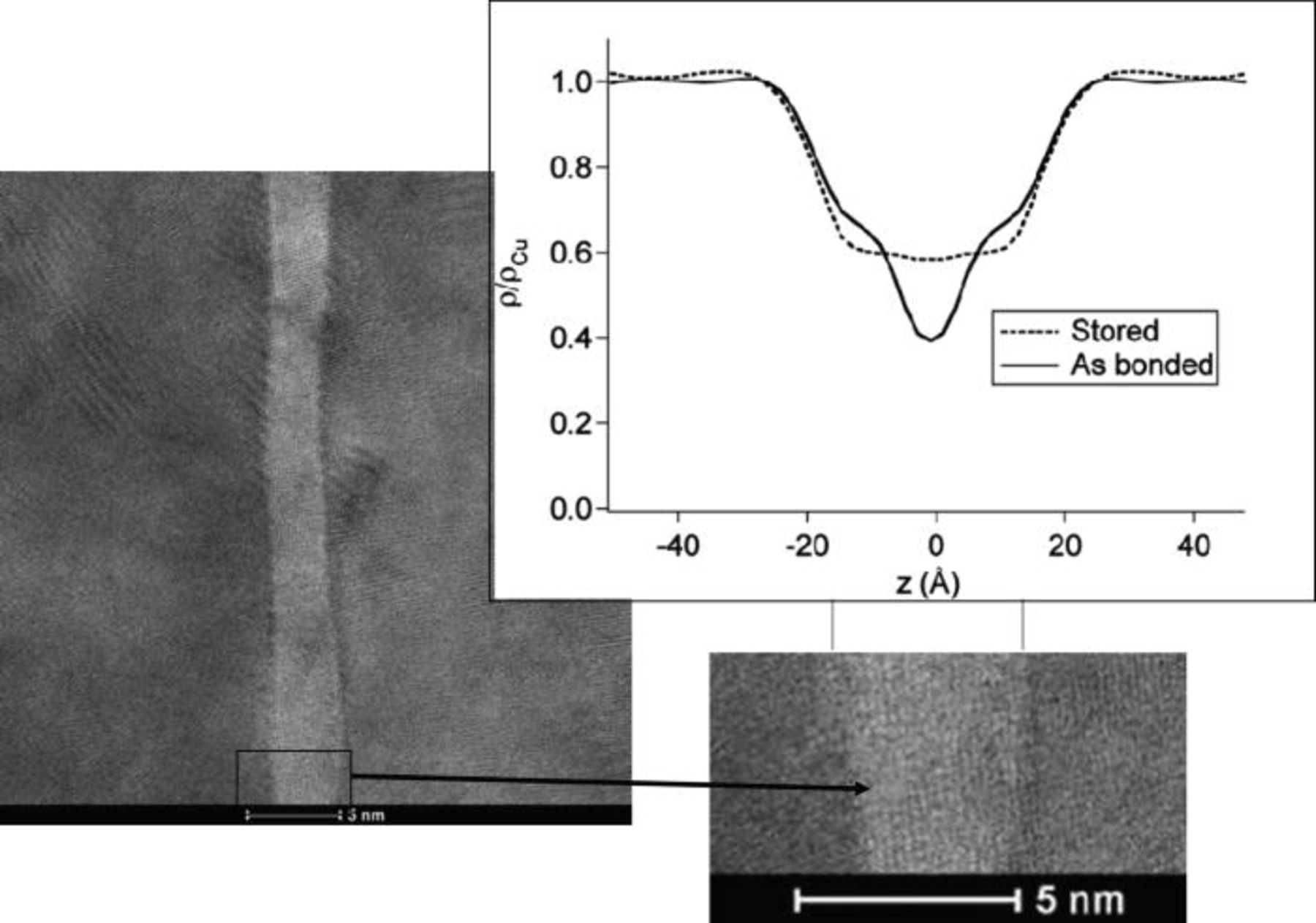
Figure 3. Transmission electron microscopy at high magnification of un-annealed copper bonded samples images the presence of a cristalline layer of 4 nm width. XRR measurments of electron density of as bonded and stored samples show the creation of this interfacial layer with time. The drop of electron density is about 4 nm width and the interface ρ/ρCu value is in accordance with ρCu2O/ρCu.
Evolution of the bonding toughness at room temperature as a function of the storage time was performed by Double Cantilever Beam (DCB) technique (Fig. 4). The increase of energy with storage time confirms the XRR and TEM observations. With time the bonding energy equals to standard bonding values at room temperature increases to 1 J/m2 after two days and ends to the bulk energy value after a few months storage. The bonded pairs are sealed just like they where epitaxied together.
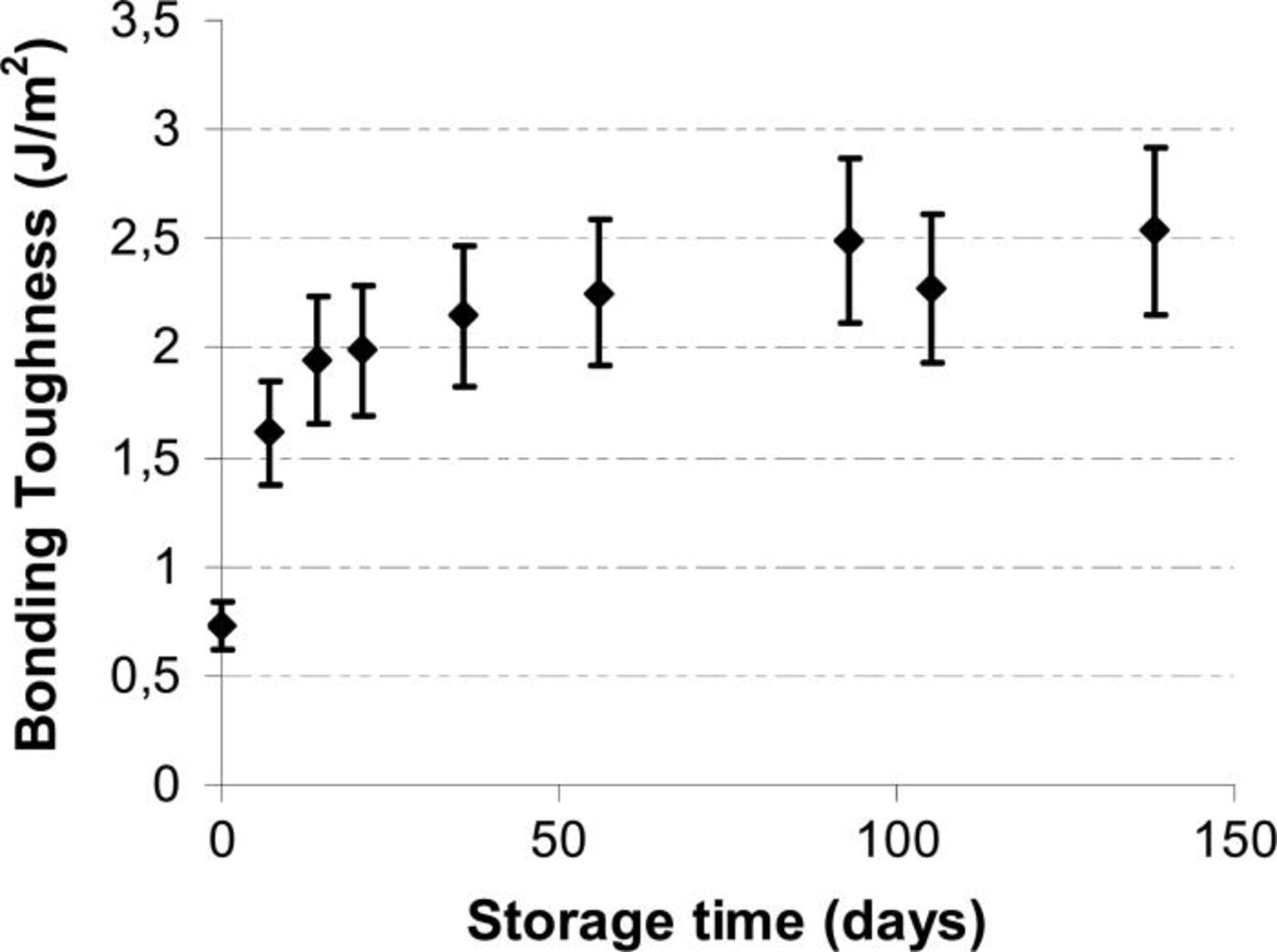
Figure 4. Room temperaure bonding toughness as a function of storage time.
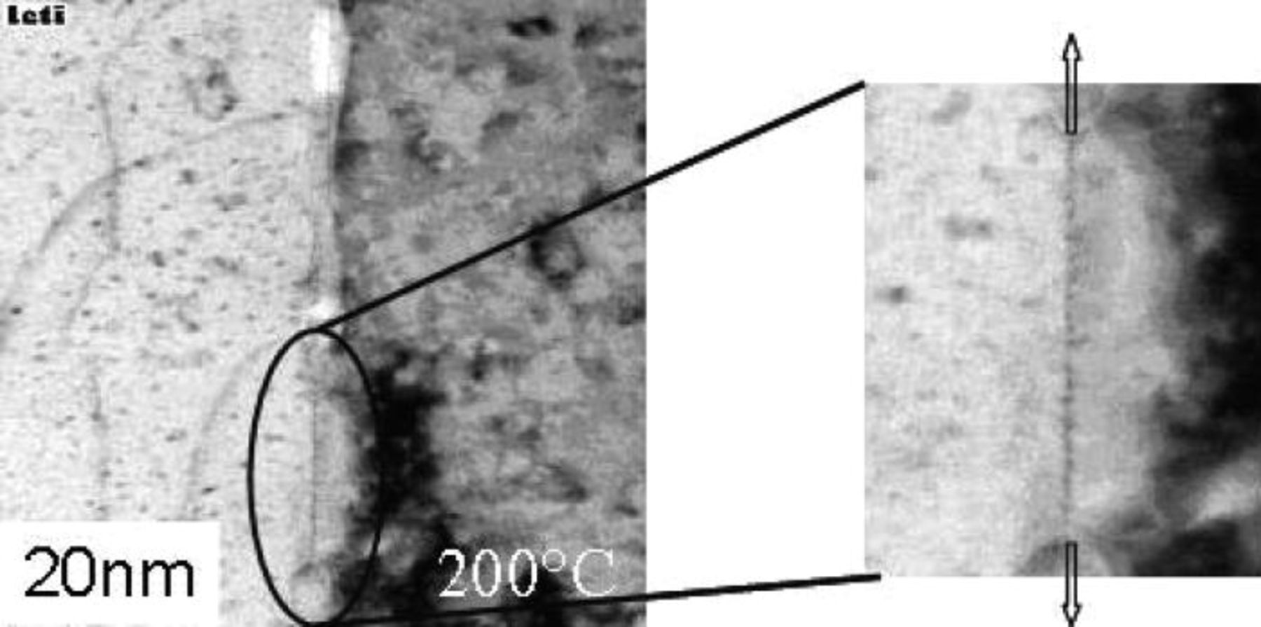
Figure 5. TEM cross section of a blanket Cu/Cu direct bonding after 200°C post bonding anneal for 30 min. The interfacial copper oxide diffuses along the bonding interface which allows intimate copper copper contact and creation of dislocations
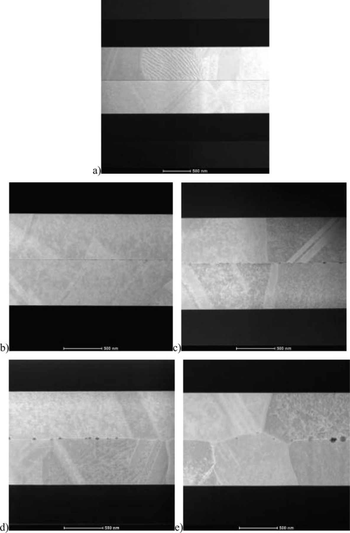
Figure 6. TEM cross section direct copper bonding interface evolution with successive 30 min. Post bonding anneal: RT (a), 100°C (b), 200°C (c), 300°C (d), and 400°C (e).
Behavior with temperature
At 200°C, the copper oxide becomes thermo dynamically instable, 25 its diffusion along the bonding interface is observed and diffusion bonding can happen. Nanovoids partially filled with oxide are created. A copper to copper grain boundary appears, and dislocations can be imaged at the bonding interface (Figs. 5 and 6). TEM and XRR measurements done in temperature confirm the sealing of the interface at 230°C.
This mechanism is similar to a diffusion bonding except that no pressure is applied. The diffusion bonding has been extensively studied in metal sintering 26 and consists in a plastic deformation of the asperities of both metal films. In our case we have a direct bonding at room temperature of highly hydrophilic surfaces. With temperature the strengthening of the interface is obtained by a diffusion like mechanism.
Patterned Copper/Oxide Bonding Mechanism
Due to a possible CMP non-homogeneity, the patterned surfaces might present different topologies within wafer or wafer to wafer. It is though mandatory that the bonding process is tolerant to those topologies (Fig. 7). This tolerance is obtained thanks to the dilatation of copper with temperature that enables the bonding even if the copper is in dishing. In case of copper in protrusion, this protrusion should be as small as possible to allow the oxide bonding.
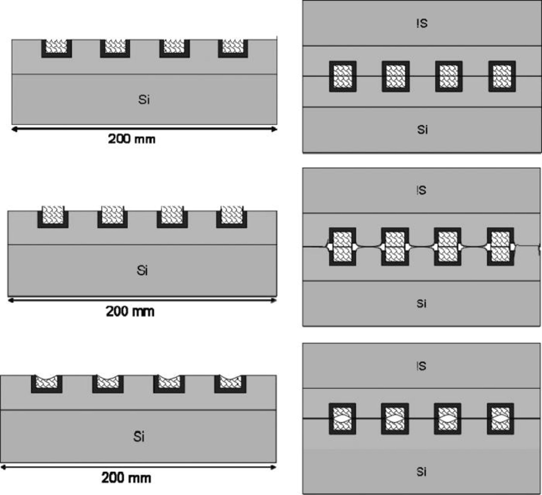
Figure 7. Schematic description of different surface topology possible on patterned surfaces: from up to bottom, flat surfaces, with copper in protusion and with copper in dishing. The resulting bonding is imaged in the right column.
Simulation of copper pad deformation with respect to temperature, pad size and height was done with Ansys software considering elastic properties of silicon and oxide and elasto-plastic properties of copper. It can be seen in Fig. 8 that the vertical displacement of the Cu pads varies with the pad geometry. Also the results show that a small dishing of copper pad will be overcome during the post bond annealing even at low temperature such as 200°C. It is also important to point out that the monitoring of the CMP step and the knowledge of the layout needed for a good bonding is mandatory.

Figure 8. Simulation of the vertical displacement of copper pads, as a function of pad geometry. H is the height of the copper line in micron.
Very good bonding and high bonding toughness can then be obtained with respect to this bonding behavior. Acoustic observations (SAM) do not show defects bigger than 30 μm (resolution of this equipment) (Fig. 10). Bonding toughness was recorded and ranged from 1 J/m2 at 200°C up to 6.6 J/m2 at 400°C confirming that the mechanism is identical to the described earlier (Fig. 9). Even at 200°C post bonding anneal it was possible to grind down to 5 μm the top silicon of the bonded pair.
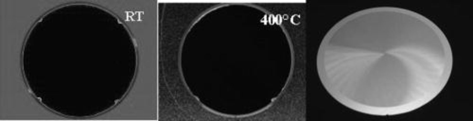
Figure 10. (Left) Acoustic image of bonded patterned wafers at room temperature, middle) same wafers after a 400°C anneal, (right) Picture of a bonded pair grinded down to 5 μm after a 200°C post bonding anneal.
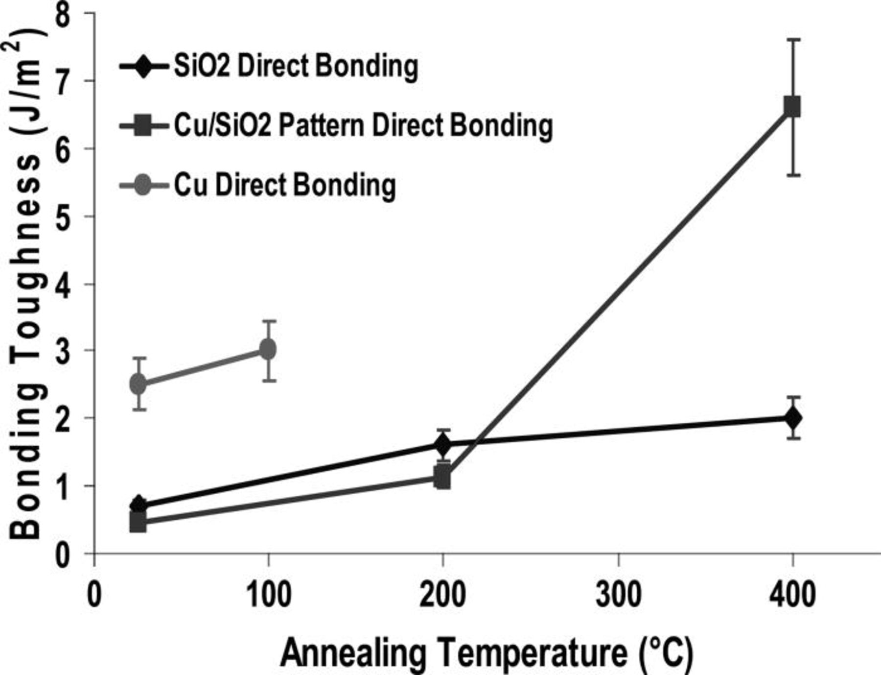
Figure 9. Bonding toughness with annealing temperature.
Alignment
To recover vertical interconnect in 3D technology, bonding with precision alignment is mandatory. As direct bonding is done at room temperature it maximizes throughput and eliminates contribution of wafer thermal expansion on misalignment. Therefore, the added stress to the bonded wafers impairing devices and interconnects and inducing wafer deformation are diminished or avoided. Reducing process-induced distortion is also key parameter to avoid a decrease in yield or reliability as well to improve critical alignment accuracy.
Face to face alignment between bonded wafers was performed in a EVG tool and was measured by means of a transmission IR microscope after bonding. The misalignment was measured on a micrometric vernier in five locations all around the wafer (one at center and four at edges: N, S, W, E). The used vernier allowed an accuracy of measurement below 0.1 μm. The results are given, in μm, in Fig. 11.
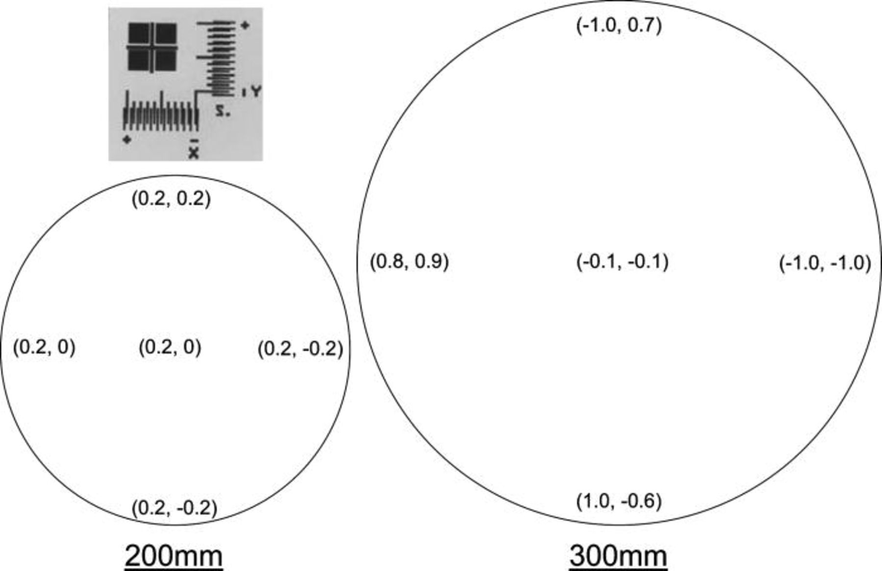
Figure 11. 200 m and 300 mm mapping for (x,y) misalignment given in μm. A vernier with the positive and negative direction for x and y is shown top left of the figure.
Based on further process optimization (e.g., planarization, surface treatments, etc) alignment of less than 1 μm across the wafer has been achieved using standard alignment marks and EVG Smart View® system. For 200 mm wafers, alignment below 0.2 μm is shown all around the wafer. For the 300 mm wafer pair, misalignment is below 1.0 μm at edge. As reported in literature, 27 the misalignment is a combination of an offset and a rotation between the bonded wafers and of an additional effect called run-out. The misalignment shift for both 200 and 300 mm wafer pairs is below 0.2 μm (respectively (0.2,0.0) and (0.1,0.0)). It demonstrates that the alignment control during bonding is accurate enough to ensure good alignment. As no external force or pressure is applied during wafer preparation and direct bonding process, we obtain a minimum mechanical deformation. Thus, the wafer to wafer direct bonding process leads to excellent alignment while ensuring a very high throughput.
Characterization of Direct Bonded Wafers: Acoustic Microscopy
To study the evolution of bonded structures with temperature, we have used wafers with different copper line widths. To image acoustic resolution and bonding behavior with temperature, it was chosen to bond pattern wafers on blanket oxide surface with copper features in small dishing. Then these 200 mm wafers have been annealed successively at 100, 200, 300, and 400°C for 2 h.
After the wafer bonding and successive annealing, the bonding interface quality is observed using an acoustic microscope. With a 110 MHz transducer, the effective lateral resolution is 7 μm and defects as thin as 5 nm can be detected in the Z-direction.
The Fig. 12 shows the evolution with temperature of a SAM signal on a set of half Kelvin crosses of sizes ranging from 15 to 25 μm. At room temperature, no copper areas are closed because of the residual CMP dishing: the whole features appear bright white. With temperature increase, the copper structures expand, filling the gap left by the CMP topology. When the copper surface comes into contact with the facing oxide surface, bonding occurs and SAM contrast disappears. In the smaller patterns, where the initial post CMP dishing is limited, the closing of the copper interface occurs at lower temperature (evolution is already visible at 200°C for the smallest crosses). In larger patterns, with higher dishing values, high temperature anneals are required to completely seal the bonding interface. It can be seen, Fig. 12, that all Cu features are completely bonded upon 400°C annealing.
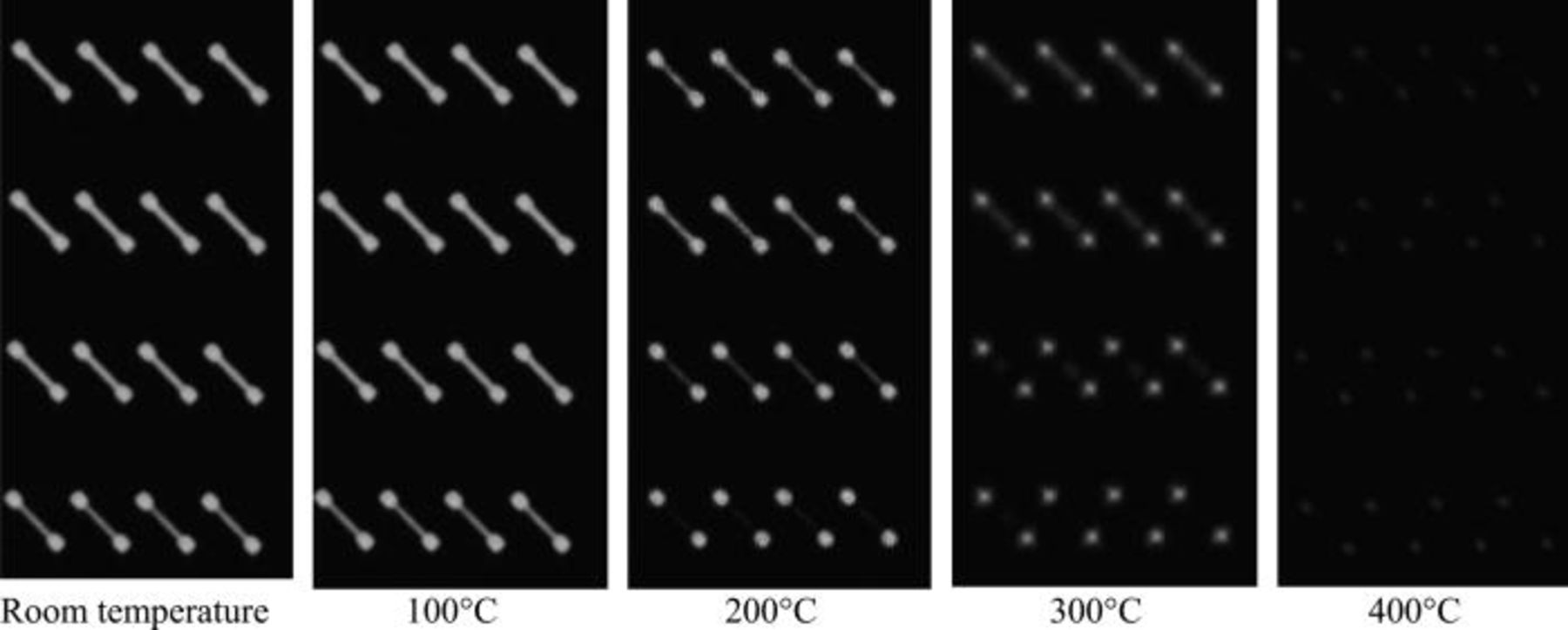
Figure 12. SAM evolution of half Kelvin crosses patterns with temperature, the width of the branch is respectively from top to bottom 25, 25, 20, and 15 μm.
This experiment demonstrates that this characterization technique can be successfully used to adapt the pre and post bonding process conditions with respect to the layout.
Characterization of Direct Bonded Wafers: Electrical Behavior of Daisy Chains
Daisy chains (DC) were used to investigate the electrical behavior of bonded structures. Different dimensions (contact area of 3 × 3 or 5 × 5 μm2) and various numbers of connections (5000 to around 30,000 connections) are tested.
The followed integration process was used to realize the electrical characterization: after bonding, the top silicon wafer is first removed down to the oxide using a combination of mechanical and chemical (TMAH) etching. The silicon oxide is finally dry etched down to bonding interface to enable probes to connect the copper pads (Fig. 13).
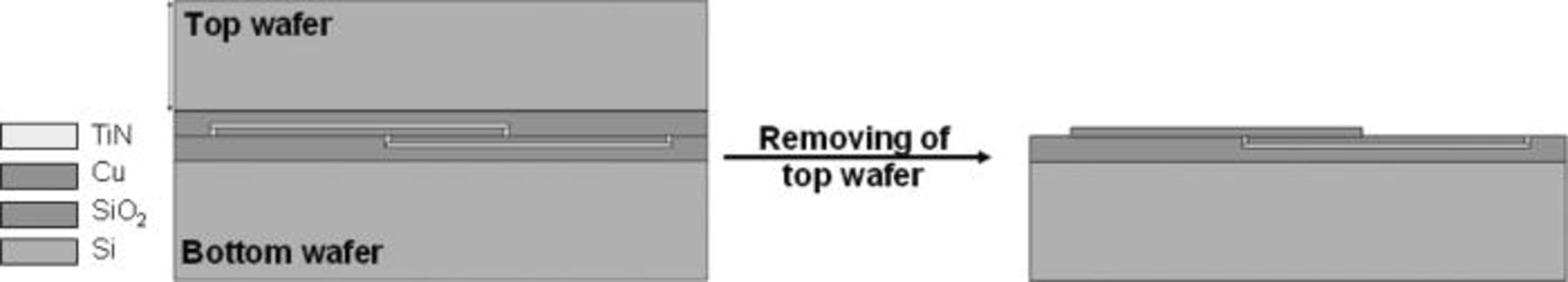
Figure 13. Bonded wafers after the complete removal of one silicon wafer and the SiO2 layer.
Figure 14 represents an optical picture of the bonded structure after the removal of the top wafer down to the bonding interface. The measured misalignment all over the wafer is less than 1 μm, and allows the connection between all the copper lines even in the highest density (3 × 3 μm2 contact area with a pitch of 14 μm on x-axis and 7 μm on y-axis).
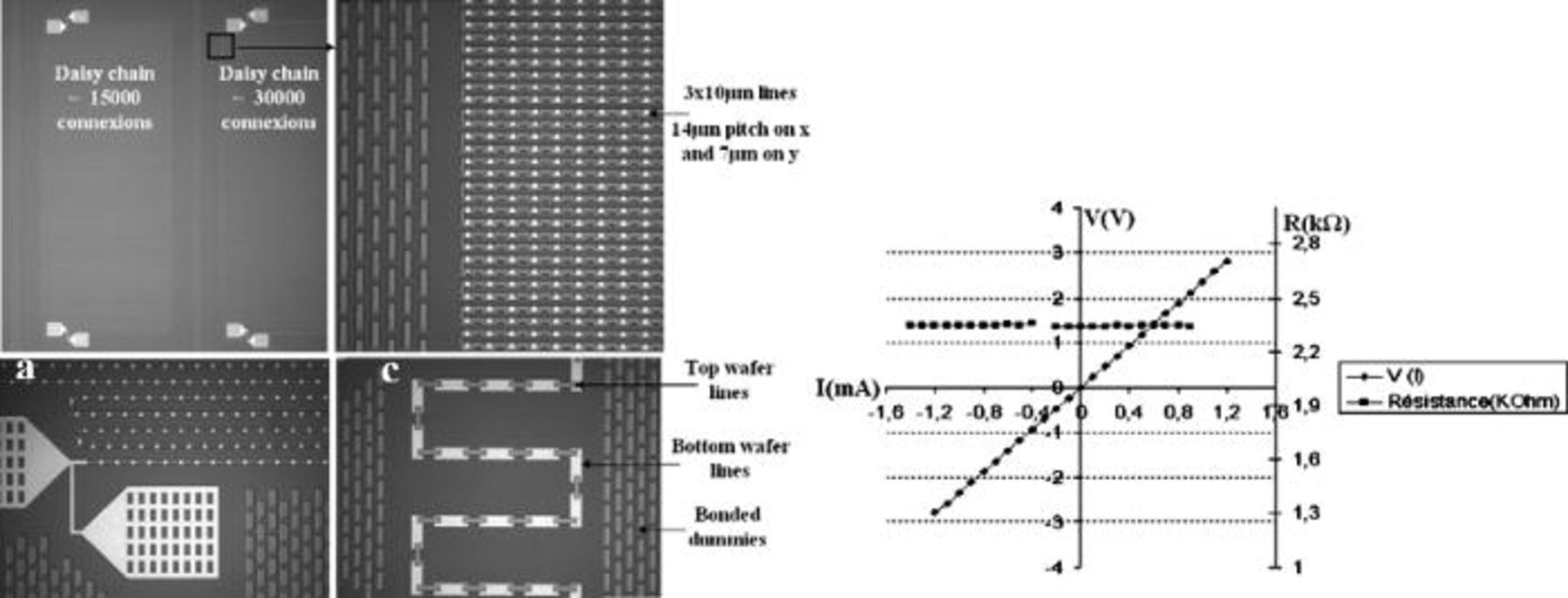
Figure 14. (Left) Optical observation of DC after the complete removal of top silicon wafer (right) V(I) and R(I) curves on a daisy chain of 29,422 connections with 3 × 3 μm2 contact area.
V(I) and R(I) characterizations for a daisy chain, with 29 422connections and a contact area of 3 × 3 μm2, after a 400°C anneal is presented in
Figure 14, a perfect ohmic behavior is observed for all the tested structures. Considering the chip size of 2 mm2, the density of interconnections for this daisy chain is estimated around d = 1.5 × 10⁶/cm2.
A total chain resistance of 2.34 kΩ is measured for this daisy chain, which corresponds to a resistance of 79.5 mΩ per node (node = bonding interface + Cu lines) (Fig. 15).
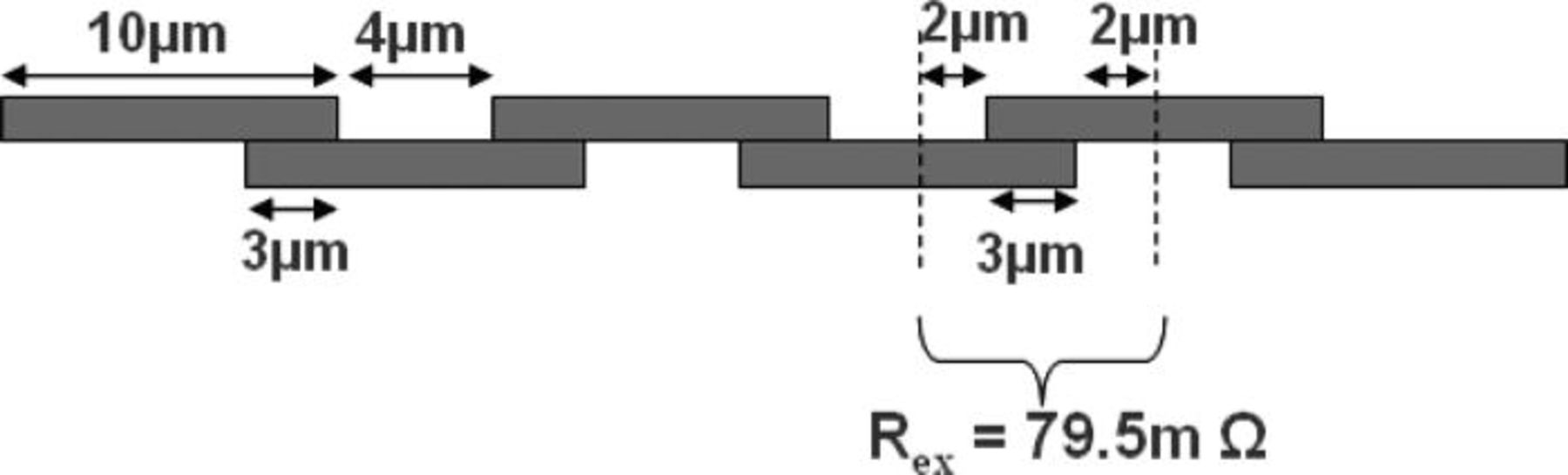
Figure 15. Representation of the experimental measurement of the resistance per node on daisy chain with 3 × 3 μm2 contact area.
Comparing the experimental with the theoretical calculation of the resistance per node (that leads to a value of 77 mΩ), a difference of 2.5 mΩ is obtained 28

This difference is induced by copper line resistance variations, ± misalignment error during bonding (impacting mainly the contact area) and the real bonding interface resistance Rc. In the worst case, where this difference is induced only by the bonding interface resistance, the estimate specific contact resistance (ρc) is
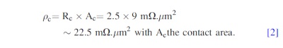
The specific contact resistance for a 400°C post bonding anneal is then around 22.5 mΩ μm2. These values of resistance and specific resistance show that there is an insignificant impact of the bonding interface. And that the bonded structures have almost the same electrical behavior than copper line bulk without interface. 28
For 200°C annealed structure, the extraction of the bonding interface resistance was achieved on daisy chain with 5 × 5 μm2 contact area. With the same assumptions than before, the bonded contact resistance is of Rc = 5.6 mΩ. This resistance leads to a specific contact resistance of ρc = 140 mΩ μm2.
The resistance obtained for the 200°C post bonding annealed sample is higher than the 400°C annealed, but this value is still very small and shows that for a 200°C post bonding anneal, there is no impact of the bonding interface on the electrical behavior.
Matching
In order to demonstrate the reproducibility of the electrical data at the wafer level, statistical measurements have been performed on more than 200 chips across the wafer area (200 mm wafer).
Figure 16 represents the distribution on more than 200 tested chips of the measured resistance of 29 422 interconnect daisy chain all over the wafer (3 × 3 μm2 contact area.). The yield is 88.5%. Table I describes the minimum, the maximum and the average value of the global resistance of the daisy chain. It shows also a small standard deviation σ = 1.18% that confirms the reproducibility of the bonding process all over the wafer.
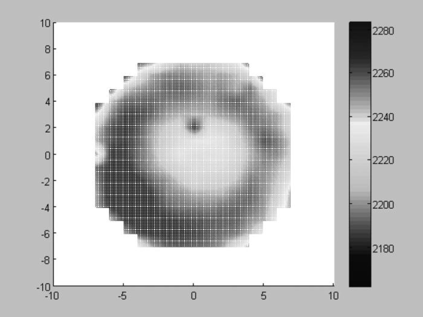
Figure 16. Wafer map of the 29,422 daisy chain resistance.
Table I. Electrical measurement of 30 000 interconnect daisy chains on 400°C annealed bonded wafer.
| Post bonding annealing | Min(Ω) | Max(Ω) | Average resistance(Ω) DC5 | Standard deviation(%) |
|---|---|---|---|---|
| 400°C for 2 h | 2162 | 2291 | 2202 | 1.18 |
Conclusion
For More Moore and More than Moore applications, low temperature bonding and metal bonding are becoming the main integration paths for 3D stacking. Thermocompression and direct bonding are the main researches pursued. We have presented our developments on direct Cu/Cu bonding at room temperature, atmospheric pressure and ambient air. A bonding mechanism is proposed to explain copper direct bonding on blanket and patterned wafers based on interface reconstruction. Evolution of the bonding interface to a grain boundary above 200°C was presented by coupling XRD, XRR and TEM analysis. Validation of copper direct bonding electrical contact was demonstrated on 29,422 interconnects daisy chains. Specific contact resistance of 22.5 mΩ μm was obtained for 3 × 3 μm2 contact areas. The contact resistance of a 3 × 3 μm2 contact resistance, 2.5 mΩ is negligible compared to the resistance of a via of 3 × 3 μm2 which is around 130 mΩ.
Centre d'Energie Atomique assisted in meeting the publication costs of this article.