
Abstract
Quantum dots have attracted considerable interest in the fields of solid state lighting, displays, and fluorescent imaging. Their tunable optical properties by changing the size and solution processability lead to commercial applications. In this review, we focus on the advancement of white light emitting nanocrystals, their usage as the emissive layer in LEDs and display backlights, and examine the increased efficiency and longevity of quantum dots based colored LEDs. In addition, we also explore recent discoveries on quantum dots as biological labels, dynamic trackers, and applications in drug delivery.
Export citation and abstract BibTeX RIS
Colloidal quantum dots are one of the most visually compelling examples of how materials can behave differently at the nanoscale. Using solution chemistry, one can grow crystals of a semiconductor in the reaction flask. In early growth, when the crystals are below 10 nm in diameter, the bandgap of these semiconductor nanocrystals is size dependent, allowing for simple tuning of their absorption and emission spectra. Louis Brus was the first to show that when the radius of the crystal is below the bulk Bohr exciton radius, confinement energy of the exciton modifies the bandgap energy.1 Murray et al. would later publish a seminal paper describing the synthesis of monodisperse CdSe nanocrystals.2 The incredible power to tune a single material's optical properties simply by size in addition to the added advantages of solution processability indicated early on that colloidal quantum dots could have commercial applications in lighting and display technology. However, as synthesized, the efficiency of the light emitted is very low. In this review article, we will discuss emissive quantum dots and their uses in solid state lighting, displays, and biological applications.
Emissive Quantum Dots
Core shells
The primary roadblock toward immediate commercial application was that the as-synthesized nanocrystals were not efficient nor photostable enough to begin to compete with contemporary lighting and display technologies. The semiconductor industry has long been aware of the technical challenges surfaces can create. Compared to thin film devices, colloidal nanocrystals are dominated by surfaces. Specifically, the surface of a nanocrystal is composed of cations predominantly passivated by the surfactants used in the synthesis, while the anions remain mostly unpassivated and subject to oxidation. The dangling bonds as a result of under-coordinated surface atoms act as charge traps for photogenerated carriers, lowering the fluorescence efficiency.
To eliminate these surface traps, Hines et al. developed a method of growing a shell of a wider bandgap material (Figure 1).3 These early core/shell quantum dots demonstrated a dramatic increase in fluorescence efficiency, which was on the order of 30%, and improved photostability. A start-up company (Quantum Dot Corp.) would use these crude core/shell quantum dots as a starting point for what would be the first major commercial product based on colloidal quantum dots. Their goal was to build technology platforms based on stable and bright fluorescence. This could evolve to the use of QDs as probes for biological imaging. Compared to conventional fluorescent dyes, the quantum dots exhibit superior brightness and far narrower emission spectrum. Further, the continuum absorption of the quantum dots could enable multi-color imaging with the need for only one excitation wavelength.

Figure 1. TEM image of CdSe/ZnS nanocrystals. Reprinted with permission from Ref. 3. Copyright 1996 American Chemical Society.
At the time of the initial start-up, little was known about the nature of the inorganic shell and there were very few protocols for transferring quantum dots from non-polar to aqueous, bio-friendly solutions. In order to develop improved shell coverage, advanced electron microscopy in conjunction with Rutherford backscattering spectroscopy was employed to gain unprecedented look into the true shell coverage. Through collaboration with Stephen Pennycook, atomic number contrast scanning transmission electron microscopy, or Z-STEM, was utilized to obtain the first true images of the shell coverage.4,5
Unlike convention HRTEM, the intensity of the electrons collected by a high angle annular dark field detector (HAADF) is dependent on the atomic number of the scattering atom.6 This elegant mode of 'what you see is what you get' imaging showed in great detail how the shell deviated strongly from the perfectly uniform coating oft depicted in cartoons. As shown in Figure 2, the shell clearly growing off of one surface, leaving the other surfaces of the core with minimal or no passivation. The result of this shell motif is an improved quantum yield but continued susceptibility to quenching and photobleaching.
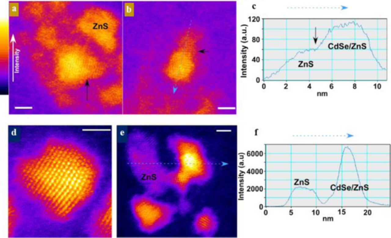
Figure 2. Z-STEM of early CdSe/ZnS quantum dots showing asymmetric shell growth. Reprinted with permission from Ref. 4. Copyright 2006 American Chemical Society.
There were two possible reasons why the shell preferred to grow off of one surface. Since the CdSe cores had a wurtzite crystal structure, not all surfaces are chemically equivalent, yielding surfaces that can be cation or anion rich.7,8 In particular, the Se-rich surfaces are relatively un-passivated by ligands. This increases their reactivity resulting in accelerated shell growth. Later, with the atomic resolution afforded by aberration-correction, the shell growth would unambiguously be shown to favor the anion rich surfaces. To a lesser extent, lattice mismatch between CdSe and ZnS may also contribute to the anisotropic growth. After a monolayer of ZnS is grown on a surface, the shell material can relax creating a defect at the interface, allowing for latticed-matched shell growth.
With a clear picture and mechanistic understanding of the anisotropic shell growth, shells of CdS were chosen instead of ZnS. Aberration-corrected Z-STEM images shown in Figure 3 indicate that although the shell coverage is still preferentially covering the anion-rich surfaces yielding a bullet-shape particle, enough shell is grown to cover all the surfaces.
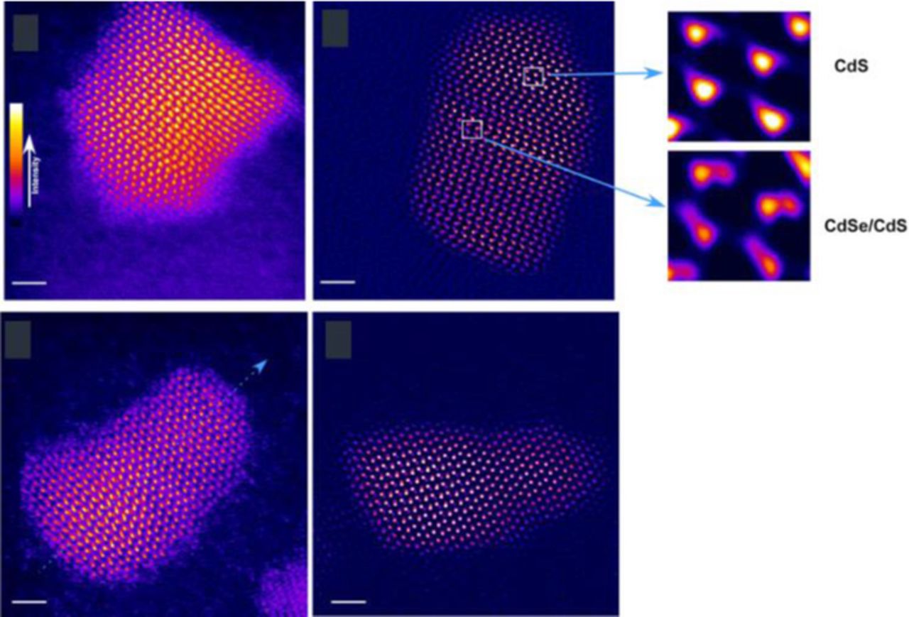
Figure 3. Aberration-corrected Z-STEM of QD655s showing the 'nanobullet' morphology. Reprinted with permission from Ref. 4. Copyright 2006 American Chemical Society.
With the addition of amphiphilic polymer 'shell', the quantum yield of this material approached unity in water. Currently, CdS is still the shell material of choice for CdSe and other core materials. Through successive ion layer addition and reaction (SILAR) processes, shells of CdS can be grown upwards to 20 monolayers.9 These 'giant shelled' quantum dots exhibit extreme photostability as the core is believed to be completely isolated from the surface.10
White light-emitting nanocrystals
The most common sources of lighting today are incandescent and fluorescent bulbs. These sources of light only have efficiencies of about 5 and 25%, respectively. In both designs, most of the energy lost is due to the release of heat. Solid state lighting releases very little heat, requiring less energy to produce the same amount of light. A pure white light LED is needed to replace the traditional lighting.11 Previous methods of producing white light LEDs have utilized a blue LED with a yellow fluorescent phosphor or combining red, green, and blue emitting nanocrystals. The yellow phosphors require rare earth elements and have a low color quality and a halo effect due to scattering. When using multiple sizes of nanocrystals to create the red, green, and blue emission, the emission intensity is decreased due to self-absorption.
First attempts to synthesize white light emitting nanocrystals included the combination of band edge emission with conventional deep trap states of ZnSe quantum dots.12 In 2005, Bowers et al. synthesized ultrasmall CdSe nanocrystals, via a pyrolytic method, that emit a broad spectrum of light from 420 to 710 nm.13 These nanocrystals do not suffer from self-absorption due to their large Stokes shift of 40–50 nm. This broad emission has three unique features.14 The first peak at 440 nm is pinned at diameters less than 1.7 nm because of an energy state mediated by the alkyl phosphonic acid surface ligand. The second peak at 480 nm has an unknown origin, but it is believed to be due to residual tributylphosphine coordinated to the surface. The third broad peak at 560 nm is due to conventional deep trap emission believed to be associated with surface Se dangling bonds. With the high surface-to-volume ratio, the intensity of the third peak is equal to that of the blue and green peaks (Figure 4). This discovery stimulated a tremendous amount of research to improve and provide alternates for solid state lighting.
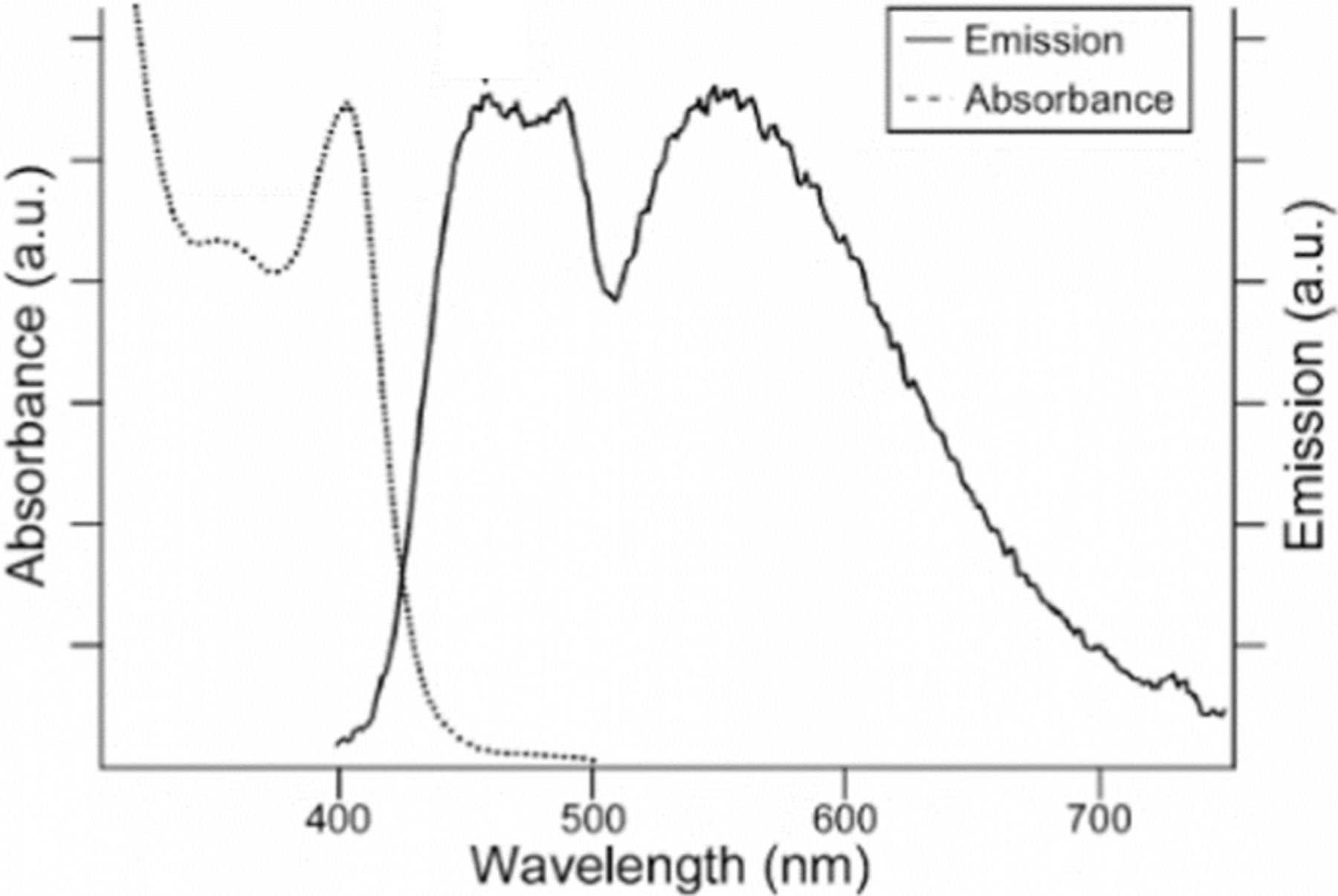
Figure 4. Absorption and emission spectra of ultrasmall CdSe. (λex 367 nm). Reprinted with permission from Ref. 13. Copyright 2005 American Chemical Society.
Although this leads to a balanced white light with CIE (Commission Internationale de L'Eclairage, 1931) coordinates of (0.32, 0.37), these nanocrystals suffered from a low quantum yield of 10%. Rosson et al. brightened the ultrasmall CdSe nanocrystals by performing a post-synthesis treatment with formic acid.15 This treatment increased the quantum yield up to 45% (Figure 5). The formic acid ligand partially exchanges with the phosphonic acid ligand, while also passivating previously non-radiative trap states. With this increase in quantum yield, the CIE coordinates also change to a bluer emission of (0.24, 0.24).

Figure 5. Absorbance (dashed) and emission (solid) of original (blue) and formic acid treated (red) CdSe nanocrystals. Inset: Vials containing concentrated white-light CdSe nanocrystal solutions before (left) and after (right) a sample formic acid treatment. Reprinted with permission from Ref. 15. Copyright 2012 American Chemical Society.
Recently, Dolai et al. reported ultrasmall, white light-emitting CdSe nanocrystals synthesized via a low temperature method.16 This is possible due to the highly reactive, phosphine-free Se precursor. This reaction produces a broad emission consisting of a sharp band edge emission and a broad trap state emission from various surface defects. The CdSe nanocrystals were synthesized with either oleylamine (CdSe-OLA) or both oleylamine and benzoic acid (CdSe-OLA/BA). The CdSe-OLA displayed CIE coordinates of (0.31, 0.32) and a QY of 11.2%. The CIE coordinates values shifted to (0.33, 0.34) and the quantum yield increased 26.9% when CdSe was synthesized with OLA and BA (Figure 6). When semiconductor nanocrystals are synthesized in the presence of anionic ligand, such as benzoic acid, the surfaces are found to be metal rich. This Cd(O2CPh)2 is bound to the surface Se sites, whereas the OLA is bound to the surface Cd sites. This passivation of both the surface Cd and Se prevents the formation of charge trapping sites, leading to the increase in the QY.
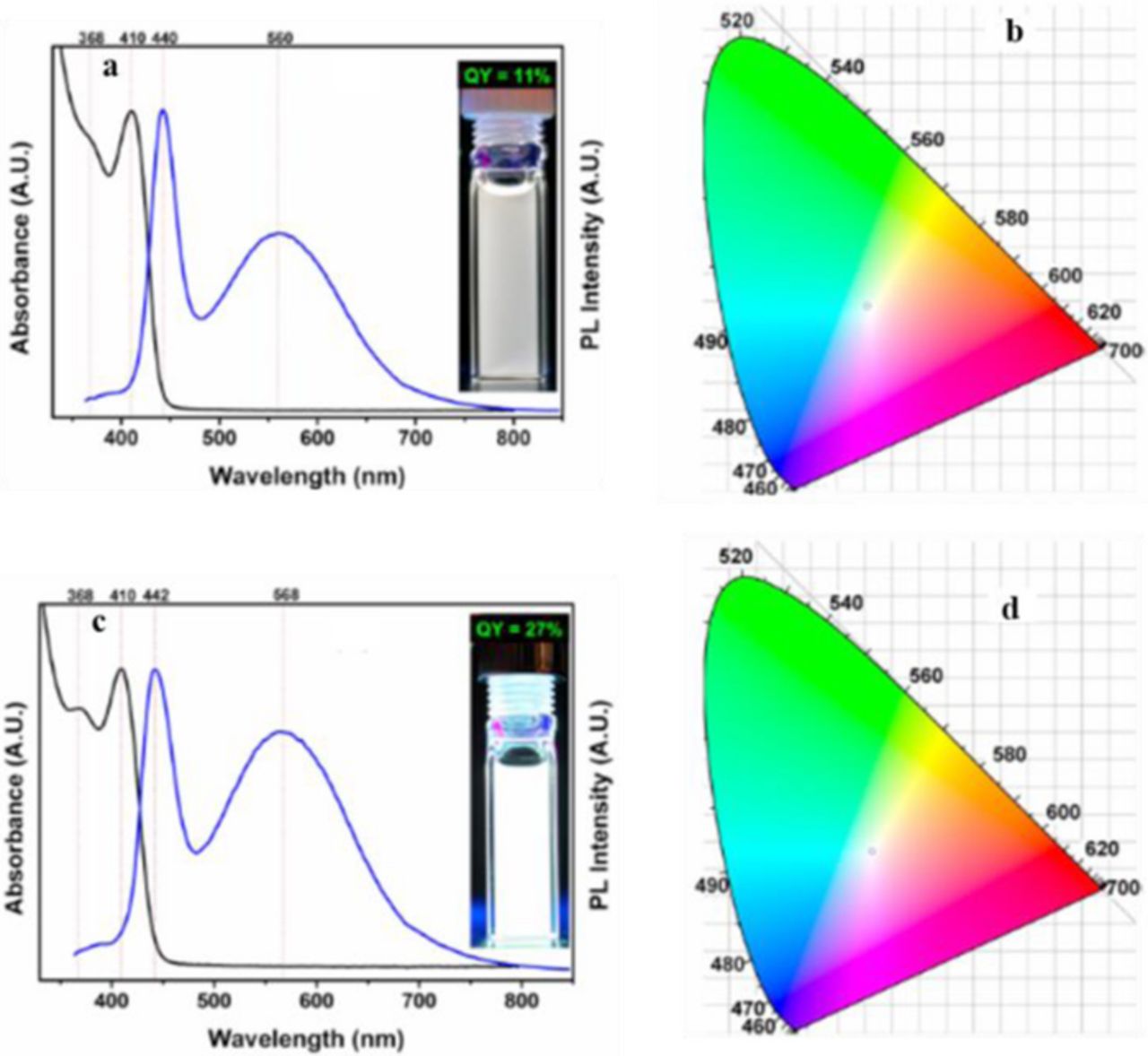
Figure 6. (a) UV−vis absorption (black) and PL (blue) of CdSe(OLA) nanocrystals. (b) CIE coordinates (0.310, 0.316) of CdSe(OLA) nanocrystals. (c) UV−vis absorption (black) and PL (blue) of CdSe(BA/OLA) nanocrystals. (d) CIE coordinates (0.330, 0.337) of CdSe(BA/OLA) nanocrystals. Reprinted with permission from Ref. 16. Copyright 2015 American Chemical Society.
Another method of generating white light emitting nanocrystals is by doping. This was first done in 2007 by Nag et al. by combining the surface state emission of CdS nanocrystals (broad peak, ∼500 nm) with the inner core transition, 4T1-6A1, emission of doped Mn2+ (620 nm).17 The emission is extended to longer wavelengths compared to conventional trap states because of the dopant. The advantage of using a dopant material, such as Mn2+, is the decreased sensitivity of the chromaticity due to particle size and distribution. With a dopant, the emission color is not dependent on the bandgap emission, but on the ratio between the surface state and dopant emission. Since the intensity of the emission at 620 nm can be tuned by changing the Mn2+ concentration, the shade of white light can be altered. When the CdS nanocrystals with an average particle size of 1.8 nm were doped with 0.10% and 0.19% Mn2+, the CIE chromaticity coordinates were (0.30, 0.40) and (0.35, 0.40), respectively (Figure 7). As the Mn2+ concentration increased, the peak at 620 nm increased, generating a more yellow emission. Although the tunability of white light is advantageous, these doped particles only have a measured quantum yield of about 2%.
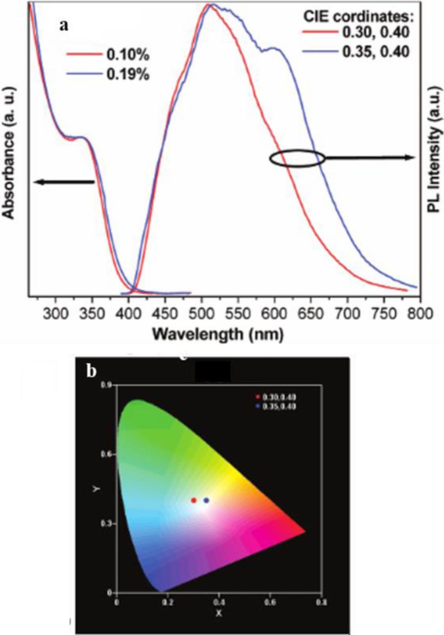
Figure 7. (a) UV-visible absorption and PL spectra of 0.10 and 0.19% Mn2+-doped CdS NCs. (b) CIE diagram showing the chromaticity coordinates of the produced white light of different shades corresponding to the PL spectra of (a). Reprinted with permission from Ref. 17. Copyright 2007 American Chemical Society.
To avoid using toxic materials, such as cadmium, Sharma et al. reported tunable white-light emission from Mn-doped ZnSe nanocrystals.18 This white-light emission originates from three emission states. The first, at 410 and 435 nm, is from the MnSe cores; the second, at 520 nm, from Zn-vacancy related defect states; and the third, at 580 nm, from the Mn-dopant. Once again, the emission can be tuned to emit different shades of white, in this case by varying the excitation wavelength from 325 to 400 nm (Figure 8). Spherical MnSe cores are first synthesized (2 and 4 nm diameters), followed by three Zn injections. As the number of Zn injections increased, the shaped turned from spherical to branched with a core size of 4.3 nm and branch length of 5.2 nm. With this deviation from a spherical to a branched shape, the PL intensity decreases. When excited at 300 nm, these nanocrystals have luminous efficacy up to 401 lm/W, and CIE coordinates of (0.34, 0.46). As the excitation wavelength is increased, the luminous efficacy decreases, but the emission color shifts toward pure white light.
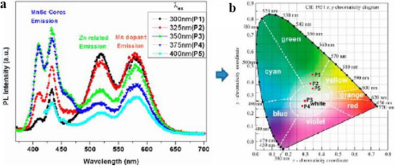
Figure 8. (a) PL spectra of the modified Mn-doped ZnSe NCs under excitation at various wavelengths. (b) CIE chromaticity diagram for Mn-doped ZnSe NCs. Reprinted with permission from Ref. 18. Copyright 2014 American Chemical Society.
An issue that has been found with previous methods of doping nanocrystals is their stability. Since there is a strong lattice mismatch between the nanocrystal lattice and the doping atoms, the dopants are found mainly on the surface. This leads to low luminescence intensity in aqueous environments. By doping with both Mn and Cu into separate layers, Wang, C. et al. was able to generate a stable aqueous white-light generator.19 Nanocrystals were synthesized by first preparing a Mn-doped ZnSe core, followed by a ZnS layer. CuCl2 was then injected to obtain a surface doped Mn:ZnSe/Cu:ZnS nanocrystal. To increase the stability of the nanocrystals, they were then enveloped with additional ZnS layers. The Mn:ZnSe emit at 480 and 585 nm, due to ZnSe trap states and Mn-dopant states, respectively. After the first layer of ZnS was synthesized, the PL intensity increased without a change in the peak wavelengths. The trap emission at 480 nm shifted to 477 nm after Cu doping. As the outer ZnS layers are added, the PL increases in intensity due to passivation of ZnSe surface defects. Also, as the number of ZnS layers are increased, the CIE coordinates shift from (0.29, 0.32) to (0.41, 0.38) (Figure 9). Values for quantum yield were not given.
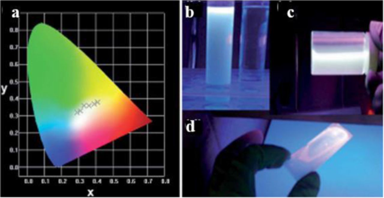
Figure 9. (a) (CIE) color coordinates of the Mn:ZnSe/Cu:ZnS QDs with different growth times of the ZnS layers outside the Cu impurities The corresponding CIE coordinates are (0.29, 0.32), (0.32, 0.36), (0.33, 0.32), (0.35, 0.36), (0.39, 0.37), and (0.41, 0.38). (b-d) Images of QDs under the irradiation of a 365 nm UV lamp (10 W). (b) Aqueous Mn:ZnSe/Cu:ZnS QD solution (left) and water (right). (c) Mixture of QDs and PVP aqueous solution. (D) Spin coating of the mixture in (c) on a glass slide. Reproduced from Ref. 19 with permission of The Royal Society of Chemistry.
Most recently, Pramanik et al. reported forming two different complexes with organic ligands on the surface of Mn:ZnS nanocrystals that display white light.20 The prepared Mn-ZnS nanocrystals were reacted with a mixture of hydroxyquinoline (HQ) and acetylsalicylic acid (ASA) to form MQ2 and M(ASA)2, where M = Zn and Mn. The M(ASA)2 emits at 410 nm, ZnQ2 at 500 nm, and Mn2+-dopant at 588 nm. The intensity of these peaks can be tuned by changing the concentration of the ligands (Figure 10). When reacted with a 1:1 molar ratio of HQ and ASA, the complexed Mn:ZnSe nanocrystals have a 2.2% QY and exhibit CIE coordinates of (0.30, 0.33) when excited at 320 nm. It was also found that as the excitation was changed, the chromaticity could be tuned. This complex is also photostable in the solid state, which will be useful in future light-emitting diodes.
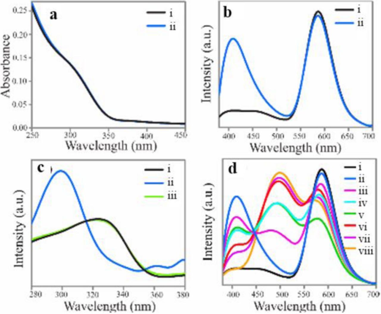
Figure 10. (a) UV−vis and (b) emission (λex = 320 nm) spectra of (i) ligand-free Mn2+-doped ZnS QDs and (ii) ASA-added Mn2+-doped ZnS QDs. (c) Excitation spectra of (i) ligand-free Mn2+-doped ZnS QDs at λem = 588 nm and (ii, iii) ASA-added Mn2+-doped ZnS QDs at λem = 410 and 588 nm, respectively. (d) Emission (λex = 320 nm) spectra of QDs following complexation with the mixture of 1.0 mM of ASA and HQ with ratio: (i) 0:0, (ii) 1:0, (iii) 4:1, (iv) 3:2, (v) 1:1 (vi) 2:3, (vii) 1:4, and (viii) 0:1. Reprinted with permission from Ref. 20. Copyright 2015 American Chemical Society.
Another more environmentally friendly method of generating white light from semiconductor nanoparticles is by using Group IV materials. Carbon containing nanoparticles have been used as a light emitting material since 2006. There are many facile methods of synthesizing carbon nanoparticles that are capable of controlling shape, size, and physical properties. Wang, F. et al. produced carbogenic (oxygen containing carbon) nanoparticles by thermal oxidation of citric acid in molten LiNO3, which serves as an oxidizing and basic media.21 The surface of these particles are passivated with poly(ethylene glycol) (PEG1500), which allows them to be dispersed in various solvents. When excited with blue light, the carbon nanocrystals have a broad emission that covers the entire visible spectrum. After passivation with PEG1500, the quantum yield increases from 3% to 10%. As the excitation wavelength is increased, the emission shifts to longer wavelengths. At an excitation wavelength of 407 nm, the carbon nanocrystals have CIE coordinates of (0.31, 0.32), almost pure white (0.33, 0.33). Mao et al. reported similar quantum yields (9.0%) with carbon dots synthesized by a one-step pyrolysis of poly(acrylic acid) (PAA) mixed with glycerol (Figure 11).22 The PAA is the carbon source, while the glycerol is used as the solvent and for surface passivation. Unlike the carbon nanocrystals passivated by PEG1500, these carbon nanocrystals have a more monodisperse sample, with an average size of 3.4 nm. These particles also show chromaticity tunability due to varying the excitation wavelength. The 9.0% quantum yield was obtained when excited at 347 nm and had CIE coordinates at (0.24, 0.29). After 30 h of UV irradiation it was found that the PL intensity does not decrease. Another extremely abundant and nontoxic Group IV material that has been used, but not widely developed as a white-light generator are silicon nanocrystals.
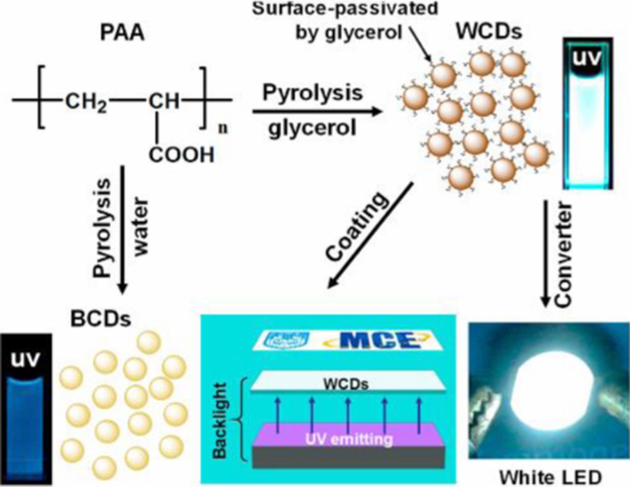
Figure 11. Illustration of the route for the synthesis of WCDs and their applications in backlight and white LED. Reprinted with permission from Ref. 22. Copyright 2014 American Chemical Society.
Lee et al. synthesized silicon nanocrystals from sodium silicide in organic solvents using ultrasonic energy and adding a SiCl4 modifier.23 After an hour of sonication, the nanocrystals emit from 340 to 700 nm (Figure 12). Neither quantum yield nor CIE coordinates were given for this experiment.

Figure 12. (a) Room temperature photoluminescence spectra of silicon colloids. The excitation wavelength used was 325 nm He–Cd laser. (b) The color photograph displays white as the sample is irradiated with the commercial low-intensity UV lamp (360 nm). Reproduced with permission from Ref. 23. Copyright 2004 Wiley InterScience.
Applications
Lighting
Colloidal quantum dots are ideal in the application as the emitting layer in light emitting diodes (LEDs) due to their tunable colors, bright emission, solution processability, and stability. The earliest experimental QD-LEDs were fabricated in the early 1990s and were comprised of a CdSe core or a core/shell QD –polymer bilayer or blend charge transport layer (CTLs).24 External quantum efficiencies (EQE) of up to 0.22% were reported. The low EQE is due to parasitic polymer electroluminescence. The next generation of QD-LEDs was introduced in 2002 by Coe et al.25 In this study, a monolayer of QDs is sandwiched between two organic small molecule thin film CTLs, recording a EQE of 0.5%. Anikeeva et al. fabricated QD-LEDs by microcontact printing the QD layer, which avoids exposing the organic charge transport layer to solvents.26 These devices reported a maximum EQE of 2.7% for orange emission. The third generation of QD-LEDs replaced both of the organic with inorganic charge transport layers. Inorganic CTLs are more stable to air compared to organic ones. This stability could lead to higher current densities. Examples of inorganic charge transport layers are sputtered metal oxide thin films. The energy band of these oxides can be fine-tuned due to the variety of compositions. Inorganic layers are also more conductive than the organic layers. Caruge, et al. applied this method using zinc tin oxide and NiO as the n- and p- type CTLs, respectively.27 The reported EWE was low at <0.1%, due to damage of the QD layer during the sputtering process. The fourth generation of QD-LEDs consists of hybrid organic and inorganic CTLs. Generally the n-type layer is a metal oxide which, in recent research, has been solution processed metal oxide nanoparticles. Since the QD layer is not damaged during fabrication, EQEs have greatly improved. A series of blue, green, and red QD-LEDs with external quantum efficiencies over 10%, have been reported by Yang et al. that are fabricated with an electron transport layer (ETL) of ZnO nanoparticles.28 They have achieved these efficiencies by tailoring the nanostructure and composition of the quantum dots. A graded alloy intermediate shell is inserted between the CdSe core and the ZnS outer shell to reduce Auger recombination. This recombination occurs when an electron and hole recombine and transfer the energy to an electron in the conduction band, which thermalizes back down to the valence band. ZnSe provides better confinement of the electron wavefunction compared to the commonly used outer shell material, CdS, due to the higher conduction band. Since thick shells of ZnSe and ZnS are not necessary to guarantee carrier confinement in the QD core, charge injection into the QD-LEDs is improved, leading to long device lifetime with a high efficiency. Green QD-LEDs fabricated with the ZnSe rich QDs had an external quantum efficiency and current efficiency (ηA) of 14.5% and 63 cd A−1, compared to that of 7.5% and 31 cd A−1 from CdS rich QDs. In addition, the blue and red QD-LEDs had EQEs of 10.7% and 12.0% and ηA of 4.4 and 15 cd A−1, respectively (Figure 13).
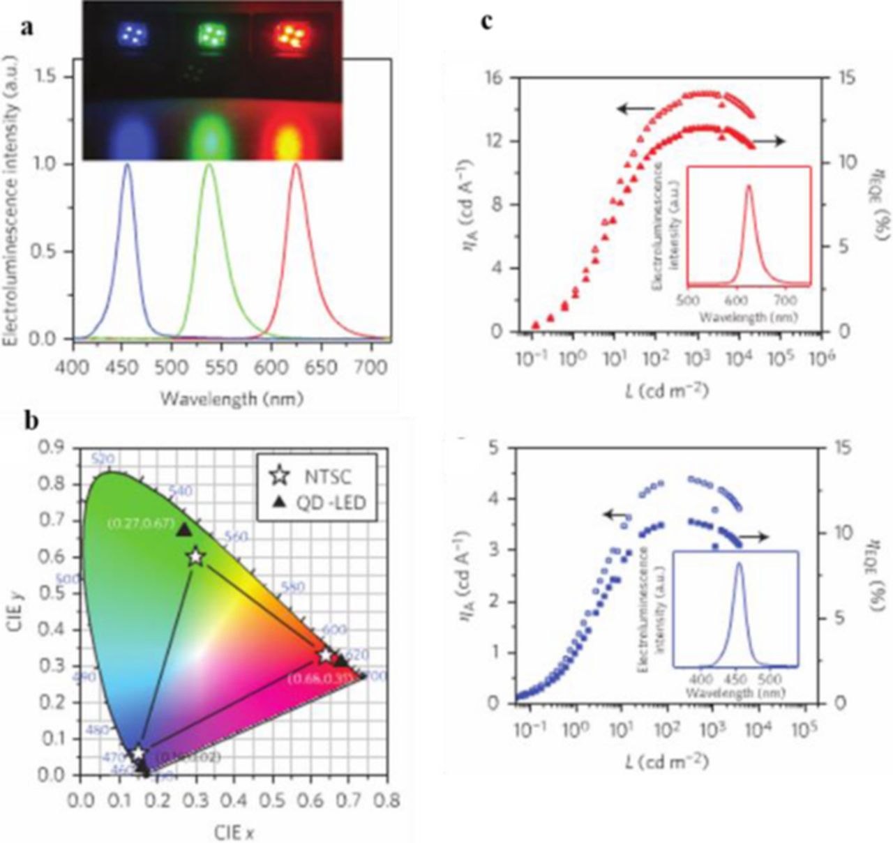
Figure 13. (a) Normalized electroluminescence spectra and images of blue, green and red QD-LEDs. (b) CIE coordinates of the three QD-LEDs (triangles) compared to the NTSC color standards (stars). (c) Current efficiency (ηA) and ηEQE as a function of luminance of the best performing red and blue QD-LED based on quantum dots. Inset: normalized electroluminescence spectrum of the red and blue QD-LEDs. Reprinted by permission from Macmillan Publishers Ltd: Nature Photonics Ref. 28, copyright 2015.
Shen et al. reported blue QD-LEDs with a comparable EQE of 10.3% and a maximum ηA of 1.3 cd A−1.29 This QD-LED is fabricated using ZnCdS/ZnS graded core-shell QDs with 1-octanethiol capping ligands. These capping ligands are shorter than the previously used oleic acid, and allow for an increase in charge mobility. Evidence for this is given by the low turn-on voltage of about 2.6 V and a maximum luminance of 7600 cd m−2 (Figure 14).
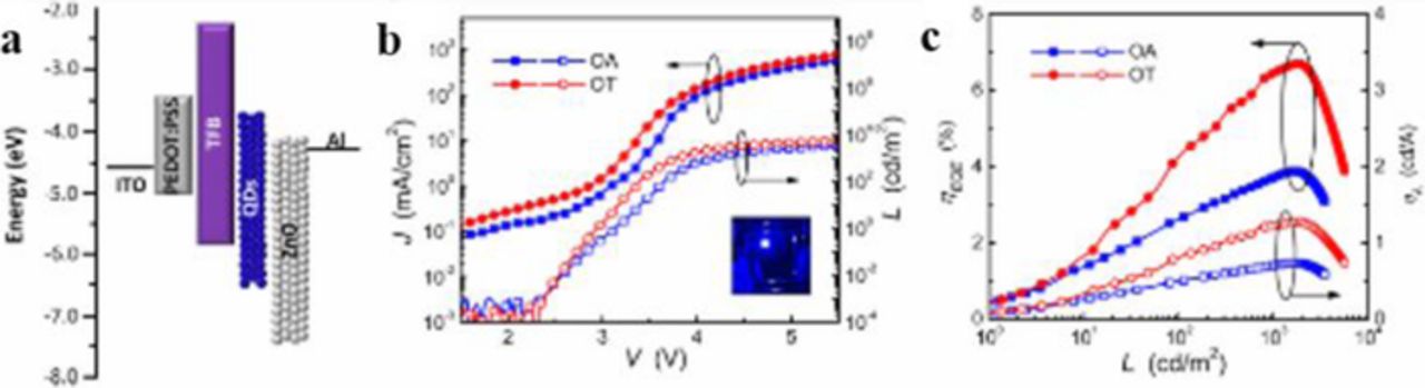
Figure 14. (a) Schematic illustration of energy levels for the multilayer QD-LEDs. (b) Current density (J) and luminance (L) of the devices based on QDs with OA and OT ligands as a function of driving voltage (V). (c) External quantum efficiency (ηEQE) and current efficiency (ηA) of these devices as a function of L. Reprinted with permission from Ref. 29. Copyright 2015 American Chemical Society.
Displays
In 1953, the National Television System Committee (NTSC) developed one of the first color standards that tracked color separately from brightness.30 This standard was based on the best cathode-ray-tube materials available at the time, although it was not until the 2010s that this standard was able to be fully met. In many smaller devices, OLED displays can now exceed this color standard, although this technology has been slow to move toward larger systems. This is due to the lower cost of production of LCDs. Although LCD displays dominate in the display market, they can only reach about 70% of the color performance of OLEDs. LCDs can reach the sRGB color gamut at best because of the white LEDs that are used as the backlight to illuminate the liquid crystal module (LCM). There are millions of pixels that are divided into three subpixels (red, green, and blue) in the LCM. The color of the subpixel is controlled by the efficiency of the filter and of the spectral energy of the white light from the backlight. To make a high quality color, the filter either needs to be very narrow, which will let less light through, or the specific color component from the white light must be narrow and tuned to the desired wavelength. The LED light source does not meet the requirement for narrow color peaks. Quantum dots can solve this problem owing to their narrow emission and high quantum yield. QD Vision and Nanosys are currently developing products that can easily be placed in existing LCD manufacturing. The quantum dots are packaged into either a tube (QD Vision) which is placed adjacent to edge-lit LEDs, or in a film (Nanosys) on top of the LED backlight. Recently, quantum dot LEDs are being researched as the backlight in displays. Kim et al. fabricated a full color QD display using a solvent-free transfer printing method to pattern the individual red, green, and blue emitting QDs onto the pixelated display panel.31 Previous methods of patterning QDs onto the pixels, such as spin-coating, cause a cross-contamination between the three sizes. Other methods lead to non-uniform films with a rough surface. This results in a decrease in the charge transfer and a decline of quantum efficiency. In the transfer printing method, QDs are spin-coated onto a surface modified donor substrate, followed by the application of a polydimethylsiloxane (PDMS) stamp to the QD film. Due to the surface energy of the stamp being less than that of the donor substrate, with sufficient pressure, the QDs are picked up. The QDs are then transferred to a device stack into an array of narrow stripes. Compared to a film that was fabricated using a spin-coated method, the density of the printed film has a 20% greater density of QDs. When integrated into an organic/inorganic hybrid LED structure, the printed red, green, and blue QDs had brightness values of 16,380, 6,425, and 423 cd m−2 and current efficiencies of approximately 3.00, 0.55, and 0.05 cd A−1, respectively (Figure 15). These values are about 25–52% greater than the values collected with the spin-coated device. The method of QD printing was employed to produce a 4-inch full-color active matrix QD display that showed a near perfect image. Due to the elastomeric PDMS stamp, this printing method can transfer QDs onto flexible substrates, which is necessary for scaling up to a roll-to-roll system.
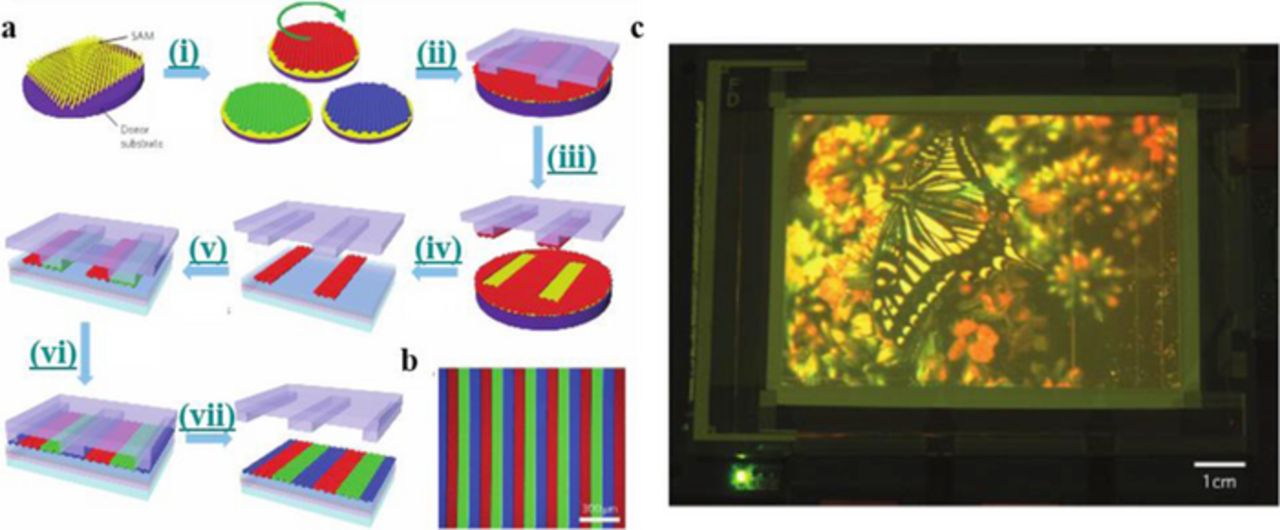
Figure 15. (a) Schematic of transfer printing process for patterning of quantum dots. (b) Fluorescence micrograph of the transfer-printed RGB QD stripes onto the glass substrate, excited by 365 nm UV radiation. (c) Electroluminescence image of a 4-inch full-color QD display using a HIZO TFT backplane with a 320 × 240 pixel array. Reprinted by permission from Macmillan Publishers Ltd: Nature Photonics Ref. 31, copyright 2011.
As previously noted, Yang et al. fabricated red, green, and blue LEDs with EQEs greater than 10%.28 In the report, the red and green QD-LEDs were then fabricated into 4.3 inch monochrome active matrix displays with a resolution of 480 × 800 on low-temperature poly-silicon (LTPS) thin-film transistor backplanes as a preliminary demonstration toward the application of QD-LEDs in displays.
Biological Applications
QDs as biological labels
Quantum dots exhibit several characteristics that make them appropriate for biological applications. As previously stated, they demonstrate broad excitation, narrow size-tunable emission and a strong resistance to photobleaching, making them preferable to conventional organic dyes for long term data collection.32
The synthesis of QDs results in surface-bound organic nonpolar ligands that are not biocompatible. Surface modification is required before the QDs are viable. Initially, surface modification was done through ligand exchange, as seen in Rosenthal et al. 2002.33 TOPO surface ligands of CdSe/ZnS core shell QDs were first exchanged with pyridine in order to allow attachment of serotonin-based linkers for serotonin transporter protein labeling. The QDs were further modified by the addition of mercaptoacetic acid, a short polar ligand. Electrophysiological measurements were taken to show binding of these serotonin-linker arm conjugated nanocrystals (LSNACs). However, the exchange of the surface ligands results in fluorescence quenching; in this example the QDs went from 38% fluorescent quantum yield to 3% after all modifications.
To overcome this fluorescent quenching, an amphiphilic polymer was added instead to both encapsulate the nonpolar ligands without displacement and have polar reactive groups exposed on the outer surface.34 Also of note is the addition of poly-ethylene glycol (PEG) chains to the surface of the QDs. While amphiphilic QDs increase solubility, Bentzen et al. 2005 found that surface addition of PEG chains reduces nonspecific binding during live cell labeling.35
QDs can be functionalized with terminating groups on surface ligands such as carboxylic acid, azide, amine or streptavidin/avidin protein. Carboxyl dots can be conjugated to amine terminated molecules, while amine dots can be conjugated to either amine or thiol-terminated molecules. One of the most prolific applications involves binding streptavidin/avidin conjugated QDs to biotinylated terminated molecules. CdSe/ZnS core shells are available commercially for imaging and can be purchased with surface streptavidin for bioconjugation.36
These well characterized constructs allow for cellular labeling using antibodies,37 peptides/proteins,38–40 sugars41 or small molecules42–44 in fixed and unfixed cell and tissue cultures. Both intracellular and extracellular labelling has been accomplished, with extracellular labeling resulting in more specific binding due to ability to wash away unbound QDs.45 Surface proteins with a revealed extracellular component can be labeled specifically through use of antibodies, through either an exposed amino acid sequence, or, in the case of extracellular termini, through use of encoded fusion tags such as GFP.46 Additionally, small molecule-functionalized QDs can be anchored to an activation site or binding pocket.33,43 The Rosenthal group specializes in such small molecule functionalization in order to visualize and track neurotransmitter transporters (Table I), starting with the synthesized LSNACs33 and then making use of commercially available AMP-QDs for muscimol-QD conjugates,47 and finally taking advantage of streptavidin-coated QDs for easy labeling with biotinylated ligands.48–50
Table I. Small molecules used for neurotransmitter transporter labeling.
| Name | Target | Small molecule structure | QD surface ligand |
|---|---|---|---|
| Serotonin (LSNACs)33 | SERT | 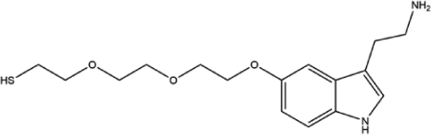 | TOPO |
| IDT31843,48 | SERT |  | Steptavidin |
| Biotin-GBR1290949 | DAT | 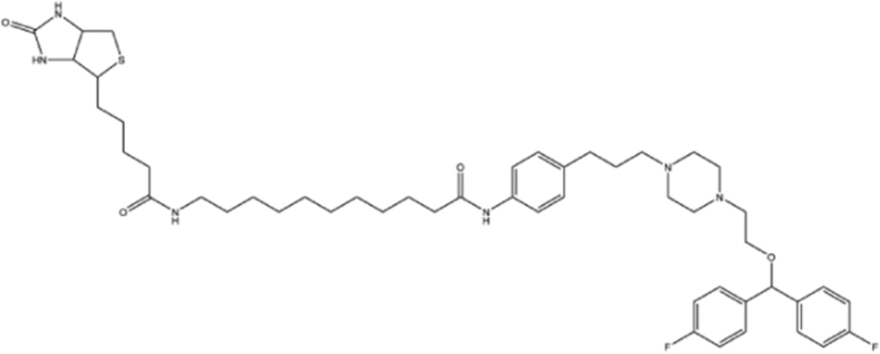 | Steptavidin |
| IDT44450,51 | DAT | 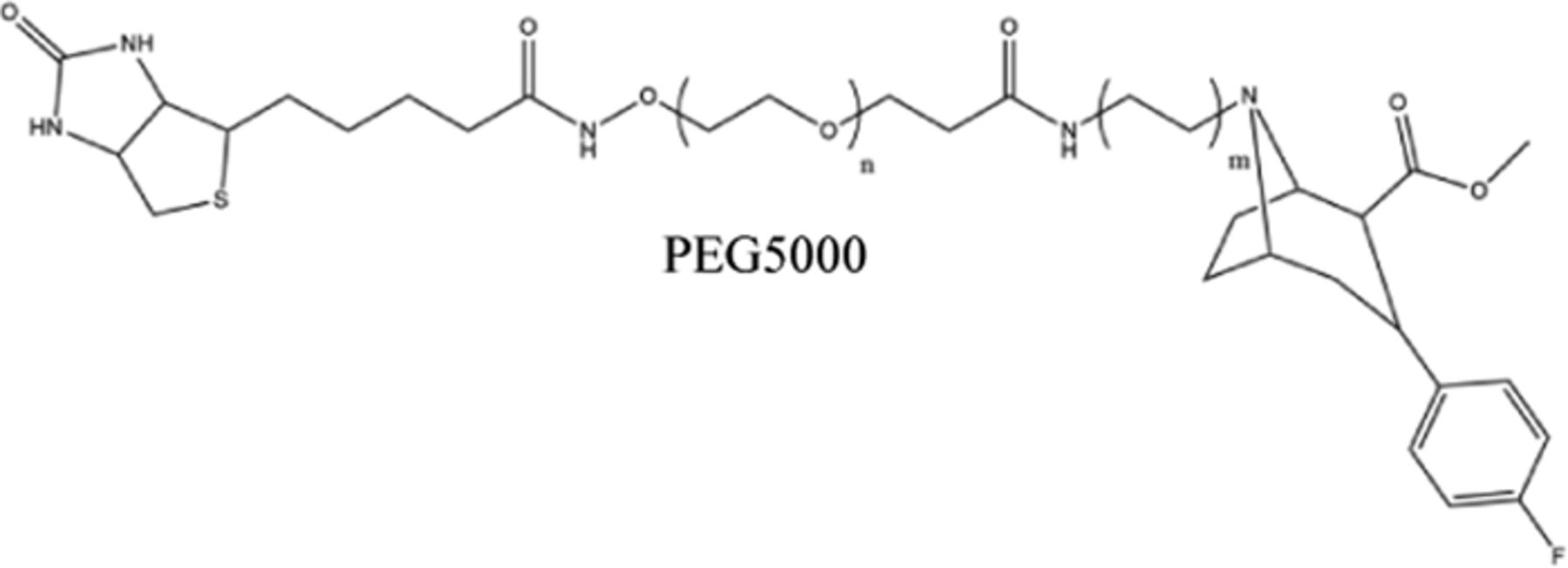 | Steptavidin |
| Muscimol47 | GABA |  | Carboxyl-AMP |
In order to label intracellular structures, the cells need to elicit endocytosis of the QDs. Nonspecific uptake has been studied using transferrin-conjugated QDs in an attempt to study cancer markers,52 while specific labeling of cytoskeletal actin has been done using lipid-associated phalloidin-conjugated QDs to penetrate living cells.53 However, intracellular quantum dots are susceptible to endosomal trapping and aggregation, and difficulty in distinguishing bound and unbound probes.45,53
QDs as dynamic trackers for biological events
In live cells and tissue cultures, QDs can be used to dynamically track different cellular targets and events. The bright emission of QDs allows for estimation of the probe down to a pixel resolution, and easy determination of the position of individual labels which can then be mapped. Unlike organic dyes, the photostability of QDs allows for both longer and more detailed trajectories to be obtained.54 The method of obtaining trajectory data is described in Figure 16.55
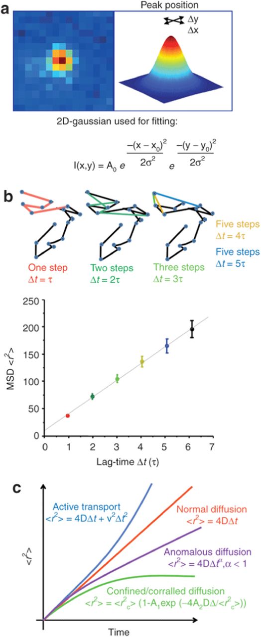
Figure 16. (a) A Gaussian fit of intensity is used to determine location of particles from a timelapse series. (b) the x and y positions derived from the Gaussian fit allows for the construction of a trajectory with positioning related to Δt, allowing for plotting mean square displacement (MSD) as a function of time. (c) The fitted slope of MSD vs time allows for determining the mode of diffusion, where a linear slope denotes a normal or Brownian diffusion. Reprinted by permission from Macmillan Publishers Ltd: Molecular Therapy Ref. 54, copyright 2011.
The construction of trajectories allows for statistical analysis of molecule displacement, velocity, and diffusion coefficient. Mapping mean-square displacement as a function of time, allows for the determination of diffusion mode.56 This allows for quantitative analysis of the cellular targets, and defining the diffusion mode allows for insights into the functionality of the target both natively and in response to stimuli. An example of this is confined mobility seen in membrane compartments or a directed motion seen in motor proteins.42
In 2003, the first single protein tracking using QDs studied the 2D diffusion dynamics of glycine receptors in spinal neuronal cells.57 The Rosenthal group has since used QDs to study the membrane dynamics of the dopamine and serotonin neurotransmitter transporters (DAT, SERT) and their relationship to signaling pathways, such as lipid raft membrane domains and kinase activation pathways.58,48,50 They found that DAT and SERT demonstrate confined diffusion, due to localization with lipid raft membrane domains and as such will exhibit increased mobility when the domains are disrupted.48,50 In addition, variants of the wild-type proteins can be tracked to correlate functionalization and mobility,50
QDs can also be used to study endocytic trafficking, such as Li et al. demonstrating the effect from Paclitaxel exposure on the rate of uptake of epidermal growth factor in cancer cells.44
Biermann et al. has demonstrated short trajectory tracking of glycosylphosphatidylinositol (GPI-anchor)-GFP mobility in organotypic mouse brain slices.37
Drug delivery applications using QD-FRET-based nanosensors
Developing more efficient and precise disease detection and drug delivery systems leads to timely and accurate diagnoses and subsequent treatments. Recently, nanomedicine, and specifically quantum dots, has emerged as an alternative to traditional drug delivery and sensing approaches that exploits QD properties such as brightness and photo-stability, size-tunability, and multi-functionality, incorporating a variety of drugs and ligands on the surface.59 One popular QD-based approach includes using QDs in conjunction with Förster resonance energy transfer (FRET) as a nanosensor system. FRET involves the transfer of electronic energy from a donor chromophore to an acceptor chromophore.60 This transfer occurs through intermolecular dipole-dipole interactions over distances as small as 10 Å to 100 Å, making it an ideal tool for determining distances between biological molecules, for acting as a sensor when two fluorophores are present and interacting, and for confirming that drugs have reached their target locations. QDs are typically used as donors in FRET interactions, as emission intensity changes can easily be quantitated in the presence of acceptor molecules.61 The narrow emission spectra, the diverse surface functionalization capabilities, small size, and brightness of QDs have made them ideal donor molecules for use in FRET-nanomedicine applications.
Zhang et al. used single quantum dots conjugated to DNA probes to detect DNA implicated in genetic diseases.62 They take advantage of a single-strand DNA "capture probe" labeled with biotin that binds to a streptavidin-coated QD, and the target DNA sequence becomes sandwiched between this sequence and another single-strand DNA reporter probe, which also includes a fluorophore (Figure 17). When the DNA target is present, the QD, which acts as a donor, is brought into close proximity with the acceptor, which is the reporter probe. The QD can then non-radiatively transfer energy to the acceptor, and the acceptor emits a photon, allowing for easy confirmation that the DNA target is present. As expected, in the absence of the acceptor, the FRET efficiency is zero, since all of the fluorescence is from the donor. As acceptor/donor ratios increased, so did the FRET efficiency, confirming the presence of the DNA target of interest. In another application, Bagalkot et al. use a QD-aptamer with a fluorescent drug loaded into the aptamer.63 When the drug is loaded onto the QD, both the QD and drug are in the "off" state due to a FRET interaction. The aptamer serves to specifically target the cancer cells, and the particle is then taken up into the cell. Once the drug is released from the QD, both the QD and the drug are fluorescent again, as the FRET interaction can no longer take place. This fluorescence confirms that the drug has reached its target. This design offers the potential to revolutionize the way specific diseases, including cancer, are treated. Prasuhn et al. take advantage of two QD-conjugated dye-labeled peptides to detect caspase 3, a protease of interest in cancer research, and calcium ions, which are critical in many biological pathways.64 When caspase 3 is present, the peptide is cleaved from the QD, disturbing the FRET interaction, resulting in QD emission. Alternatively, when calcium is present, it increases dye emission of the peptide. These applications utilize straightforward chemistries that can be applied to other molecules and ions of interest, making this a diverse and relevant method.
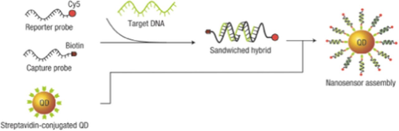
Figure 17. Zhang et al. design a QD nanosensor using a fluorescent reporter probe that has a FRET interaction with the QD when the target DNA is present. Reprinted by permission from Macmillan Publishers Ltd: Nature Materials, copyright 2005.
QDs will continue to be a material of choice for biosensing applications. Their large surface area allows for multivalent functionalization, increasing FRET signal and allowing for widespread applications. Unique QD functionalization and chemistries will continue to evolve, offering widespread applications as nanosensors.
Specific targeting for in vivo imaging
One advantage to having specifically binding QDs includes targeted tumor imaging. In vivo targeting is advantageous to in vitro targeting as it provides more complex information about the natural environment of the protein of interest. Zhang et al. have synthesized specific CdTe: Zn2+ QDs functionalized with a phosphorothioate DNA aptamer with a targeting sequence.65 These QDs target lung cancer tumors in vivo for easy and specific tumor identification. Non-aptamer QDs show no signal, further confirming specificity. These QDs offer exciting possibilities for advancements in disease detection and eventual treatments. Han et al. conjugate tetrazine-modified antibodies to quantum dots passivated with a polyimidazole ligand including norbornene, which maintains an overall neutral charge, decreasing nonspecific binding.66 Using their design, they target a rare cell population in bone marrow at the single cell level in live animals using multiphoton microscopy. The advantages to their QD design include high stability and quantum yield in vivo, low nonspecific binding, compact size, and easily adaptable for a variety of targeting antibodies.
Summary and Future Prospects
With the enhancements in stability, brightness, and water solubility, the commercialization of quantum dots has been on the rise in recent years. QD Vision, founded in 2004, is focused on producing nanomaterials for the use in lighting and display technologies. Most recently, they have released their quantum dot-based Color IQ technology. With a color performance that achieves 100% of the NTSC standard compared to 60–70% from most mainstream LCD designs, quantum dots are ideal for use in TV displays. At the 2015 Consumer Electronics Show, QD Vision along with TCL Multimedia debuted the first quantum dot based TV, TCL 55'' 4K UHD.67 Nanosys, founded in 2001, is producing a Quantum Dot Enhancement Film, QDEF, which is compatible with current LCD displays as a replacement backlight film (Figure 18). At a fraction of the cost, this product exceeds the color output and efficiency of OLEDs.30
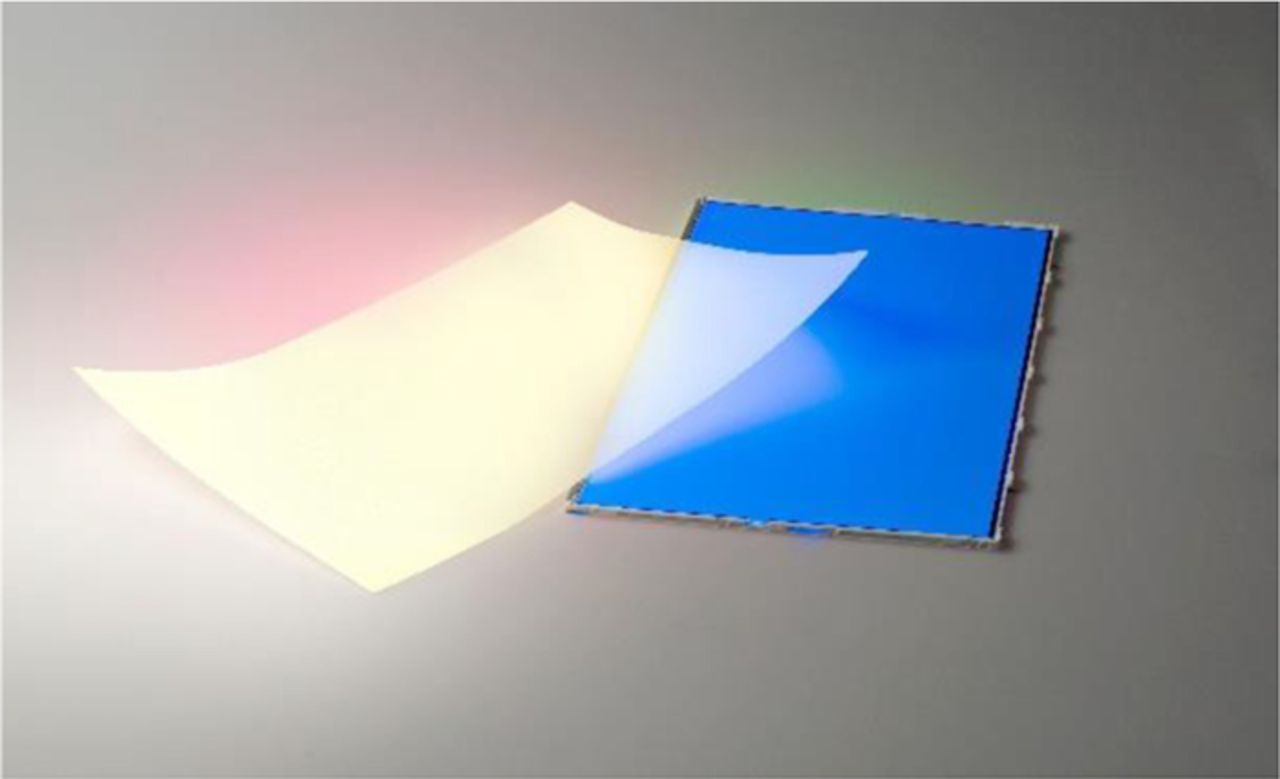
Figure 18. A sheet of QDEF (left) can be seen converting some of the blue light emitted by a BLU (right) into white. Reprinted with permission from Ref. 30.
In addition to being commercially produced for display and lighting technologies, quantum dots are also utilized as fluorescent probes in biological assays. Life Technologies produces standardized aqueous QDs with various functional groups depending on biological labeling need. Standard functionalization includes amino- and carboxyl- terminated ligands, surface streptavidin, surface biotin, or antibodies.36
Precise control of emission
As could be seen by Rosson et al., performing a post-synthesis treatment on the ultrasmall white light-emitting CdSe changed the emission intensity of the energy state correlated to the surface ligand.15 It has been shown that for ultrasmall sizes of CdSe, the emission is no longer controlled by band edge emission, but is pinned at a specific energy.14 In 2009, Schreuder et al. reported a tunability of the wavelength of the pinned emission by varying the electronegativity of the alkyl phosphonic acid surface ligand.68 As the alkyl chain length was increased, the wavelength of the pinned emission blue shifted from 425 to 445 nm, due to the decreasing electron withdrawing nature of the ligands on the adjacent dangling bond of the Cd. Varying the alkyl phosphonic acid chain length also led to a change in the quantum yield of the QDs. As the chain length decreased, the quantum yield also decreased. This may be due to the stronger bond between the Cd and the ligand leading to few ligands being removed during the cleaning process, and preventing trap states from forming. By applying the knowledge of the effect of ligand electronegativity and the increase in quantum yield with a post-synthesis treatment, precisely tuning the emission spectrum of the ultrasmall white-light emitting CdSe QDs is a possibility.
Correlating atomic structure with optical properties
Recently, Orfield et al. have developed a reliable methodology that enables direct correlation of the optical properties of an individual quantum dot with its atomic structure.69 Commercial SiO2 TEM grids with 8 nm thick were used as support film for both single particle fluorescence and high resolution STEM imaging, while polystyrene spheres were used as fiducial markers. As a proof of concept, commercial QD655 quantum dots were imaged under wide field conditions to measure their blinking behavior. Afterwards, the same quantum dots were identified under Z-STEM condition in an electron microscope and their atomic structures were imaged. A total number of 84 particles were correlated, allowing for first time, direct evidence that stacking faults negatively impact the fluorescence of colloidal quantum dots. An example of some of the correlation data is shown in Figure 19.
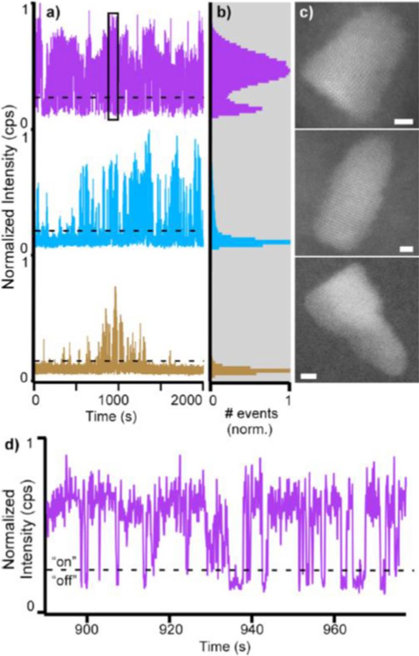
Figure 19. Top: blinking traces and atomic resolution STEM image of the same quantum dots. Bottom: expanded view of the blinking trace in (a) showing the 'on' and 'off' threshold. Reprinted with permission from Ref. 70. Copyright 2015 American Chemical Society.
Additionally, shell coverage was also directly shown to impact a quantum dots 'on time'. Ultimately, this new methodology will accelerate the development of emergent quantum dot systems by allowing for the identification of the best performing structures enabling targeted synthesis strategies. Further, one can specifically design structures with pre-determined blinking rates. Quantum dots with distinguishable on times will open a new modality for single particle tracking experiments.
Summary
As discussed in this review, the stability, brightness, and processability of quantum dots makes them a material of choice for a variety of applications. The quantum dots technologies described above will allow scientists to target problems pertaining to lighting efficiencies and color, display resolutions, and specialized drug delivery and imaging at the molecular level.