
Abstract
The effect of several surface treatments such as chemical-mechanical polishing or plasma activation applied to deposited silicon oxide layer surfaces prior to direct bonding has been investigated. It is shown that these treatments have a direct impact on surface and near subsurface OH bond densities which greatly participate in bonding energy changes. Better understanding of mechanism is proposed even if some conditions still deserve more investigation.
Export citation and abstract BibTeX RIS
Direct bonding is used to join two mirror-polished wafers without any additional material. This technique appears to be more and more used for microelectronics or microtechnologies applications such as 3D and optical integration, MEMS or heterostructure assembly. Silicon oxide (SiOx in which x is lower or equal to 2) deposition is widely used in microelectronics or microtechnologies. Thus it seems very attractive to develop tuned processes of SiOx surface preparation which would allow in many cases using the same layer (e.g. oxide layer) at the bonding interface and avoiding the development of new specific preparation process. One of the main challenges in this study is to obtain efficient bonding of deposited oxide films i.e. high bonding energy values. We will focus hereafter on the study of hydrophilic surface bonding in the low-temperature range (from room temperature to 400°C) of deposited SiOx layers. The nature of the deposited films and the effect of several surface preparations (such as chemical-mechanical polishing or plasma activation) which were applied to deposited films prior to direct bonding were investigated. Main results regarding the bonding strength are reported here.
Experimental
This study was carried out on 200 mm, lightly p-doped Si(100) wafers. Thick silicon oxide films (e.g. 1 μm) were deposited at low temperature (400°C) by Plasma Enhanced Chemical Vapor Deposition (PECVD) with tetraethoxysilane (TEOS) precursor. The two deposited oxides considered hereafter were obtained with different injection systems: liquid direct injection (D.I oxide) and bubbler injection (B.I oxide). In addition, 1 μm thick thermally grown SiO2 oxide layers were used as reference for this study.
After the film deposition or film growth, wafers were submitted to various treatments prior to bonding. For instance Chemical-Mechanical Polishing (CMP) treatments were performed in order to reduce the surface roughness. Also, Reactive Ion Etching (RIE) 13.56 MHz radio-frequency plasma activations under either oxygen or nitrogen atmosphere were also performed in order to clean oxide layer surfaces by a slight etch and activate surface bonds in a dry treatment. After the use of CMP process or RIE plasma activation, wafers were DI water rinsed before bonding. Wafers were bonded at room temperature (RT) in a clean room ambiance with 40% relative humidity (RH). After RT bonding, structures were subsequently annealed at 200°C during 2h in order to strengthen the bonding.
Wafers were characterized before bonding and just after pre-bonding surface treatment by Atomic Force microscopy (AFM) in order to measure the roughness of the deposited film. Fourier Transform Infra Red spectroscopy (FTIR) using the transmission mode was also performed on film right after deposition of after pre-bonding surface treatment. A special focus was made on Si–OH and H2O (bound and free) absorption bands in the [3000–3800] cm−1 range in order to investigate the modification induced on the deposited films by the different pre-bonding treatments. Bonding energy were measured by crack opening method.1 The film bonded structures were also characterized by high energy X-Ray Reflection.2
Results and Discussion
In this paper, evaluation of several surface treatments performed on deposited oxide is reported. In a first part the effects of CMP on deposited and thermal oxide are described, in a second part differences observed for the both deposited oxides and the effect of storage prior to bonding is presented. Then plasma activation is investigated and finally the combination of plasma activation and CMP is exposed.
Impact of CMP on deposited oxide bonding
CMP is routinely used in microelectronic processing to reduce topography of films deposited on patterned surface (e.g. planarization effect). When addressing direct bonding, CMP can be used to smooth surfaces. This enables bonding of wafers with initial high roughness values or with specifically high topology.3 In the case of oxide layers, CMP is very often performed in slurry solution with basic pH. Besides surface smoothing, one of the main effects is to saturate the surface with silanol groups (Si–OH) and induce a "subsurface" hydration. Indeed the pressure applied on the abrasive particle contained in the slurry induces a strain on the oxide subsurface layer enabling water diffusion.4
The root mean square surface micro-roughness was measured by AFM after deposition. For instance in the case of B.I oxide layers, typical as-deposited root mean square (RMS) roughness values of 0.45 nm (1 μm2 scan) were obtained which can be compared to the classic 0.25 nm for thermal oxide layers. This 0.45 nm micro-roughness was shown to be smooth enough to enable direct bonding (referred to "as-deposited" bonding). In this case, wafers were only cleaned with a standard RCA wet process,5 leading to hydrophilic surfaces.
Thermally grown and deposited B.I oxide layer surfaces were also prepared by chemical-mechanical polishing for a subsequent direct bonding (referred to CMP bonding). After CMP process, RMS value of 0.28 nm (1 μm2 scan) was measured by AFM on B.I oxide surface and 0.2 nm for thermal grown oxide.
After post bond annealing at 200°C during 2h, bonding energies were measured for thermally grown and BI oxides considering the two surface preparation conditions: as-deposited surfaces and post-CMP surfaces. The average values of bonding energies shown in Figure 1 are calculated from the measures on several bonded structures. One can observe that bonding energy values are rather low (∼500 mJ/m2) for both the reference and B.I oxide when no CMP process is done prior to bonding. After a 200°C anneal, bonding energy as high as 1.5 J/m2 is reached for the reference and B.I oxide.
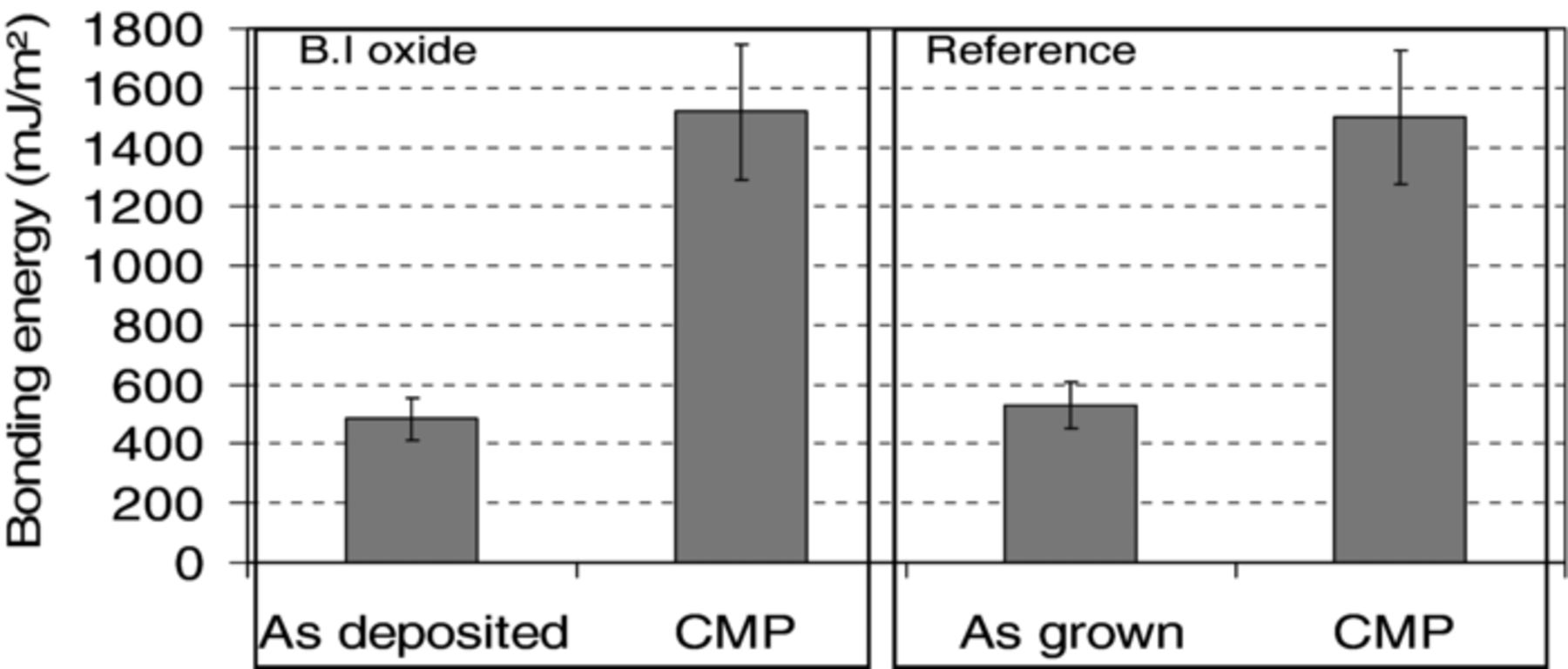
Figure 1. Bonding energy measured after 200°C annealing during 2 hours for thermal grown (reference) and B.I oxides with and without CMP.
The increase of bonding energy whatever the oxide type (deposited or grown) can be attributed to the smoothing effect and the surface activation induced by the CMP process and to the saturation in silanols groups at the oxide surface.
Impact of deposition technique and storage prior to bonding on deposited oxide
Two types of PECVD deposited oxides are compared hereafter to investigate the impact of deposition process on bonding results. These oxides differ by the tetraethoxysilane (TEOS) injection system (bubbler vs. direct injection). Deposition parameters have been tuned in order to obtain SiOx layers (x is lower than 2) with quite similar properties such as dielectric constants (e.g 4.3 +/−0.1), optical indexes... Nevertheless they may differ a little by their in-plane stresses which stay in the slightly compressive [0–100] MPa value range. Prior to bonding, wafers were prepared by CMP just after film deposition or after two months storage in clean room atmosphere.
Measurements of bonding energy value have been done after annealing at 200°C during 2 hours. On the one hand, we notice a difference of 30% in energy values between the two deposition techniques regardless of the surface treatment as shown in the Figure 2. We can thus assume that bonding energy values depend strongly on the oxide deposition technique. On the other hand, we observe that storage time before CMP and bonding led to a more or less pronounced increase of bonding energy values depending on the deposition technique.
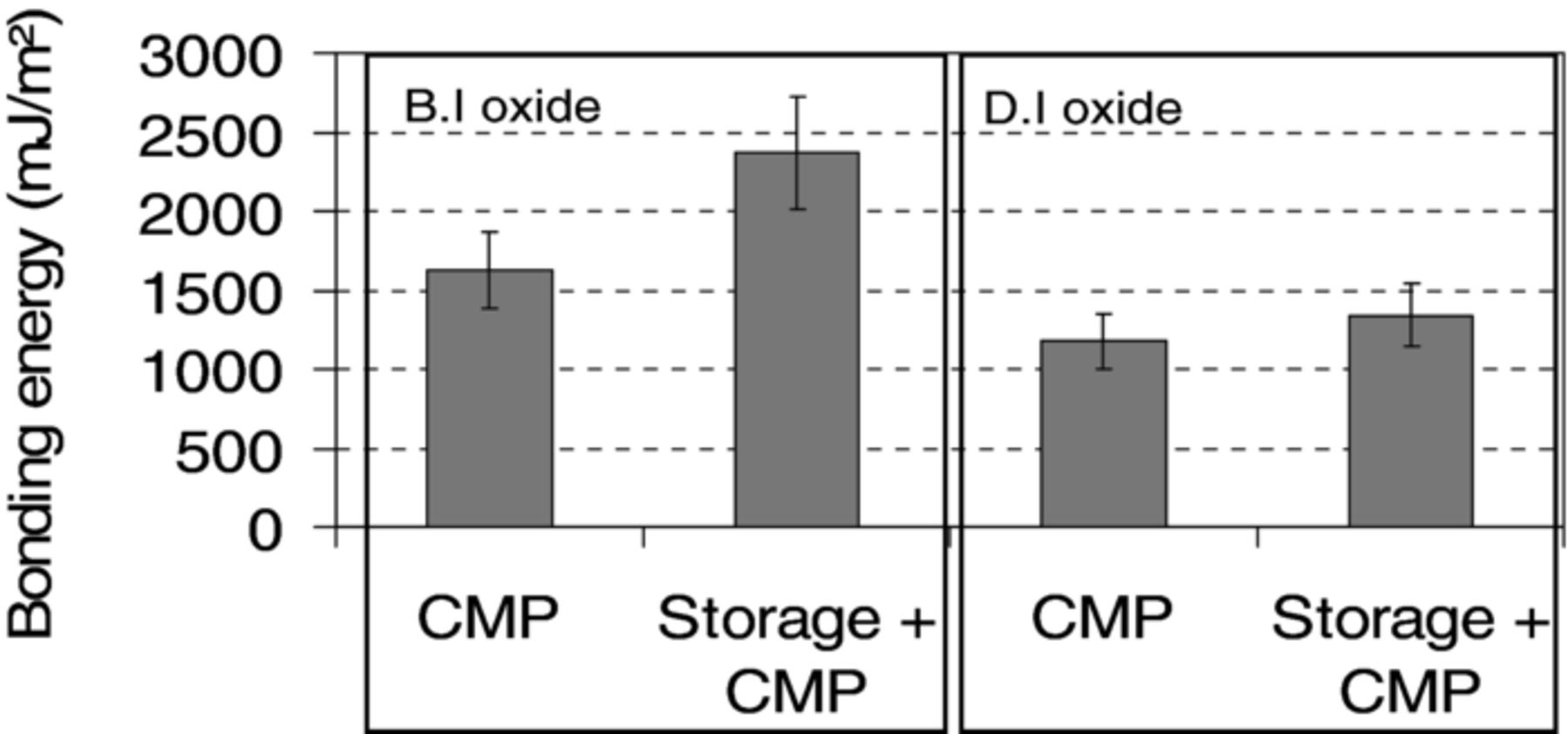
Figure 2. Bonding energy measured (after 200°C annealing during 2h) for B.I and D.I deposited oxide layers. Prior to bonding, wafers were prepared by CMP just after film deposition or after 60 days storage in clean room atmosphere.
Measurements by FTIR spectroscopy in transmission mode were done after film deposition in order to better understand the chemical parameters leading to the difference of bonding energies between the two types of oxide layers. Focus was made on the OH bands which include peaks for silanol Si–OH species (3660 cm−1 for Si–OH groups in the volume, 3540 cm−1 for Si–OH at the surface) and for H2O species (bound water 3400 cm−1 and free water 3225 cm−1). We can assume that peak surface areas are proportional to the quantity of chemical species in the film. As shown in Figure 3, it is worth noting that as deposited DI oxide layers exhibit less water and silanols than BI oxide layers. This could mean the more –OH bonds - either from water or silanol species- the stronger the bonding energies are.6
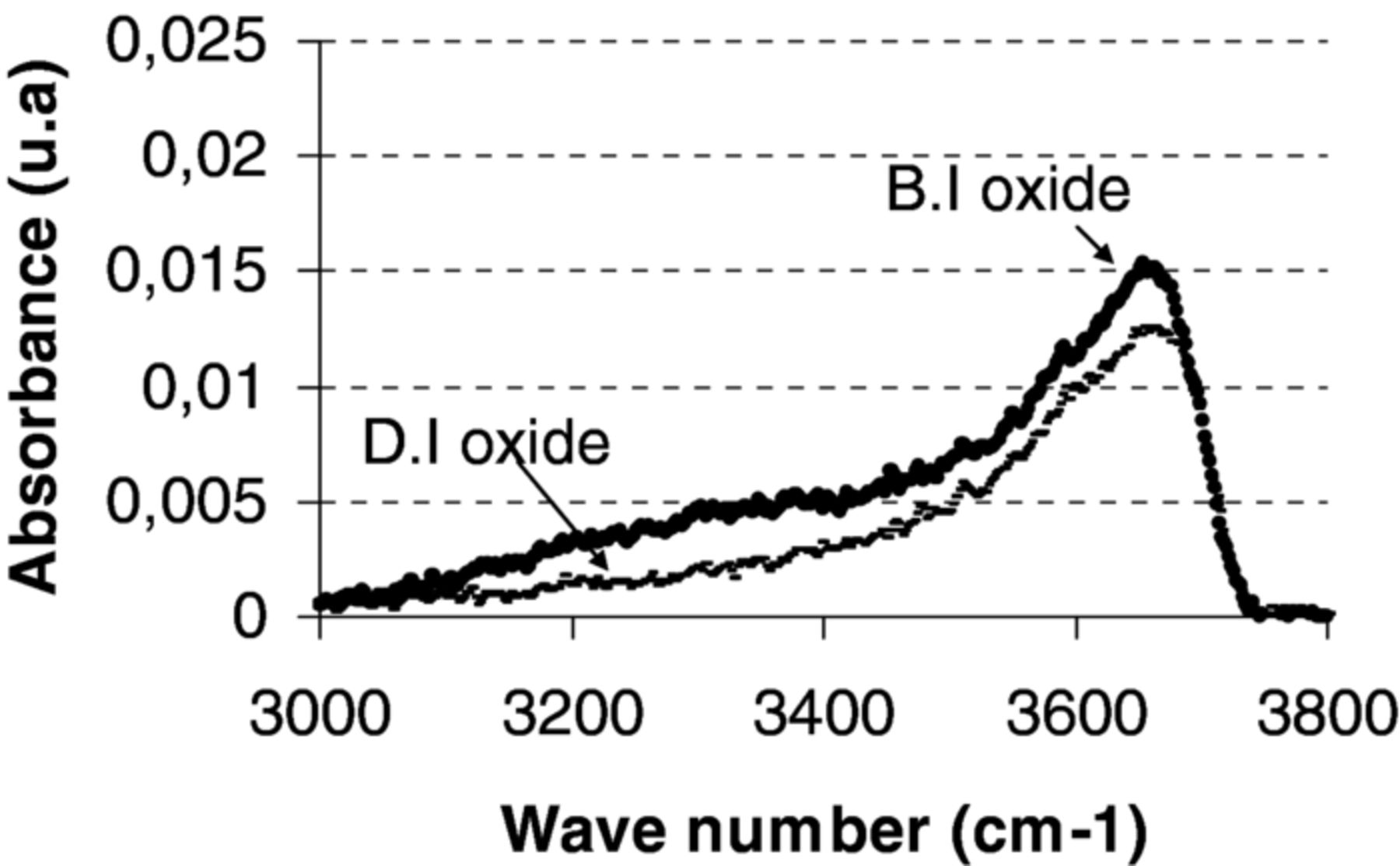
Figure 3. FTIR characterization of Si–OH (in-volume 3660 cm−1, on-surface 3540 cm−1) and H2O (bound 3400 cm−1 and free 3225 cm−1) absorbance band for the two as deposited oxide types.
Furthermore, depending on the aging (storage time and environment) of the film before CMP process, bonding energy values are greatly increased for B.I oxide as shown in Figure 2. The increase in bonding energy is less pronounced for D.I oxide. PECVD oxide layers are known for their ability to absorb moisture when these films are stored in humid environment such as clean room ambiance (RH ∼40%).7
To assess if this absorption of water would have an impact on the bonding strength, FTIR measurements were done several days after deposition (e.g. 40 days) and then compared to results obtained just after film deposition (Figure 4). Again, focus was made on the OH band in order to evaluate the hydration effects of the oxide films as a function of time. The evolution of OH absorption band with storage time of BI oxide layers (Figure 4a) and DI oxide layers (Figure 4b) shows a much stronger increase of the OH absorption band for B.I oxide layers. Therefore, one can conclude that B.I oxide is more sensitive to moisture absorption than D.I oxide. This could be explained for instance by the difference in initial stress between B.I and D.I oxide layers, as-deposited B.I. oxide being less compressive.
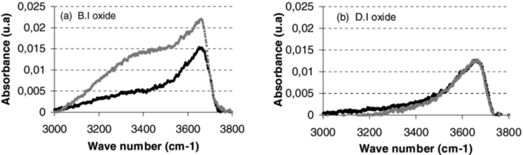
Figure 4. FTIR characterization of Si–OH (in-volume 3660 cm−1, on-surface 3540 cm−1) and H2O (bound 3400 cm−1 and free 3225 cm−1) absorbance band for (a) B.I oxide and (b) D.I oxide two as deposited oxide types as deposited (black line) and after 40 days storage (gray line).
Then, after 60 days storage in clean room environment followed by CMP process, FTIR measurements were performed on the two types of oxide layers. Figure 5 shows FTIR spectra for (a) B.I oxide and (b) D.I oxide after storage, comparing OH band spectra after storage with and without CMP process. Again one can observe that D.I oxide layer exhibits OH band intensity smaller than BI oxide layer which could explain the lower bonding energy measured for bonding made with wafer stored for 2 months (Fig. 2).
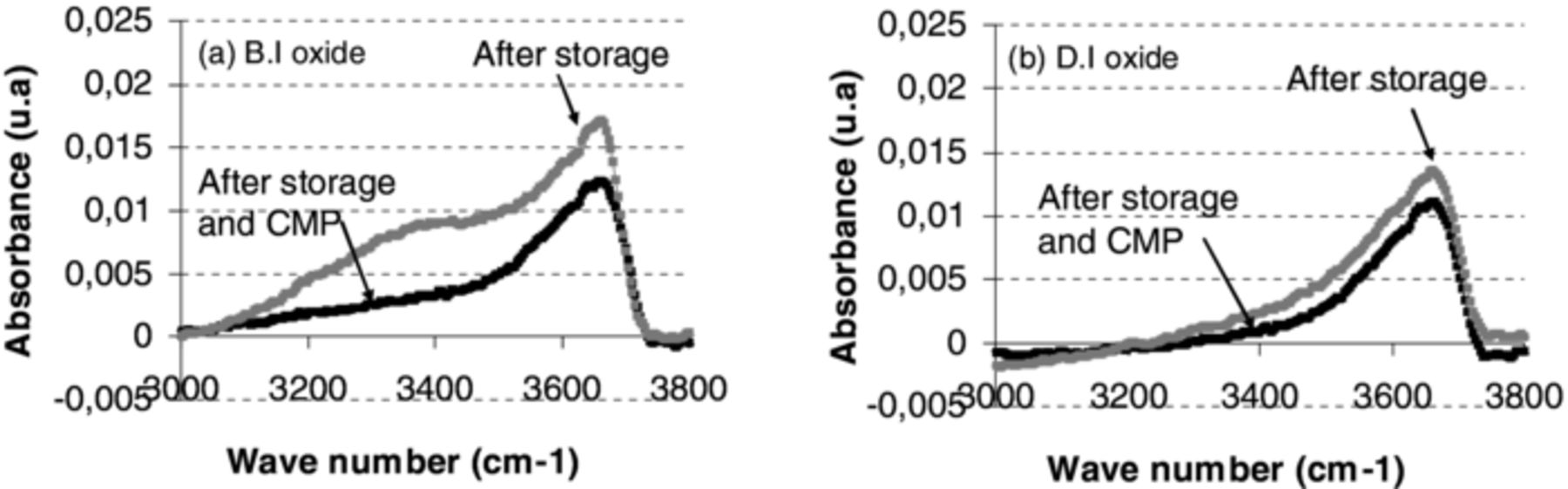
Figure 5. FTIR characterization of O-H absorbance band for (a) B.I oxide and (b) D.I oxide after storage and after storage and CMP, storage time is 2 months.
In the case of B.I oxide film stored for 60 days in clean room environment and followed by CMP process, a decrease of OH band intensity related to water contribution is observed. The add of the CMP process wich induces the removal of a few nanometers thick oxide layer leads to the strong decrease of –OH absorption band, as shown in Figure 5a. It allows understanding that, during the storage time, water had diffused only through the top part of the oxide films, removed by CMP etching.
One can note that focus has been made on the –OH absorption band at room temperature because Si–OH and water (due to surface preparations prior to bonding) are involved in the siloxane bond formation which occurs at the bonding interface during the post bonding annealing (e.g. at 200°C). In the case of bonded structures made of stored and CMP activated surfaces, high bonding energies are obtained after 200°C annealing for 2h (Fig. 2). One can suggest that high densities of silanols combined with small concentrations of water put in evidence at room temperature by FTIR respectively in the [3540 cm−1, 3660 cm−1] and [3225 cm−1, 3400 cm−1] wave number ranges are trapped at or close to the bonding interface and that they may lead to strong bonding energy values after 200°C post bonding annealing.
Impact of plasma activation on PECVD oxide bonding
Previous publications have shown that plasma activations could be used to smooth oxide surfaces, to alter oxide sub-surfaces and to increase silanol densities at the surface.8–10
As shown in Figure 6, activations of thermally grown oxide reference surfaces prior to bonding by O2 or N2 RIE plasma are efficient for increasing bonding strengths after annealing at 200°C for 2h. Thus similar RIE plasma activations under O2 or N2 atmosphere were used on various PECVD oxide layers prior to bonding. Results of bonding energy values are shown in Figure 6 for the B.I oxide type. As observed for reference bonding, RIE plasma under N2 atmosphere is the most efficient to increase bonding energy whereas the use of O2 plasma leads to a slighter increase. Bonding energy values are 4 times higher with N2 plasma, comparing to smaller energy values of "as deposited" B.I oxide bonding.
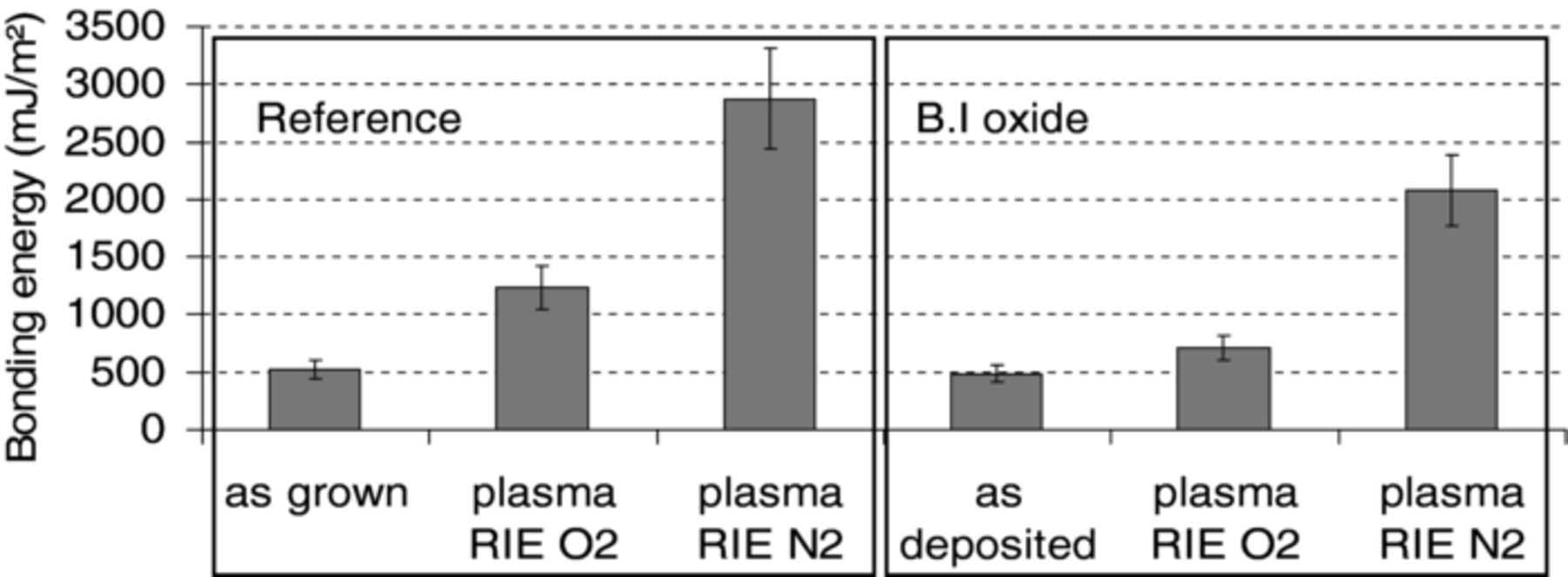
Figure 6. Bonding energy measured after 200°C annealing during 2h for thermally grown (reference) or deposited (B.I) oxide directly bonded or prepared either by RIE O2 or N2 plasma prior to bonding.
In order to understand the parameters leading to such a big difference of bonding energies measured for B.I oxide, FTIR measurement were done just after film deposition and just after RIE plasma activation. Again the focus was made on the evolution of the OH absorption bands.
Figure 7 shows increases of OH absorption bands for activated surface by O2 or N2 RIE plasma. It is worth noting that such increases are observed regardless of the O2 and N2 atmosphere. For the surface activated by plasma, it means that FTIR measurements performed at room temperature are not informative enough to be correlated to bonding energy evolution after annealing at 200°C and that other parameters, such as the physical and chemical parameters of the subsurface layers generated by the plasma treatment, would deserve to be studied into more detail.
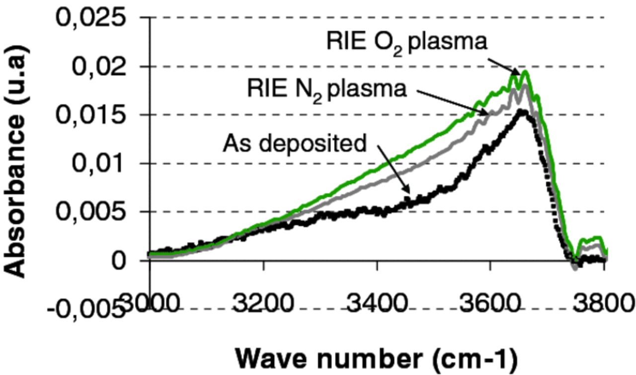
Figure 7. FTIR characterization of O-H absorbance band for B.I oxide types as deposited, after RIE N2 or O2 plasma activations.
Ventosa et al.11,12 investigated the bonding mechanism occurring in the case of thermal oxide bonding. In this study, it was shown that after 200°C annealing, the bonding energy increases while the water trapped at the interface is not evacuated and stays trapped in unbonded zone. The formation of covalent siloxane bonds at the bonding interface leads to an increase of the bonding energy but also to the production of water which is trapped at the bonding interface. When considering the bonding mechanism proposed by Ventosa et al.11 for thermal oxide bonding, the water management at the bonding interface has to be taken into account to understand the mechanism involved in the bonding interface closing.
In the case of deposited oxide surfaces activated by plasma, the management of water should also be taken into account. To explain the increase in the bonding energy, one could assume that the plasma treatment enables the water to diffuse out in the deposited oxide by damaging the subsurface and thus helps for the formation of siloxane bonds at the bonding interface which leads to an increase of the bonding energy.
The RIE N2 plasma seems to be a better candidate to induce physical and chemical modification of the subsurface favoring the water out-diffusion. One could suggest further investigations in order to better understand the bonding closure mechanisms especially comparing the role of divalent oxygen and trivalent nitrogen in bridging chemicals bonds and the damaging effect in the subsurface because of nitrogen or oxygen implantation induced by the RIE plasma.
Use of CMP and plasma as pre-bonding surface preparation
Use of CMP for surface preparation makes sense for applications in which surfaces have been patterned previously to oxide layer depositions. In this case, oxide surfaces need to be CMP-planarized. When planarized surfaces are not immediately bonded, wet surface cleaning or plasma surface activation may be required prior to direct bonding.
Bonding performed using wafers prepared by CMP and subsequent plasma activation was then investigated. As shown in Figure 8, the combination of CMP and N2 RIE plasma activation allows obtaining bonding energy values, after annealing at 200°C during two hours, similar to the ones obtained with surfaces prepared by CMP alone.
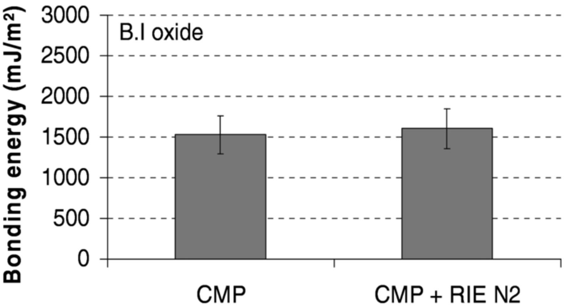
Figure 8. Bonding energy measured after post bond 200°C annealing for B.I oxide bonding prepared by CMP and combination of CMP and N2 RIE plasma activation.
Moreover, effect of long time storage was also investigated. Again increases of bonding energies are observed in the case of 60 day storage followed by CMP surface preparation (Fig. 9 left).
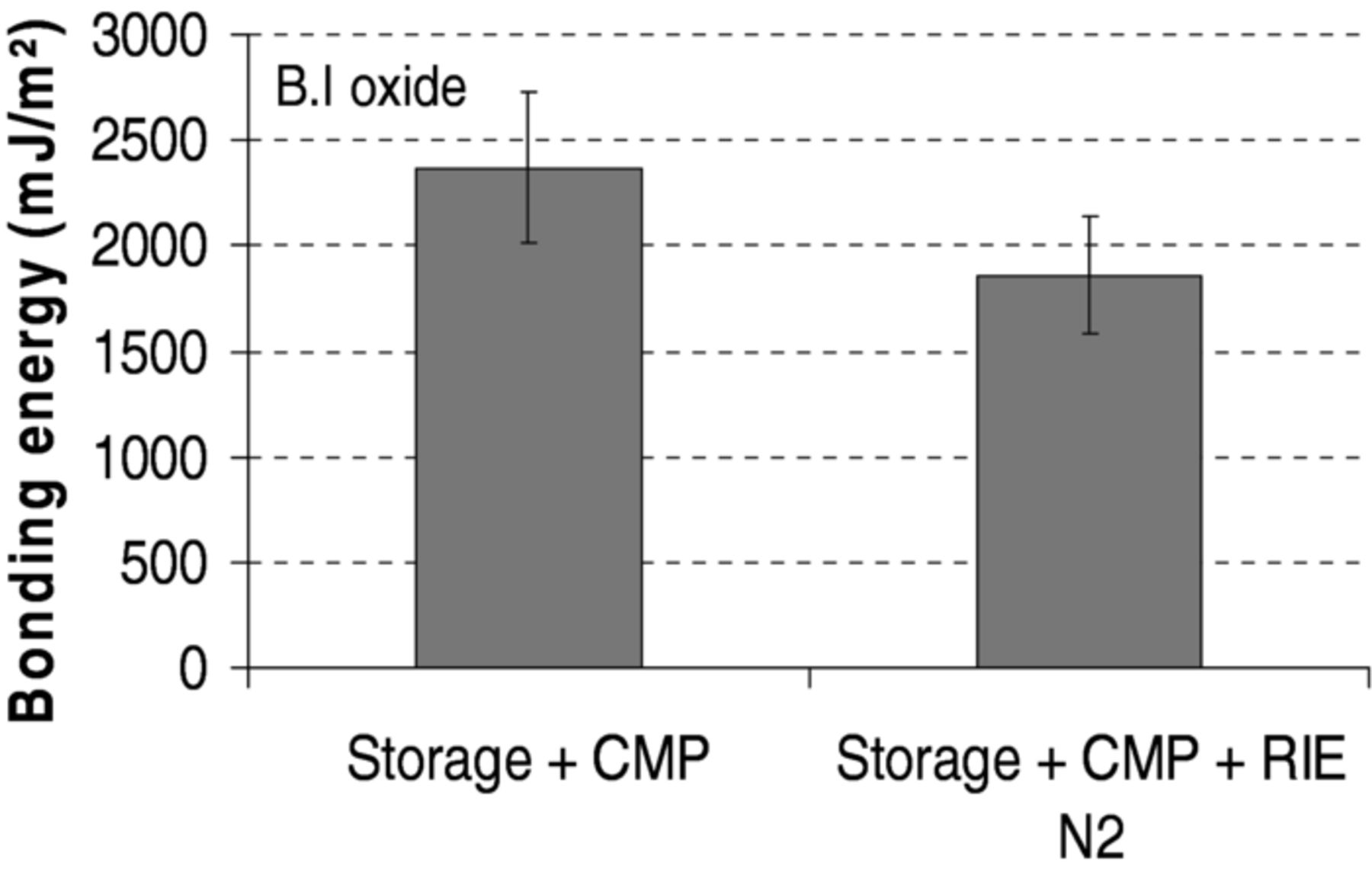
Figure 9. Bonding energy measured after 200°C annealing for B.I oxide bonding prepared by CMP and combination of CMP and N2 plasma after 60 day storage.
At the contrary, one can note that the addition of a long storage period (e.g. 60 days) prior to surface preparation, by the combination of CMP and N2-RIE plasma activation, lead to lower bonding energies (Fig. 9 right).
In order to compare the effect of storage on surfaces prepared by either CMP alone or CMP and N2-RIE plasma, FTIR measurements were performed at room temperature on correspondent bonded structures. Figure 10 shows an increase of OH absorption band mainly in the [3225 cm−1, 3400 cm−1] wave number ranges in the case of surface preparation by CMP and N2 plasma activation after a 60 day storage. This can be linked to a higher concentration of water at or around the bonding interface. In that case, one could suggest that excess of water had been retained at the surface and in the subsurface. As a consequence more water has to be removed from the interface and the subsurface during the post bonding annealing. It may induce less bonded areas and as a consequence a lower bonding strength. Further investigations would be needed to characterize OH band evolution versus post bonding annealing temperatures in order to better understand the impact of N2 plasma activation especially regarding the initial surface and subsurface chemical species.
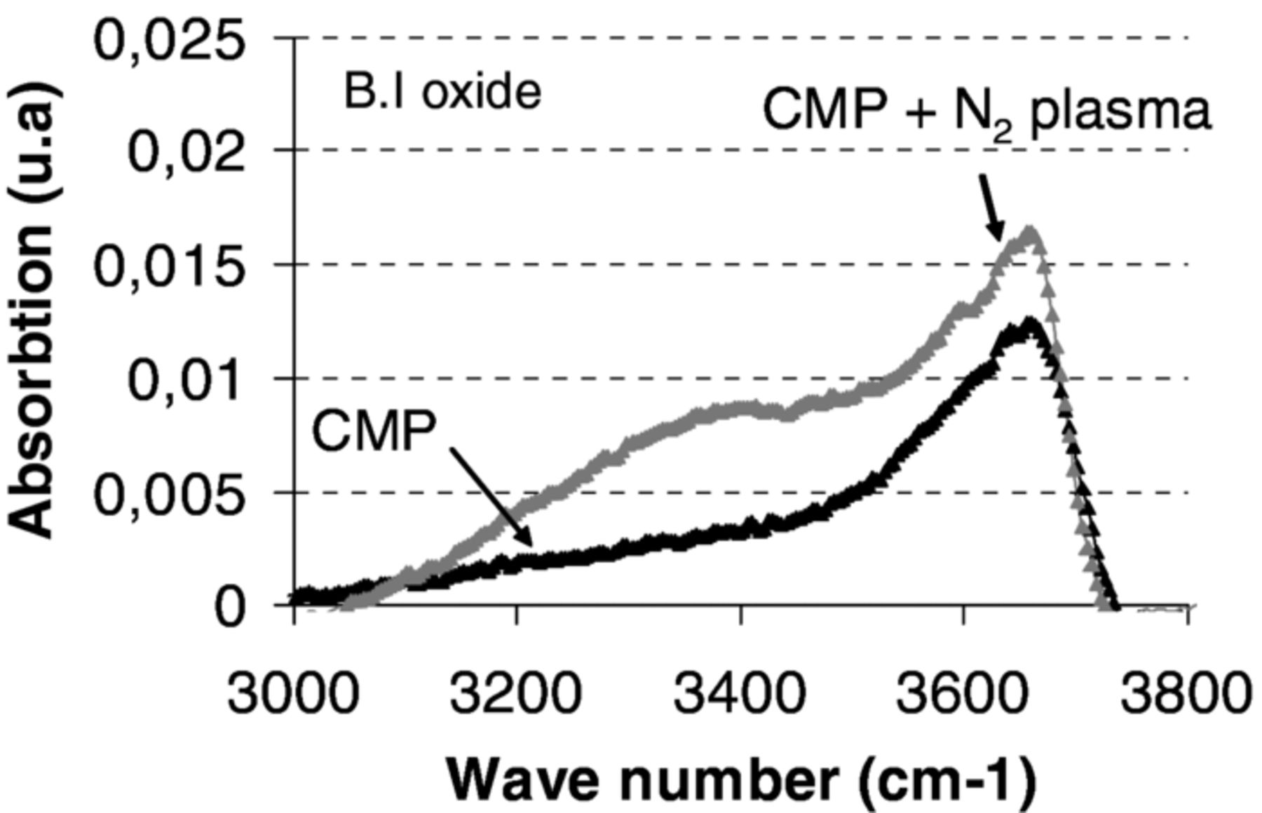
Figure 10. FTIR characterization of O-H absorbance band for B.I oxide measured after CMP (black line) and after CMP and N2-RIE plasma (gray line), after two months storage.
Conclusions
In this article, focus has been made on surface behavior and surface preparation of PECVD oxide layers. Various ways were investigated. Film aging has shown that it could induce –OH bonds increase (either water or silanol) in the deposited oxide film and that, in some cases such, an increase in–OH bonds may lead to increase bonding energies. The second one relies on CMP surface preparations. They allow reducing roughnesses of as-deposited oxide layers, providing activated surface bonds and obtaining highly hydrophilic surfaces. These parameters strongly contribute to bonding energy improvements. Increases by a factor of 3 have been reported. The third surface preparation consists in using N2 plasma activation and can be applied to deposited oxide layers even without the use of CMP. It was shown that it leads to strong increases of bonding energies. Values over 2J/m2 after 200°C annealing are obtainable which is more than 4 times the as-deposited bonding energy. In addition to the use of storage time, CMP or plasma activation have allowed improvements of bonding energies when performed alone. The time storage, CMP processes, and plasma activations have shown their efficiency to enable water absorption and in many cases to allow high bonding energies despite the low temperature used for bonding strengthening. However the combination of storage, CMP and plasma did not lead to any additional improvement yet. Such a behavior deserves to be more investigated. A key parameter to understand bonding mechanisms appears to be the ability to water absorption and the absorbed water concentration. Further analyzes are still required to fully understand the bonding interface closure mechanisms.
Acknowledgments
The authors thank SOITEC S. A. for financial support.