
Abstract
In this work, thin films of phase-pure Cu2ZnSnS4 (CZTS) were developed from a stack of binary metal sulfides by post-deposition thermal processing. The precursor stack SnS/Cu/ZnS was grown by sequential electrodeposition of SnS and Cu layers followed by thermal evaporation of ZnS layer. The transformation from binary/ternary composition to phase-pure CZTS was studied using different experimental tools such as X-ray diffraction (XRD), Raman spectroscopy, scanning electron microscopy (SEM), transmission electron microscopy (TEM), and X-ray photoelectron spectroscopy (XPS). The TEM images revealed the formation of tetragonal crystals with interplanar spacing 0.312 nm. Raman spectra of the films confirmed that annealing at 550°C for 30 min under N2/S ambient resulted in the formation of phase-pure CZTS film. The bandgap estimated from the optical transmittance and reflectance spectra showed a direct transition at 1.59 eV. The films are photosensitive and the photo electrochemical measurements showed the p-type conductivity of the films.
Export citation and abstract BibTeX RIS

This is an open access article distributed under the terms of the Creative Commons Attribution 4.0 License (CC BY, http://creativecommons.org/licenses/by/4.0/), which permits unrestricted reuse of the work in any medium, provided the original work is properly cited.
Kesterite Cu2ZnSnS4 (CZTS) has gained attention as a suitable material for next generation thin film solar cells, competing with Cu(In,Ga)Se2 (CIGS) and CdTe. There are several factors which make this material attractive; abundance of the constituent elements in earth crust, Cu: 25 ppm, Zn: 71 ppm, Sn: 5.5 ppm,1 appropriate direct bandgap of 1.4–1.5 eV, high optical absorption coefficient of 104 cm−1 and a theoretical power conversion efficiency of 32.2%.2–5 Moreover, the absence of toxic and expensive elements highlights CZTS as an alternative to CdTe and CIGS, which is important in high volume manufacturing of photovoltaic panels and its deployment.
CZTS thin films have been deposited by several methods such as thermal evaporation,6 sputtering,7 RF magnetron sputtering,8 electrodeposition,9–12 sulfurization of the metals, binary sulfide or CZTS layers deposited by different methods1,13–16 etc. In majority of the cases, the films were subjected to post deposition thermal treatment to attain stoichiometry and improve the structural and optical properties.
Devices with CZTS and CZTS/Se absorber layers developed by both chemical and physical methods have been reported earlier.17–22 Among the vaccum based techniques, co-evaporated Cu2ZnSnSe4 (CZTSe) and sputter deposited CZTS have attained device efficiencies of 9.15% and 9.3% respectively.18,19 The films developed with chemical methods such as electrodeposition and nanoparticle based suspension are equally competent and economically attractive. Solar cells with 5.5% and 7% efficiencies were reported with CZTS and CZTS/Se absorber layers developed by electrodeposition technique.21,22 All these aforementioned results suggest a potential commercial interest behind sulfide/selenide based kesterite solar cells which need further optimization in the film synthesis and device fabrication steps to compete with established CdTe and CIGS technologies.
In the present work we developed the CZTS films on SnO2:F substrates by the sulfurization of a stack of SnS/Cu/ZnS films under N2/S atmosphere. The SnS and Cu films were developed by electrodeposition whereas ZnS film was deposited by evaporation in the order shown for the stack. The films were annealed at different temperatures in presence of S to identify the optimum annealing temperature for the formation of phase pure CZTS. The crystal structure, composition, morphology, and electrical properties of the CZTS films were examined using different techniques such as X-ray diffraction (XRD), scanning electron microscopy (SEM), transmission electron microscopy (TEM), UV–Vis spectroscopy, X-ray photoelectron spectroscopy (XPS), Raman spectroscopy, photoelectrochemical (PEC), and photoconductivity measurements. We consider the results presented in this paper will update the knowledge on this promising photovoltaic material.
Experimental
Preparation of SnS/Cu/ZnS stack
The first layer of 200 nm thick SnS thin film was electrodeposited on SnO2:F coated glass substrates by pulse electrodeposition (PED) method. The electrodeposition bath contained 2 × 10⁻³ M of SnCl2 and 8 × 10⁻³ M Na2S2O3. The applied potentials were Von = −0.9 V (deposition potential) and Voff = 0.1 V (dissolution potential) vs. saturated calomel electrode (SCE). The details of the electrodeposition of SnS films have been reported in our earlier work.23 The second layer was a 200 nm thick Cu thin film, deposited on SnS film, by applying a constant potential of −0.7 V vs SCE. The deposition was carried out at room temperature from an electrolyte bath containing 100 mM of CuCl2 at pH 2.5. The third layer was 140 nm ZnS deposited by thermal evaporation of ZnS powder (99.9%) in a vacuum system. The film was deposited at the rate of 1 Å/s and the vacuum was maintained at 1 × 10⁻⁵ Torr. The thickness of each layer was optimized to obtain stoichiometric composition for the films.
Thermal treatment of SnS/Cu/ZnS stack
The precursor stack SnS/Cu/ZnS was subjected to heat-treatment ranging from 300 to 550°C in a vacuum oven under nitrogen/sulfur atmosphere (1 Torr) for 30 min. The samples were heated initially at 100°C under vacuum for 5 minutes, and then the temperature was raised to the required point at the rate of 30°/min. Characterization of the films using different techniques showed that the SnS/Cu/ZnS stack annealed at 550°C for 30 min in N2/S atmosphere resulted in kesterite Cu2ZnSnS4 phase. Polycrystalline CZTS thin films with spatial uniformity and good adherence were obtained.
Characterization techniques
The structure of the films was studied from XRD patterns recorded using a Rigaku D/MAX-2000 X-ray diffractometer with monochromatized Cu-Kα radiation (kα = 1.54056 Å). The formation of pure kesterite phase was confirmed from Raman spectra of the films which were recorded using a micro Raman spectrometer (Horiba Jobin Yvon HR800) equipped with an Olympus BX41 microscope and a thermoelectrically cooled charge-coupled detector (Synapse 1024 × 256, pixel size 26 μm × 26 μm). The sample was excited with 632.8 nm line of a He-Ne laser. The laser power on the sample was about 5 mW with spot size of about 3 μm in diameter. The beam was focused on the sample using an objective lens with 50× magnification (numeric aperture: 1). Morphological studies were done using field emission scanning electron microscope (FESEM HITACHI S-5500) and elemental analysis was carried out using an energy dispersive X-ray detector attached with the FESEM. The Scanning transmission electron micrographs (STEM) were acquired by a probe spherical aberration corrected JEOL JEM 2200FS electron microscope operating at 200 kV. All images were acquired in the STEM mode using bright and high angle annular dark field (HAADF) detectors. XPS-data was obtained using a Thermo Scientific K-Alpha XPS instrument with monochromatized Al Kα radiation (hν = 1486.68 eV). The optical transmittance and reflectance spectra of the films were recorded using JascoV-670 spectrophotometer.
Electrical conductivity under dark and illumination conditions was measured using Keithley 230 programmable voltage source and a Keithley 619 electrometer. The electrical contacts were taken from carbon electrode painted on top of the film and from the conducting glass substrate (carbon electrode/CZTS/conducting glass); the area of carbon electrode was 0.20 cm2 (4 mm × 5 mm). The film was illuminated through the glass side using a tungsten halogen lamp at 100 mW/cm2 power. Activation energy was calculated from the I-T data collected under dark in the temperature range 12–296 K at an interval of 0.5 K using a computer controlled Keithley 236 source measure unit. The sample was mounted on the cold finger of a cryostat (Cryogenic Advanced Research systems DE202AE). The PEC measurements were carried out with the same system utilized for electrodeposition of the films except that the electrolyte used was 0.01 M HCl solution. The light source was a tungsten lamp, the sample was illuminated through the glass substrate with an incident power of about 100 mW/cm2.
Results and Discussion
Structure and morphology
The XRD patterns of the CZTS films obtained by annealing the SnS/Cu/ZnS stack at different temperatures are shown in Fig 1a) 350°C, 1b) 450°C, and 1c) 550°C. The X-ray spectra of the films annealed at 350°C and 450°C show the presence of binary phases such as ZnS, SnS, and CuS. However the X ray pattern from the film annealed at 550°C shows the formation of CZTS without any impurity phases (Fig. 1c). The major diffraction peaks at 28.48, 47.3, and 56.18°, corresponding to (112), (220) and (321) planes along with other peaks of relatively low intensity, positioned at 2θ = 18.20, 32.98, 69.22 and 76.44° of (101), (200), (008) and (332) planes of the tetragonal kesterite structure can be observed (JCPDS No. 26–0575). No diffraction lines corresponding to binary compounds such as SnS (PDF 39–0354), SnS2 (PDF 23–0677), Sn2S3 (PDF 30–1379), CuS (PDF 06–0464), CuS2 (PDF 01-072-2276) were observed in the X ray diffractogram. However, in the case of a quaternary compound such as CZTS, a conclusive analysis of phase purity cannot be performed only with XRD, since the diffraction peaks of ZnS and Cu2SnS3 are reported at 2 theta values very close to that of CZTS. Hence we discuss this issue further in the section of Raman spectroscopic studies.
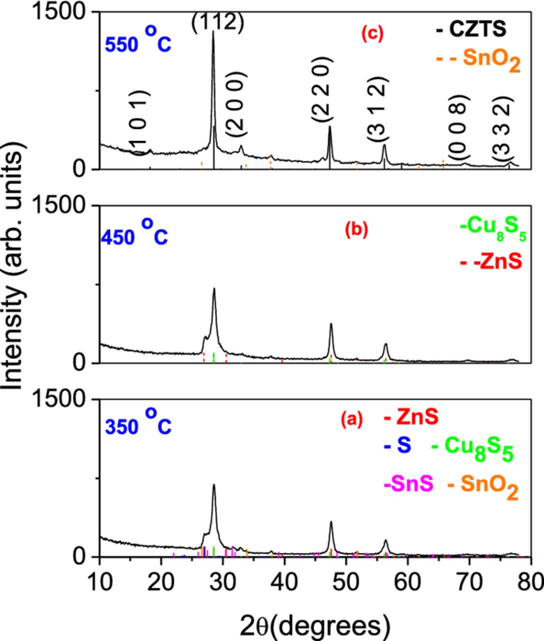
Figure 1. XRD patterns of CZTS films obtained by annealing the SnS/Cu/ZnS stack at (a) 350°C (b) 450°C (c) 550°C for 30 min. For (a) and (b) reference patterns of binary phases such as SnS (PDF 39–0354), ZnS (PDF 36–1450), and CuS PDF 33–0491 are included, and for (c) the standard reference patterns of Kesterite (PDF 26–0575) and the cassiterite SnO2 substrate (PDF 46–0188) are presented.
The average crystalline size was calculated by using the full width at half maximum (FWHM) of the strongest (112) peak in the Scherrer equation  , where D is the crystalline diameter, λ is the wavelength of the incident radiation, k = 0.90 is the shape factor, θ is the Bragg angle, and β is the corrected FWHM in radians, β2 = (FWHM)2 − b2 where b is the line broadening due to instrument, which has been estimated using a powder sample of lanthanum hexaboride. The estimated crystalline size was in the range of 18 nm. The lattice parameters calculated from the XRD pattern of the film were: a = b = 5.426 Å, and c = 10.856 Å which are similar to that described in the literature (a = b = 5.427 Å, and c = 10.848 Å; JCPDS No. 26–0575) for tetragonal kesterite structure.
Raman spectroscopy is a useful tool to confirm the formation of kesterite CZTS material. The Raman spectra obtained for SnS/Cu/ZnS stacks before and after annealing are shown in Fig. 2. Fig. 2a represents the as-deposited stack, while (2b) to (2e) correspond to samples annealed at 350°C, 450°C, 500°C and 550°C respectively for 30 min. The transformation of the binary-metal stack to phase-pure CZTS film is evident from Fig. 2. The resolved bands in the region 200–400 cm−1 for the film annealed at 550°C is shown in the inset of Fig. 2e. As expected, the Raman spectrum of the as deposited stack shows the characteristic Raman bands of binary phases only. On the other hand, the Raman spectra of the films annealed at 350°C and 450°C show the formation of CZTS with main peaks at 337 and 370 cm−1; however, the presence of other binary and ternary phases like Cu2SnS3, Cu2-xS, Cu2O, SnS, SnS2 can also be seen in the spectra. As the annealing temperature was increased to 500°C, we observe the coexistence of ternary (Cu2SnS3: Raman peaks at 280, 306 cm−1) and quaternary (Cu2ZnSnS4: 337, and 372 cm−1) phases in the films (see Fig. 2d). The Raman spectrum of the film annealed at 550°C shows only the bands corresponding to CZTS (Fig. 2e). The strongest peak at 337 cm−1 is identified as the vibrational A symmetry mode of kesterite. The other weaker bands observed in the spectrum at 138, 251, 287, and 368 cm−1 are in good agreement with the reported Raman bands of kesterite.3,24–28 The Raman band positions for different Cu–Sn–S ternary phases and ZnS binary phase are as follows: Cu2SnS3 (CTS) tetragonal phase has characteristic bands at 297, 337 and 352 cm−1; bands at 267, 303 and 356 cm−1 are of cubic CTS; monoclinic CTS phase has characteristic bands at 290 and 352 cm−1; and band at 318 cm−1 indicates the presence of Cu3SnS4 (orthorhombic), while for ZnS the band corresponding to the cubic phase is at 348 cm −1 and for hexagonal phase at 356 cm−1. Absence of all the above mentioned bands in the Raman spectrum of the film annealed at 550°C confirms the phase purity of the material. The Raman peaks of possible binary, ternary, and quaternary phases of Cu-Sn-Zn-S system with its references are given in Table I. As we have seen that the kesterite CZTS layer has been formed by thermal treatment of SnS/Cu/ZnS stacks at 550°C for 30 min in N2/S atmosphere, further structural, optical and electrical characterizations were performed only with that film.
Table I. Raman peak positions of CZTS, ternary and binary phases.
| Phase | Raman scattering bands (cm−1) | Reference |
|---|---|---|
| CZTS | 289, 338, 351, 370 | 24–28 |
| Cubic ZnS | 348 | 27 |
| Hexa-ZnS | 355 | 29 |
| SnS | 96, 163, 189, 220, 288 | 30 |
| SnS2 | 315 | 30 |
| Sn2S3 | 32,60,307 | 30,31 |
| Cu2-x S | 475 | 32,33 |
| Cubic Cu2SnS3 | 267, 303, 356 | 27,34 |
| Tetrg.Cu2SnS3 | 297, 337, 352 | 27,34 |
| Monoclinic Cu2SnS3 | 290, 352 | 34 |
| Ort.Cu3SnS4 | 318 | 27 |
| Cu2Sn3S7 | 268,318, 375 | 35 |
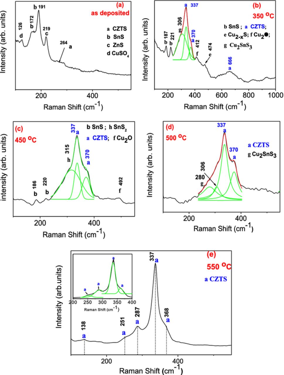
Figure 2. Raman spectra of SnS/Cu/ZnS stack: (a) as deposited, and annealed for 30 min at (b) 350°C, (c) 450°C, (d) 500°C, and (e) 550°C.
The SEM image of the phase-pure CZTS film is shown in Fig. 3. As can be seen the film is formed by closely packed agglomerations of crystallites, spatially uniform and granular with exception of few defects. The inset shows the magnified image of a part of the film. The average size of the grains is 200 nm; the noticeable difference with respect to the size estimated from XRD is due to the fact that XRD provides information of crystal, whereas the SEM image shows agglomeration of many crystals.
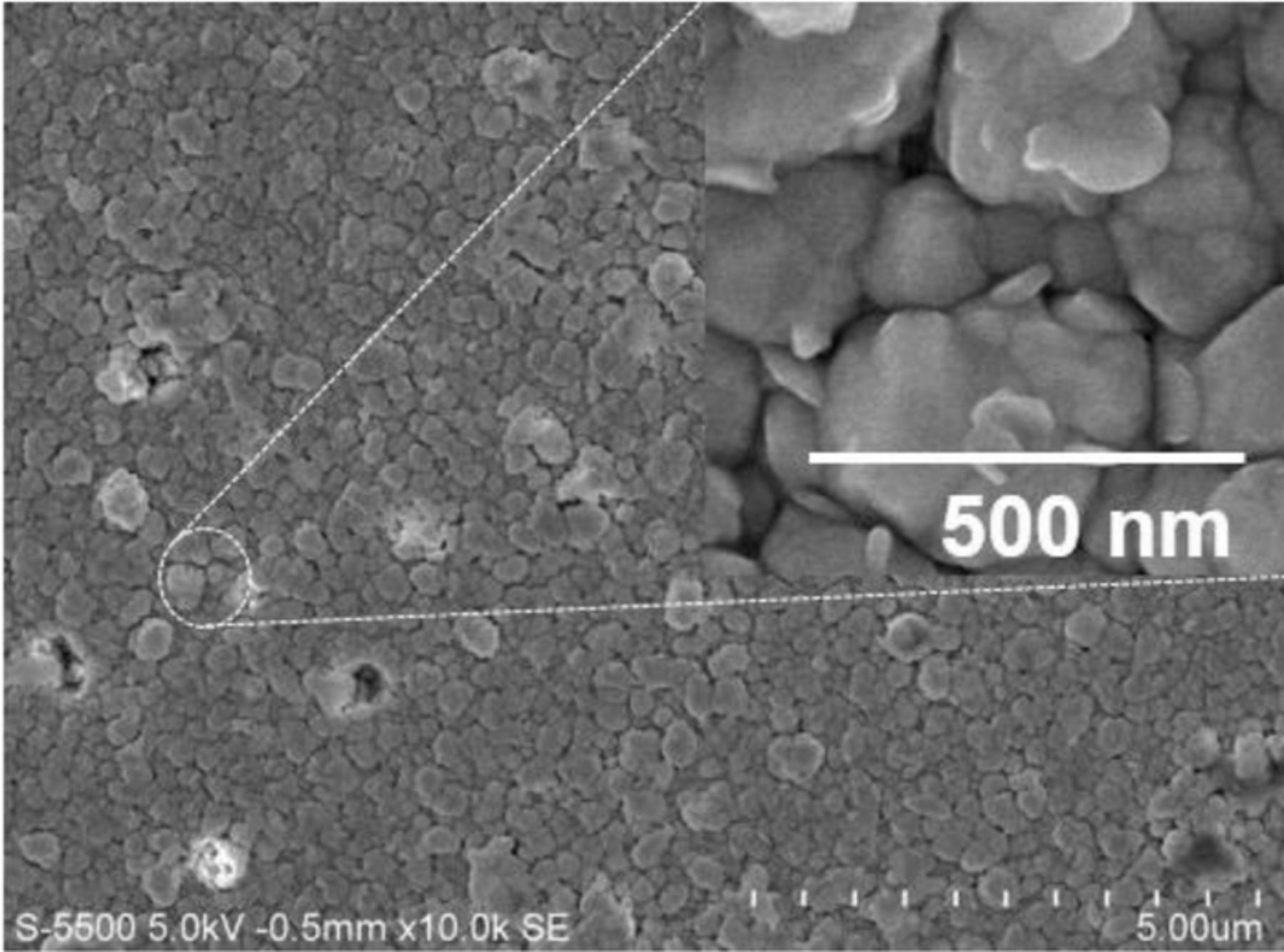
Figure 3. SEM micrograph showing the surface morphology of CZTS thin film; inset shows the magnified SEM image of the area enclosed by the circle.
The morphological and structural details of the CZTS film were further studied using STEM technique and the results are presented in the Fig. 4. Fig. 4a is the HAADF image showing clusters of different crystals fused together. Parts of few individual crystals with well-defined tetragonal feature are clearly seen. The image at higher magnification (Fig. 4b) shows well defined crystalline planes of CZTS. The fringe spacing of 0.312 nm matches well with the inter-planar distance of (112) lattice plane of kesterite CZTS (JCPDS #26 0575). The fast Fourier Transform pattern (FFT) obtained from the image (inset of Fig. 4b) also confirms the kesterite structure of CZTS as indicated by the diffraction spots corresponding to (112) and (200) planes.
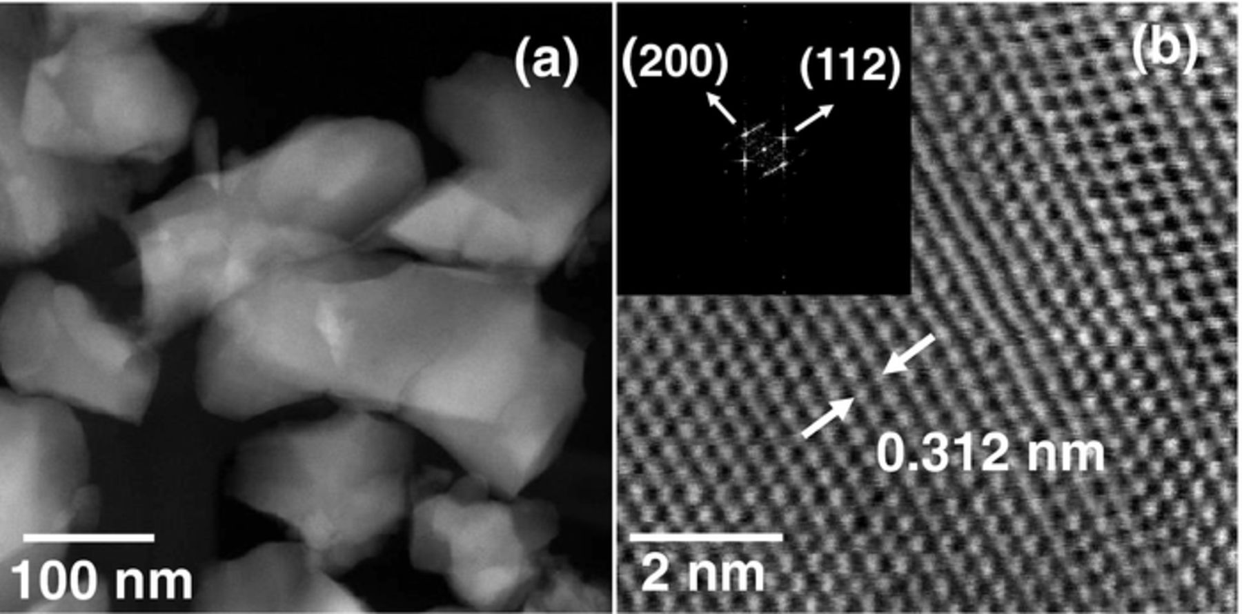
Figure 4. STEM images of phase-pure CZTS : (a) HAADF image showing the formation of grains, (b) High-resolution TEM image of the film showing well defined crystalline planes. Inset shows the fast Fourier transform pattern of CZTS crystals.
The XPS spectra were analyzed for the CZTS films in order to investigate the oxidation states of the constituent elements and the surface composition. Fig. 5a–5d represents the binding energies obtained from the high resolution core level spectra regions of Cu, Zn, Sn and S. XPS data curves are shown with the de-convoluted fitting curve after adjusting to theoretical curves. Binding energies (BE) of all the experimental peaks were corrected using C1s energy at 284.6 eV in addition to the charge compensation by the flood gun associated with the spectrometer. The Cu 2p, Zn 2p, Sn 3d and S2p were analyzed. The peaks were de-convoluted using Shirley type background calculation and peak fitting by Gaussian-Lorentzian sum function as shown in the figure. The spin orbit coupled doublets of Cu 2p core levels are observed at the binding energies of 952 eV and 932.2 eV, marked as Cu 2p1/2 and 2p3/2 (Fig. 5a). The separation of 2p doublet by 19.8 eV, is indicative of the presence of Cu as Cu (I). The satellite peak of Cu 2p3/2 which is characteristic of Cu2+ is not present, indicating the absence of any Cu2+. The resolved peaks at binding energies of 493.95 and 485.55 eV in Fig. 5b correspond to Sn 3d3/2 and Sn 3d5/2, respectively. A peak separation of 8.4 eV between the 3d5/2 and Sn 3d3/2 indicates the presence of Sn4+. The Sn 3d3/2 peak is overlapped with Zn LM2 auger line of Zn. The peaks with BE of 1044.4 eV and 1021.4 eV (Fig. 5c) are due to the Zn2p core level corresponding to 2p1/2 and 2p3/2 respectively. The peak separation is 23.03 eV, which can be attributed to Zn2+.36–38 The sulfur 2p core level exhibits two peaks, 2p3/2 and 2p1/2 with binding energies at 161.17 and 162.3 eV (Fig. 5d) with a doublet separation of 1.13 eV, which coincides with the S in metal sulfides. The XPS analysis confirms that Cu, Sn, Zn, and S exist as Cu+ Sn4+, Zn2+ and S2− respectively in our sample. These are the expected oxidation states of these elements in CZTS.
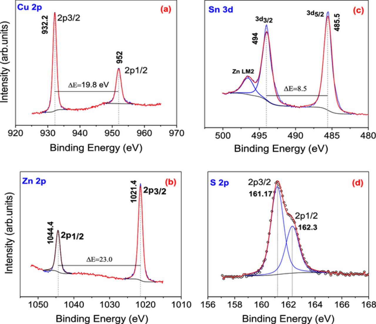
Figure 5. High resolution core level spectra of (a) Cu2p, (b) Zn2p, (c) Sn3d, and (d) S2p in CZTS film.
Optical and electrical properties
The optical transmittance T (%) and specular reflectance R (%) spectra of the CZTS thin films are shown in the inset of the Fig. 6. The optical absorption coefficient (α) at different wavelengths was calculated using the formula:
![Equation ([1])](https://content.cld.iop.org/journals/2162-8777/4/3/P91/revision1/jss_4_3_P91eqn1.jpg)
where d is the thickness of the film, Tcorr is the corrected transmittance data taking into account the reflection loss at the air-film interface;
![Equation ([2])](https://content.cld.iop.org/journals/2162-8777/4/3/P91/revision1/jss_4_3_P91eqn2.jpg)
In this case T and R are the transmittance and reflectance obtained at each wavelength.
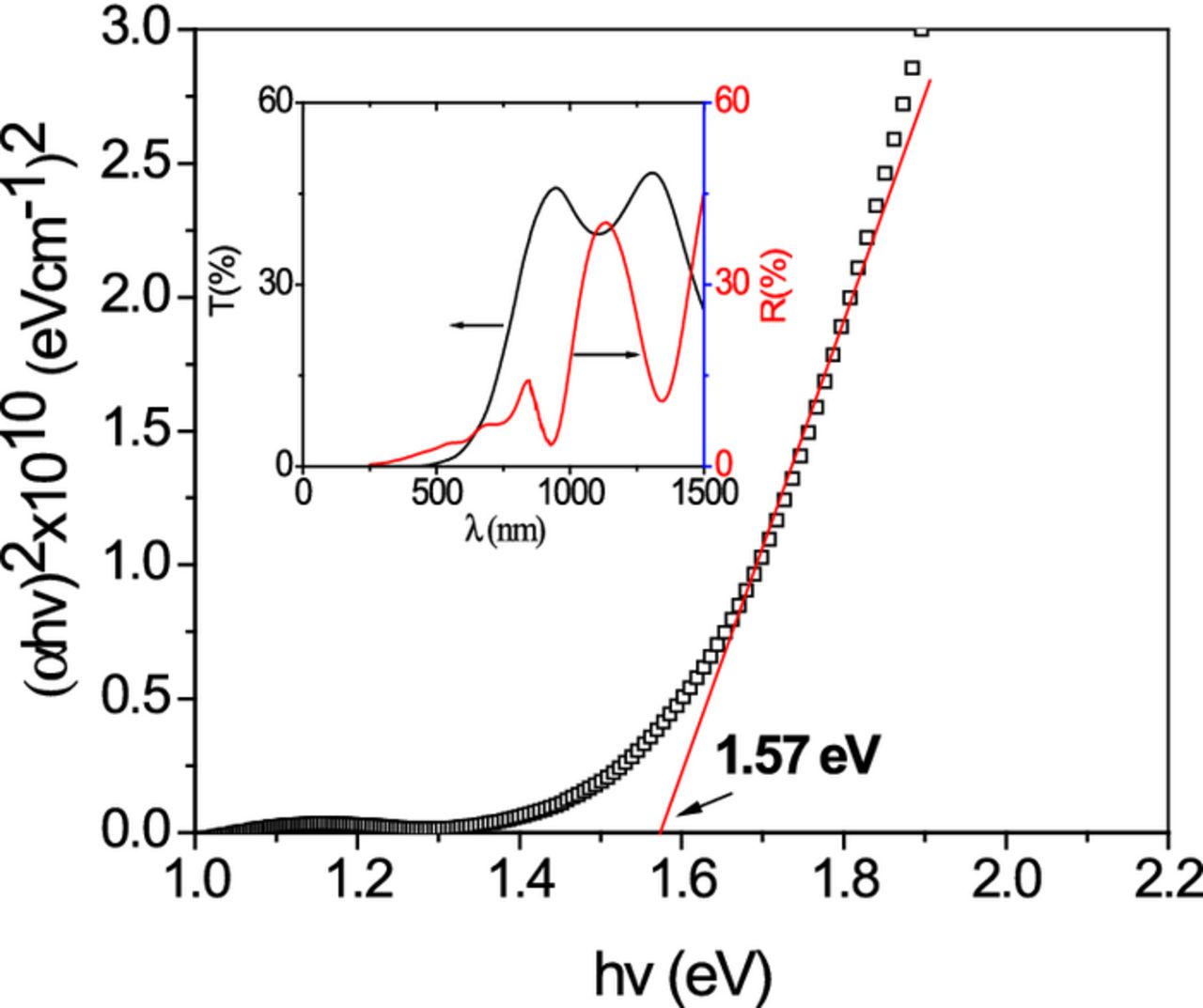
Figure 6. The plot of (αhν)2 vs. (hν), the linear portion in the plot is used to determine the bandgap of the material. Inset shows optical transmittance (T) and specular reflectance (R) of the CZTS thin film.
In semiconductors α varies with hv according to the relation:39
![Equation ([3])](https://content.cld.iop.org/journals/2162-8777/4/3/P91/revision1/jss_4_3_P91eqn3.jpg)
where A is a constant, Eg is the bandgap, hv is the photon energy. In this equation the value of n depends on the nature of electronic transitions; n is 1/2 and 3/2 for direct allowed and direct forbidden transitions, respectively; and n is 2 and 3 respectively for indirect allowed and forbidden transitions. The (αhν)2 vs hv plot is shown in Fig. 6 and the bandgap value is estimated by extrapolating the straight line fit of the curve to the energy axis. In the case of our films the estimated Eg was 1.59 eV which is close to the reported values for direct transition.40
Photocurrent response of the CZTS film is shown in Fig. 7. The measurement was performed on the film sandwiched between the TCO substrate and a carbon electrode; the electrical contacts were taken from TCO and carbon electrode, while the film was illuminated from the TCO side. Before measurement the sample was kept in the dark for about an hour to stabilize the current under a fixed bias of 0.1 V, which was maintained throughout the measurement. The absorption of light can result in an increase in the sample temperature which can lead to the thermal generation of charge carriers in the sample. However, the sudden surge in current observed at the early stage of the illumination can be considered as that due to the photogeneration of charge carriers. The current was recorded at regular intervals, in the following sequence 5s in dark, 5s in light and again 10 s in dark. The conductivity in dark of the films was in the range of 2.7 × 10⁻⁶ Ω−1cm−1.
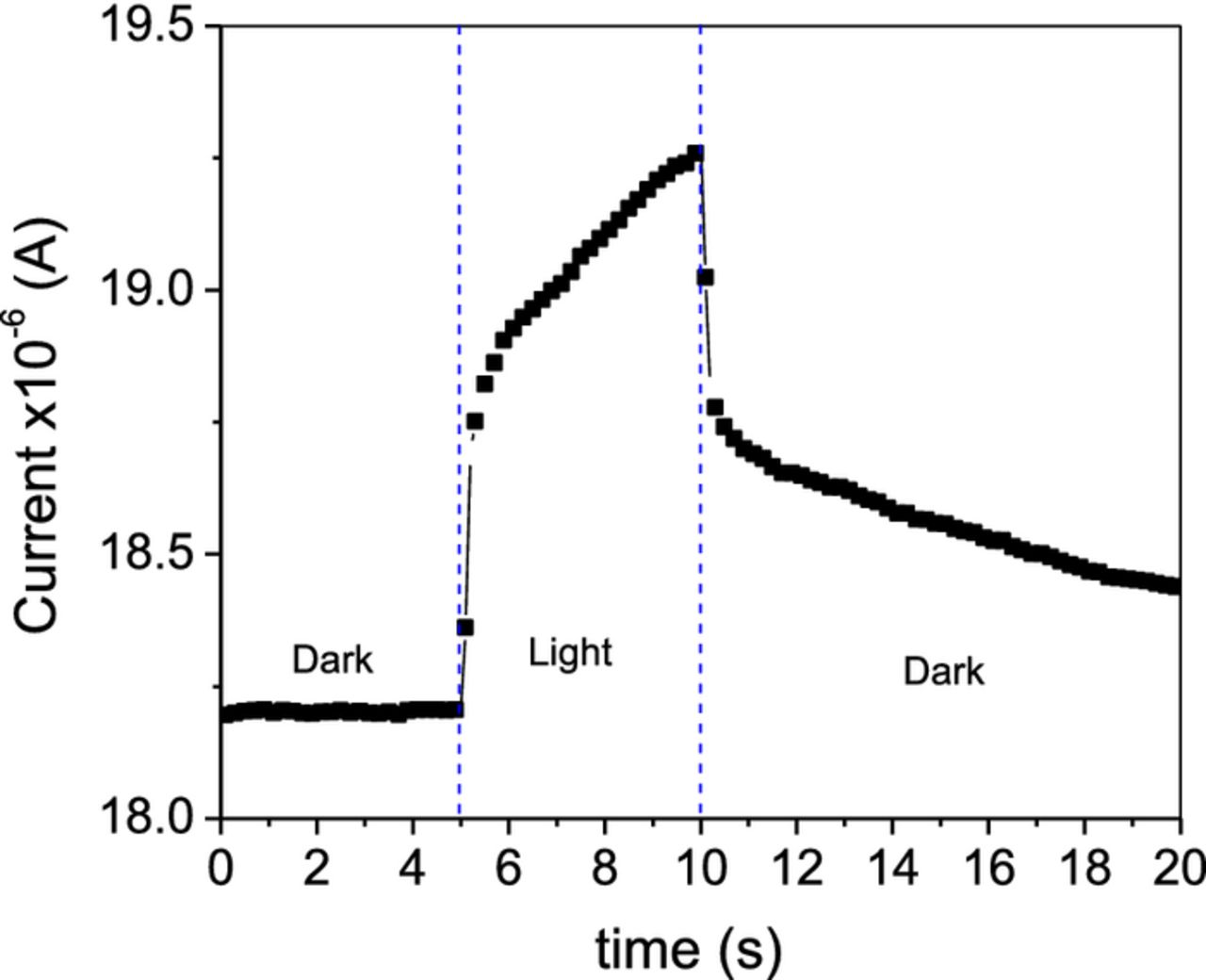
Figure 7. Photocurrent response of CZTS thin films developed by the thermal treatment of SnS/Cu/ZnS stack at 550°C in N2/S atmosphere for 30 min.
In a typical semiconductor with charge trapping centers in the bandgap, the photocurrent response follows a slow rising edge upon illumination and a transient decay under dark after cutting the illumination. The slow rise of the photocurrent upon illumination indicates trapping and the transient current in dark after illumination is due to de-trapping of the charge. Both the features are interrelated and can be interpreted as due to the presence of trap states in the bandgap of the film. However, the thermal generation of carriers can interfere with the rising (light on, heating effect) and decaying (light off, cooling with time) edge of the photocurrent, introducing certain ambiguities in the interpretation of the photoresponse. The presence of trapping states can be probed by monitoring the thermally stimulated current under dark condition.
The energetic positions of the bandgap states with respect to the band edges can be determined from the dependence of current under dark on temperature at a constant applied potential according to the equation;41
![Equation ([4])](https://content.cld.iop.org/journals/2162-8777/4/3/P91/revision1/jss_4_3_P91eqn4.jpg)
Where A is a constant, Ea is the activation energy of the trap, T is the temperature, and kB is the Boltzmann constant. The Ea can be calculated from the slope of the linear portion of the plot ln (I) vs. 1/T (Fig. 8). The graph clearly shows three regions with good fit to Eq. 4, indicating that the current transport in the film can be controlled by three trap states with energies 82, 18, and 8.2 meV. The measured activation energies are in the range of relative energetic positions of the bandgap states reported in literature.42,43 Hones et al. assigned a level with energy 5 ± 3 meV to donors below the conduction band edge, and another level with energy 10 ± 5 meV to acceptors above valance band edge.42 Grossberg et al. using the PL studies identified a band at 87 ± 15 meV, which is assigned to a donor level relatively deep in the bandgap.43

Figure 8. Current vs. 1/T plot of the CZTS films; in this measurement the CZTS film was sandwiched between TCO substrate and carbon paint electrode. Both TCO and carbon paint served as electrical contacts.
Fig. 9 shows the results of the PEC measurement for the CZTS thin film. The measurement was carried out under chopped light illumination with linearly increasing bias (0.1 to -1V vs. SCE). Under illumination, the cathodic biasing (–ve bias) showed an increase in the current (light ON) whereas anodic bias (+ve bias or decreasing negative bias) showed no difference in the current. The observed increase in current under light pulse during the cathodic scan is due to the enhancement of the reduction reaction under illumination at the semiconductor-electrolyte interface. This indicates that the charge carriers injected into the electrolyte are electrons,44 confirming that the material is p-type. The schematic of the proposed band bending at the semiconductor/electrolyte interface and the flow direction of charge are shown in inset of Fig. 9.
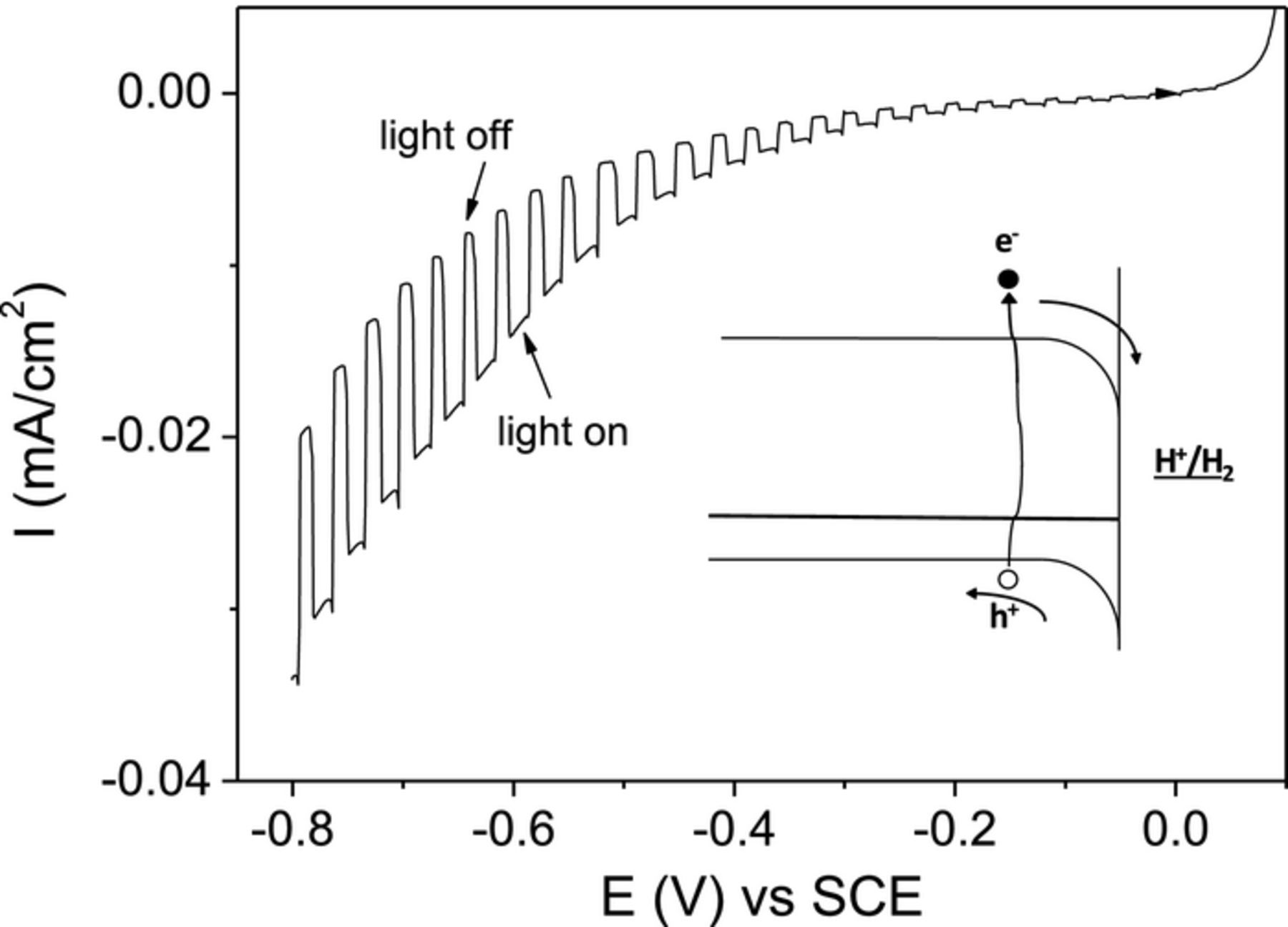
Figure 9. PEC measurements of CZTS films under chopped light illumination with bias of 0.1V to -1V vs SCE. The inset shows the proposed band diagram at the CZTS/electrolyte interface.
Conclusions
In this work we demonstrated the development of phase-pure, polycrystalline thin films of Cu2ZnSnS4 by the thermal treatments of SnS/Cu/ZnS stack in nitrogen/sulfur atmosphere. The transformation from binary-ternary phase to pure kesterite quaternary phase was studied using different experimental tools. The phase purity was confirmed by the observation of all the characteristic Raman modes. The lattice parameters of the material was estimated as a = 5.426 Å, and c = 10.856 Å, which is in agreement with the literature for Kesterite CZTS. The average crystalline size was 18 nm. The tetragonal structure determined by XRD was confirmed with the TEM analysis and the estimated interplanar distance of 0.312 nm match well with the (112) plane of kesterite. The XPS analysis confirmed that Cu, Sn, Zn and S existed as Cu+ Sn4+, Zn2+ and S2− in the sample respectively, further supporting phase-pure nature of the CZTS film formed. The band to band transition is direct and the bandgap was 1.59 eV. The films were photosensitive, and the conductivity in dark was 2.7 × 10⁻⁶ ohm−1 cm−1. The post-deposition thermal processing developed in this work identifies the experimental conditions to obtain phase-pure CZTS film with adequate structural and opto-electronic properties for applications in solar cells.
Acknowledgments
The authors thank Maria Luisa Ramón for the XRD measurements, O. Gomez Daza and José Campos Alvarez for general assistance in the chemical laboratory, Rogelio Moran Elvira for taking SEM images. The authors are thankful to Bindu Krishnan, Facultad de Ingeniería Mecánica y Eléctrica, Universidad Autónoma de Nuevo León, México for XPS analysis. This work at IER-UNAM is part of the projects CeMIE-Sol 207450/P26, and CONACyT 129169. The thermal processing performed in this paper has been benefited with the project PAPIIT IN-113214.