
Abstract
Electrical properties, deep trap spectra, microcathodoluminescence (MCL) and photoluminescence (PL) spectra of bulk semi-insulating Fe doped β-Ga2O3 crystals with ohmic and Schottky contacts were studied. The Fermi level in these crystals is pinned by the Fe acceptor level near Ec-0.8 eV. This level is also dominant in high-temperature admittance spectra and in photo-induced current transient spectroscopy (PICTS) and determines the space charge region width in Schottky diodes. The concentration of the Fe acceptors filled with electrons is (1.3–1.5) × 1017 cm−3 from high-temperature/low-frequency capacitance-voltage C-V profiling and is considerably lower than the Fe concentration introduced by doping, suggesting that a considerable portion of Fe acceptors are not filled with electrons. This is important when considering the possible role of Fe centers in charge trapping in transistors. MCL and PL spectra measurements also revealed the presence of sharp lines near 1.8 eV corresponding to the 4T1→6A1 intracenter transition in Fe3+. Additional deep centers observed in photocurrent spectra had optical ionization thresholds near 1.5 eV and 2.3 eV.
Export citation and abstract BibTeX RIS

This is an open access article distributed under the terms of the Creative Commons Attribution Non-Commercial No Derivatives 4.0 License (CC BY-NC-ND, http://creativecommons.org/licenses/by-nc-nd/4.0/), which permits non-commercial reuse, distribution, and reproduction in any medium, provided the original work is not changed in any way and is properly cited. For permission for commercial reuse, please email: oa@electrochem.org.
The properties of bulk semi-insulating (SI) β-Ga2O3 crystals compensated with Fe arise great interest because these crystals are used as substrates and buffer layers in emerging high-power field effect transistors (FETs) based on b-Ga2O3 and promising serious advantages over the more established GaN-based or SiC-based FETs due to about 3 times higher electrical breakdown field with similar value of electrons saturation current (see e.g.).1–3 Additional bonus with β-Ga2O3 is provided by the existence of high crystalline quality bulk crystals that can be prepared by relatively cheap melt-growth techniques, such as Czochralski, edge-defined film fed growth (EFG) or Bridgman methods, allowing to obtain n-type material with doping in a very wide range by using Sn, Si, Ge dopants, and semi-insulating (SI) material by using Fe doping or Mg doping.2,5 High-quality epitaxial films can be grown by halide vapor phase epitaxy (HVPE), metallorganic chemical vapor epitaxy (MOCVD), molecular beam epitaxy MBE or pulsed laser deposition.1–3 Heterojunctions of (AlxGa1-x)2O3/Ga2O3 can be grown with reasonably high quality by MOCVD for a wide range of Al compositions allowing to vary the bandgap of (AlxGa1-x)2O3 in a wide range of 4.7–5.4 eV making it possible to fabricate high electron mobility transistors (HEMTs).6,7 As a result FETs, HEMTs based on Ga2O3 that show very promising performance have been demonstrated (see e.g.).4,8,9 Currently SI-Ga2O3 substrates grown by EFG and compensated with Fe are commercially available from Tamura Corp. (Japan).10 Compensation is provided by Fe acceptors with the Fe3+/Fe2+ charge transfer state located near Ec-0.75 eV as determined by deep levels transient spectroscopy (DLTS) measurements performed on HVPE films with different concentrations of Fe (as measured by secondary ion mass spectrometry (SIMS)).10 For bulk SI-Ga2O3(Fe) crystals the Fermi level pinning position was found to be close to Ec-0.8 eV from resistivity versus temperature measurements11 and near Ec-(0.75–0.8) eV from low-frequency/high-temperature admittance spectroscopy (AS) experiments.12 These estimates are in reasonable agreement with theoretical predictions based on the density functional theory (DFT).10 Luminescent properties of Fe in Ga2O3 have been studied only cursorily and suggested the presence of a wide UV band near ∼400 nm common for most Ga2O3 crystals grown by various techniques (see review and multiple references to original papers in Ref. 2. Sharp photoluminescence (PL) lines in the near-IR spectral region and related to intracenter transitions between the excited states of the Fe3+ state are expected to exist for Ga2O3(Fe) crystals as for many other III-V and II-VI compounds,13 but have not been reported so far.
In what follows we present our studies of the position of the charge transfer Fe3+/Fe2+ level position and its compensation ratio, the spectra of other deep levels present in the material, microcathodoluminescence (MCL) and photoluminescence (PL) spectra of bulk β-Ga2O3(Fe) crystals grown by EFG. We show that Fe acceptors produce by far the most prominent deep center in the bandgap, with other deep traps giving rise to levels near ∼Ec-1.5 eV and Ec-2.3 eV, that the Fe3+ neutral states that can capture electrons during the HEMTs operation and cause current collapse as in III-N HEMTs14 are fairly abundant, and that MCL/PL spectra of such crystals are dominated by wide Gaussian defect bands peaked at 3.09 eV and 3.36 eV, by two sharp lines at 1.78 eV and 1.8 eV that we attribute to intracenter 4T1→6A1 transition in Fe3+, and by a wide defect band peaked near 1.46 eV. The latter two transitions are reported for the first time up to the authors' knowledge.
Experimental
The bulk β-Ga2O3 crystals doped with Fe were acquired from Tamura Corp. Japan. They were grown by EFG method, the samples orientation was (010), the dimensions were 10 mm × 15 mm, with thickness of 600 μm. Full-area back ohmic contact and two front ohmic contact stripes with area 7 mm × 2mm were prepared by E-beam evaporation of Ti/Au (20 nm/50 nm) on the surface subjected to Ar plasma treatment with subsequent 470°C annealing in flowing N2. Circular Ni Schottky diodes (thickness 30 nm, diameter 1.25 mm) were prepared on the front surface by E-beam evaporation through a shadow mask (the surface not subjected to plasma treatment).
Characterization involved current-voltage (I-V) measurements between the top and back ohmic contacts, I-V measurements between the top Schottky diodes and the back ohmic contact, current versus temperature (I-T) measurements at fixed applied voltage, low frequency capacitance versus voltage (C-V) measurements at high temperatures and admittance spectra (AS) measurements. These experiments were performed in the dark and under illumination with high-power light emitting diodes (LEDs) with wavelengths ranging from 940 nm to 365 nm and optical output power close to 250 mW. Deep traps spectra were assessed by photoinduced current transient spectroscopy (PICTS)15 with optical excitation with high-power LED with the wavelength of 365 nm. The temperature measurements were performed over the 280–470K temperature range using a hot stage.
PICTS spectra were measured on Ni Schottky diodes. High-power (250 mW) 365 nm (photon energy 3.4 eV) LED was used for light excitation pulses. The signal was processed as the difference between the transient current I(t) values measured at time (t) windows t1 and t2 after the end of the light pulse, ΔI = I(t1)-I(t2), by building the temperature dependence of ΔI for different time windows. ΔI in PICTS includes the temperature dependence of the product μτ (mobility μ and lifetime τ of the charge carriers whose detrapping is monitored in PICTS). To compensate for this additional temperature dependence, the PICTS signal ΔI is often divided by the photocurrent at the same temperature Iph that is in turn proportional to μτ.15 The peak in the signal corresponds to the emission rate of electrons or holes en(p) at the peak temperature TM equal to to t1, en(p) = t1, while the amplitude of the peak is proportional to the concentration of the trap giving rise to the peak. However, with ΔI not normalized to photocurrent there appears additional temperature dependence coming from the temperature dependence of μτ. Thus, building the Arrhenius plot of ln(1/(t12TM2)) versus 1000/TM allows determination of the activation energy from the slope and the capture cross section from the pre-exponential factor, while comparing the plots built for ΔI(T) and ΔI(T)/Iph(T) allows to roughly determine the temperature dependence of μτ. The magnitude of the ΔI/Iph peak is proportional to the concentration of respective traps and allows to compare relative abundances of the traps producing peaks in PICTS spectra.15 Experimental setups for I-V, I-T, C-V, admittance spectra and PICTS measurements are described elsewhere.16,17
The luminescence spectra were obtained by microcathodoluminescence (MCL) in the scanning electron microscope (SEM) and by photoluminescence (PL) spectra measurements. The MCL measurements were carried out from 80 to 300 K in a JSM 6490 scanning electron microscope (JEOL, Japan) equipped with a MonoCL3 system (Gatan, England). A Hamamatsu (Japan) photomultiplier was used as a detector. In most experiments, a probing SEM beam current of 1 nA was used and the accelerating voltage for the probing beam was varied from 10 to 30 kV. The samples were semi-insulating, therefore the temperature decrease led to the noise increase due to the sample's charging. For photoluminescence measurements, a He-Cd laser at 325 nm and pump power of 5 mW/mm2 was used. A FEU-62 photomultiplier was used as a photon detector. Measurements were carried out at temperatures of 4.2, 10, 100, 150, and 300 K.
Results and Discussion
Fermi level pinning position, relation to fe acceptor level, and compensation ratio of fe acceptors
Measurements between the top and back ohmic contacts showed that the contacts were reasonably ohmic and the temperature dependence of the current at fixed high voltage (50V) showed activation energy of 0.85 eV, which should be close to the depth of the trap level pinning the Fermi level. For Schottky diodes, rectification appeared starting at 350K- at lower temperatures the high resistance of the quasi-neutral region overpowered the impact of the Schottky barrier height. For high temperatures, the rectification pointed to the prevalence of n-type conductivity (Fig. 1a). The activation energy for the forward current of Schottky diodes measured at high forward voltage of 50V was 0.85 eV, close to the activation energy measured with ohmic contacts. Illumination with high-power 365 nm LED increased the reverse current. The open-circuit voltage was positive, indicating that the sample was high-resistivity n-type (Fig. 1b. The spectral dependence of reverse photocurrent at −10V is shown in Fig. 1c.
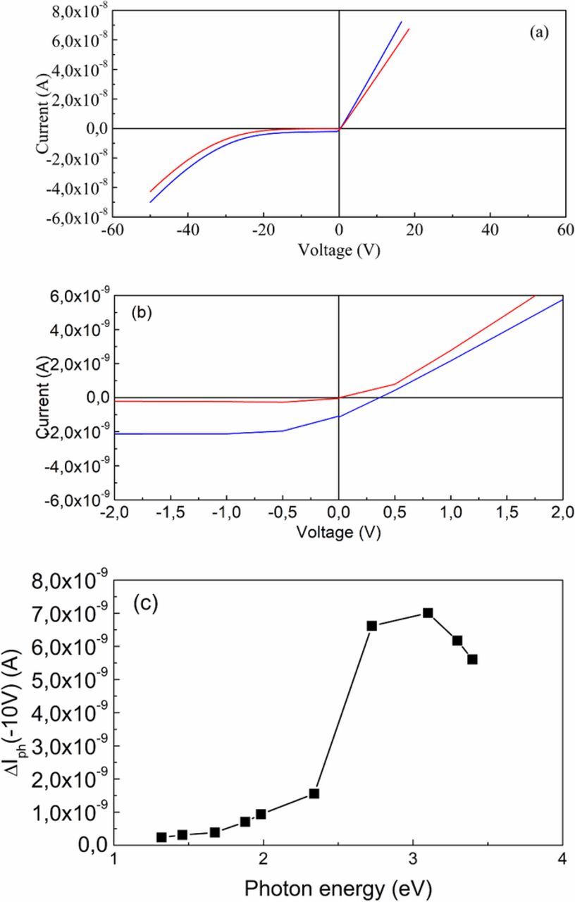
Figure 1. (Color online). (a) I-V characteristics of a Schottky diode measured at 400K in the dark (red line) and under illumination with high-power 365 nm LED (blue line); (b) blow-up of the near-0V dark and light I-V characteristic in Fig. 1(a) demonstrating positive open-circuit voltage under illumination, indicative of n-type conductivity; (c) photocurrent at −10V, ΔIph(−10V), as a function of photon energy (the dark current is subtracted).
At temperatures >350K, the series resistance of the Schottky diodes became such that it allowed measurements of capacitance dependence on voltage and of admittance spectra. Fig. 2a shows capacitance versus frequency C-f characteristics of two Schottky diodes measured at −2V at 460K. These characteristics show almost a plateau in capacitance for frequencies up to ∼1 kHz and at these low frequencies meaningful C-V profiling could be attempted. Fig. 2b presents the dark 1/C2 versus voltage (V) plots measured in the dark and under illumination with 365 nm LED at 460K. The plots are linear at low reverse voltages, showing slopes corresponding to the concentrations of deep centers filled with electrons and pinning the Fermi level (the change of the space charge width of the diodes with changing applied bias is driven by the change in electron occupation of these centers). The respective concentrations calculated from the slopes at low reverse voltage were 1.4 × 1017 cm−3 for one diode in Fig. 2b and 1.8 × 1017 cm−3 for the other, with the voltage cutoff 1.3–1.5 V. The diodes showed photocapacitance when excited with high-power 365 nm LEDs. Fig. 2c shows the concentration profiles of the charged centers computed from the data in Fig. 2b. The dark profiles are flat whereas the profiles measured under illumination with 365 nm LED (photon energy 3.4 eV) show that the near-surface regions of the diodes were enriched with the deep centers excited by the below-bandgap illumination.
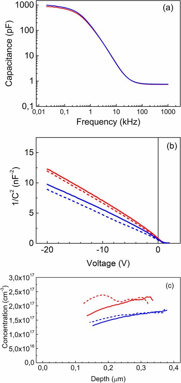
Figure 2. (Color online) (a) C-f curves for two Schottky diodes measured at 460 K and −2V; (b) C-V characteristics measured at 130 Hz on these two diodes in the dark (solid lines) and under illumination with 365 nm LED (dashed lines); (c) concentration profiles calculated from C-V characteristics in Fig. 2(b.)
The evolution of the temperature dependence of capacitance and AC conductance G measured at different low frequencies (f) display well defined steps in capacitance and corresponding peaks in conductance, as illustrated by Figs. 3a, 3b (the conductance in Fig. 3b is divided by the angular frequency ω = 2πf, as usual in presenting the conductance peaks in admittance spectra.18 The Arrhenius plots of Ln(1/(τTM2)) versus 1000/TM obtained from the shift of the G/ω peak/C step temperature TM with changing the measurement frequency f are shown in Fig. 3c (ω = 1/(2πf)18). The activation energy Ea determined from the slope and the electron capture cross sections obtained from the pre-exponential factor18 were Ea = 0.75–0.82 eV, σn = (2–5) × 10−15 cm2, close to the parameters of the Fe acceptors in Ga2O3.10 These traps pin the Fermi level, while the concentration measured by C-V profiling in the dark gives the number of electrons occupying the centers (the space charge region width at the given reverse voltage in high-resistivity semi-conductor is determined by the change in occupation of the deep trap that pins the Fermi level in the quasi-neutral region12,17). As the Fe concentration must be close to 1018 cm−3,18 a considerable portion of these centers remains free of electrons and can effectively participate in charge capture producing current collapse in Ga2O3 based HEMTs.14 The data presented above indicate that the Fermi level in SI β-Ga2O3(Fe) samples is pinned by centers whose energy level is very close to the level of Fe determined in DLTS measurements10 that give the parameters of the Fe acceptor with the charge transfer level Fe3+/Fe2+. The concentration of these Fe states filled by electrons, Fe2+ states, is estimated to be only ∼15% of the total Fe density, the rest of Fe existing as neutral Fe3+ states. This should have profound effects for electrons trapping in β-Ga2O3-based HEMTs and FETs with Fe doped substrates. One would expect strong capture of electrons from FET channels by Fe3+ in the buffer and consequent current collapse, as demonstrated by actual trapping studies reported for (AlxGa1-x)2O3/Ga2O3(Fe) HEMTs.20 This situation is also conducive to detection of intracenter transitions in Fe3+ by PL/MCL spectra measurements.
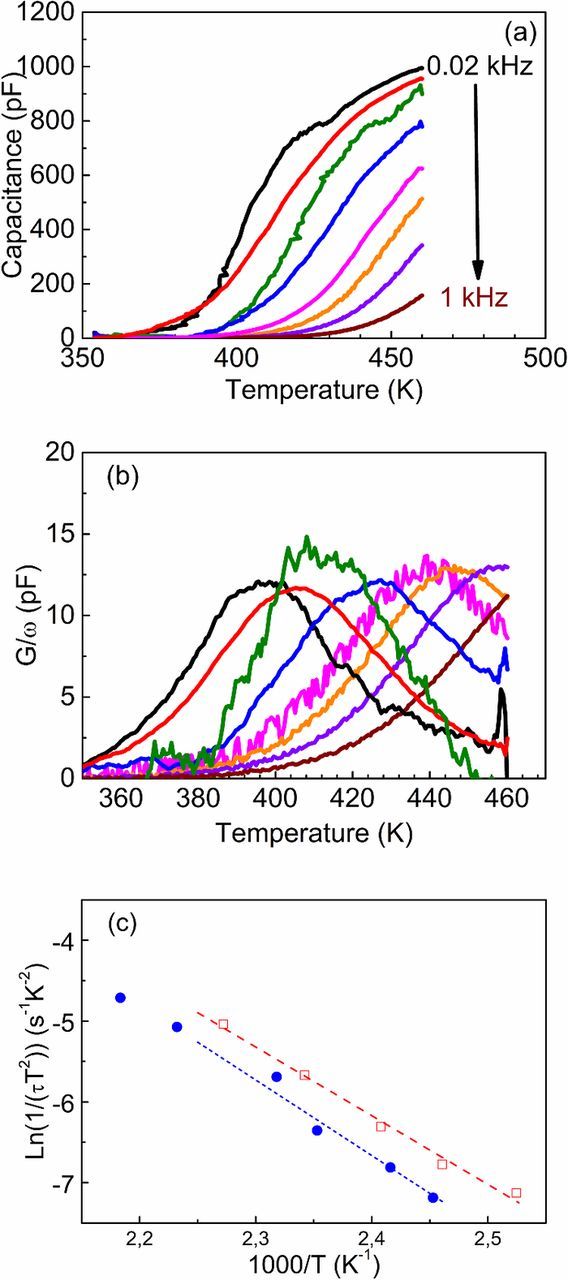
Figure 3. (Color online) (a) C-T for Schottky diodes at frequencies 0.02, 0.03, 0.05, 0.1, 0.2, 0.3, 0.5, 1 kHz; (b) conductance G divided by ω = 2πf, G/ω, for the same frequencies; (c) Arrhenius plots of 1/τT2 for the trap observed in admittance spectra, τ = 1/(2πf) for two Schottky diodes.
Deep traps spectra as determined by PICTS and photocurrent spectra
PICTS spectra measured on Schottky diodes at reverse bias of −10V, with excitation by the 365 nm high-power LED were performed. Fig. 4a shows the ΔI versus T spectra, Fig. 4b presents the spectra normalized to Iph measured simultaneously with PICTS spectra. Measurable photocurrent appeared above 330K. Both spectra showed one prominent peak. Arrhenius plots for both types of spectra are shown in Fig. 4c. The normalized ΔI/Iph spectra yielded the apparent trap activation energy of Ea = 0.8 eV with the electron capture cross section of σn = 2.7 × 10⁻¹⁶ cm2, close to the Fe level signature reported for DLTS measurements and observed in admittance spectra in Fig. 3. For the spectra not normalized by photocurrent, the apparent activation energy was 0.95 eV, yielding an activation energy for the μτ product of 0.15 eV coming predominantly from the temperature dependence of τ. PICTS results indicate that Fe acceptors are the most prominent deep centers observed in these semi-insulating β-Ga2O3 (Fe) crystals for the probed temperature range. The presence of additional deep traps could be detected by measurements of reverse photocurrent dependence on photon energy displayed in Fig. 1c. The spectrum of photocurrent is dominated by deep traps with optical ionization thresholds of 1.5 eV and 2.3 eV, both of which should be fully occupied in the dark, given the Fermi level pinning near Ec-0.8 eV (see above). The centers with optical ionization threshold near 2.3 eV are common for bulk β-Ga2O3 and for epitaxial films grown by HVPE or metallorganic chemical vapor deposition.21,22
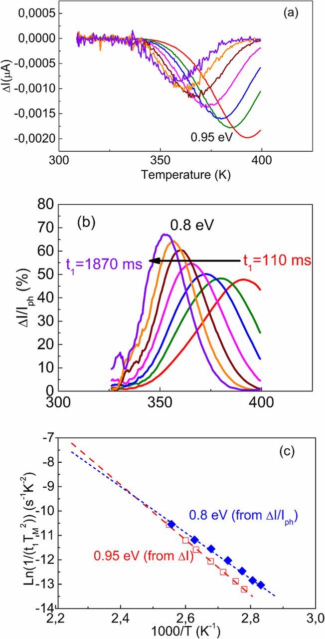
Figure 4. (Color online) (a) PICTS spectra ΔI = I(t1)-I(t2) from Schottky diodes for reverse bias −10V, excitation with 365 nm LED (pulse 5s) and with t1/t2 = 100 ms/550 ms, 220 ms/1100 ms, 330 ms/1650 ms, 550 ms/2750 ms, 880 ms/4400 ms, 1320 ms/6600 ms, 1870 ms/9350 ms; (b)PICTS spectra presented as ΔI/Iph; (c) Arrhenius plots calculated from PICTS spectra in Fig. 4(a, b).
Deeper electron traps with optical threshold near 1.5 eV and 2.3 eV are expected to produce their peaks in PICTS at much higher temperatures than used here. These traps should be fully occupied with electrons in the dark and should not be a concern for current collapse in HEMTs, but could present a problem under illumination, particularly in the case of very deep and relatively abundant traps with optical threshold of 2.3 eV (Fig. 1).
MCL and PL spectra: detected new bands and lines
The dominant feature of the MCL spectra measured at different temperatures was a broad band peaked near 386 nm. Fig. 5a shows the MCL spectra in the region of this broad band for measurements at 295K and 80K. This feature has been often reported for MCL and PL spectra measurements of variously grown β-Ga2O3 crystals23–28 and is close to the so called UV band of.23 This UV band could in our case be accurately deconvoluted into two broad Gaussian bands peaked at 3.09 eV and 3.36 eV whose positions were not measurably affected by temperature change from 80K to 295K (Fig. 5a). The slight temperature dependence of the peak positions of both bands implies that they could be due to donor-acceptor transitions. There have been multiple attempts to associate various constituents of the broad UV band with transitions involving deep oxygen donors and deep Ga acceptors,23–28 but the proposed identifications do not seem unambiguous and need further verification. In addition to the UV band discussed above our MCL spectra also showed a broad band peaked near 1.75 eV (Fig. 5b) that is most likely the second order reflection of the UV band at 386 nm. It is interesting, however, that on the high energy slope of this "parasitic" band one can observe two sharp peaks near 1.78 eV and 1.8 eV that have not been reported before and have to belong to some intracenter transitions judging by their extremely narrow width. Our MCL system does not allow to filter out the parasitic second order reflection and to study in detail these new peaks. To do that we measured PL spectra excited at various temperatures by 325 nm-wavelength (3.8 eV) laser excitation. As shown in Ref. 23 with such excitation the UV band is not excited and consequently there is no second order reflection near 750 nm. The 10 K PL spectrum measured with our He-Cd laser 3.8 eV excitation is shown in Fig. 6a. One can clearly see a very sharp line near 696 nm (1.78 eV) with two sidebands near 713 nm (1.74 eV) and 731 nm (1.7 eV), and a broad band peaked near 845 nm (1.46 eV). As far as the authors are aware neither of these features has been reported previously. The sharp line at 1.78 eV cannot be anything else then some sort of intracenter transition, most likely involving some transition metal impurity. Since it has only been detected in a heavily Fe doped sample and since Fe is by all means the most dominant deep level defect in the studied β-Ga2O3(Fe) it stands to perfect reason to associate the 1.78 eV line with intracenter transition in either the Fe2+ or Fe3+ states. From what we know about the pattern of levels in Fe ions in different III-V and II-VI compounds only transition between excited states in the Fe3+ ion produce near-IR PL bands, the Fe2+ transitions all lying in the far IR.13 The most obvious explanation of the observed 10K PL pattern is that we are dealing with the 4T1→6A1 and its phonon sidebands,13 the phonon energies being near 40 meV, close to the energy of optical phonons held responsible for the observed temperature dependence of mobility in n-Ga2O3.29 Similar PL bands in GaN, AlN lie near 1.29 eV.13 In ZnO with increased ionic contribution to bonding the energy is increased to 1.78 eV in agreement with theoretical considerations that predict the energy to increase with increased ionicity.13,30,31 In that sense Ga2O3 certainly follows suit because its bond is more ionic than in III-Nitrides.2 If the attribution above is right one expects that, with increasing temperature the sharp line at 1.78 eV should show at higher temperatures an additional high energy line due to growing occupation of the excited state of the 4T1. The relative intensity of this high energy line of the doublet should increase with temperature.13 As demonstrated by Fig. 6b this is indeed happening in our PL spectra. As the temperature increases from 10K to 50K, 100K, 150K an additional high energy line at 1.8 eV emerges and its intensity increases. We have to point out that the possibility of the second sharp line to be related to Fe occupying Ga sites in two different positions, the octahedral and the tetrahedral10 has been discarded above, firstly, because theory suggests the octahedral site to be energetically more favorable and secondly, because it is hard to understand why, with these two states of Fe, we should observe a doublet rather than a quartet. Of course, much more work including measurements of the observed levels splitting with applied uniaxial stress and magnetic field is necessary to establish the full pattern of excited states in Fe ions in β-Ga2O3. But locating the lines that are to be monitored in such experiments is the first necessary step. These studies could also have not only pure scientific interest. In GaN it has been quite convincingly demonstrated that Fe is a very efficient recombination center32 despite the fact that its charge transfer Fe3+/Fe2+ level near Ec-0.5 eV33 is far away from midgap and thus should not be particularly suitable for fast capture of both electrons and holes via multiphonon emission model.34 To explain the contradiction the energy recycling via excited states of Fe2+and Fe3+ has been invoked in Ref. 34 to achieve good agreement with experiment.
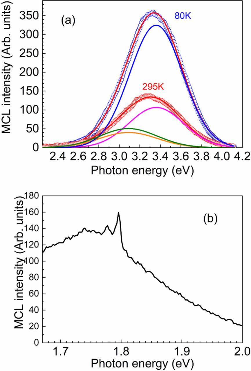
Figure 5. (Color online) (a) MCL spectra in the 2.3 eV–4.2 eV range measured at 80K (blue open circles) and 295K (red open circles); also shown are the results of two Gaussian bands fitting with peak energies 3.09 eV (olive line for 80K and orange line for 295K) and 3.36 eV (blue line for 80K and magenta line for 295K); the results of fitting are represented by solid lines connecting the experimental points; (b) sharp peaks near 1.78 eV and 1.8 eV in MCL spectra at 295K clearly visible against the backdrop of the broad peak due to second order reflection of the UV band.
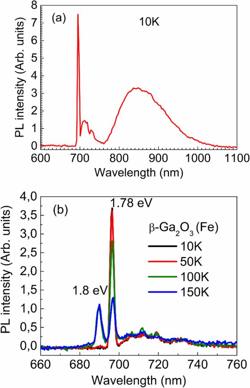
Figure 6. (Color online) (a) 10K PL spectrum measured with 325 nm laser excitation; (b)PL spectra in the region of the Fe3+ intracenter transitions at 10K, 50K, 100K, and 150K (the amplitudes of the 1.8 eV peaks similar for these temperatures while the amplitude of the 1.78 eV peak decreased at 150K compared to 100K).
The PL band peaked near 850 nm (1.46 eV) is too broad to be related to intracenter transitions. Its origin has yet to be understood. The width of the band suggests either a strong lattice relaxation of the center involved or some sort of donor-acceptor recombination, but more work is needed here.
Conclusions
The dominant feature in β-Ga2O3 doped with Fe is the Fe3+/Fe2+ charge transition acceptor level near Ec-0.8 eV. These centers pin the Fermi level and determine the temperature dependence of the dark conductivity. The concentration of the Fe acceptors filled with electrons and determining the extent of the space charge region in Schottky diodes is (1.4–1.8) × 1017 cm−3 and is lower than the concentration of Fe, judging by the correlation between the resistivity and the Fe concentration.19 This can result in trapping and current collapse in (AlxGa1-x)2O3/Ga2O3 HEMTs.20 PL and MCL spectra measurements indicate the presence of prominent sharp lines near 1.8 eV belonging to the 4T1→6A1 intracenter transitions in Fe3+.13 The energy positions of these lines is shifted to higher values than observed in nitrides13 and is close to the intracenter transitions in ZnO(Fe),32,33 because the bonding in Ga2O3 is more ionic than in nitrides. Detailed studies of the intracenter transitions in Fe doped Ga2O3, including orientation dependence, splitting in magnetic field and under uniaxial stress and temperature effects are of interest given the role of the excited states of Fe in nonradiative recombination in GaN.32–34 Other deep centers detected by photocurrent and PL spectra measurements reveal centers with optical ionization thresholds 1.5 eV and 2.3 eV. Both traps lie below the Fermi level pinning energy near Ec-0.8 eV and should not contribute to current collapse in HEMTs.
Acknowledgments
The work at NUST MISiS was supported in part by the Ministry of Education and Science of the Russian Federation in the framework of Increase Competitiveness Program of NUST (MISiS) (K2-2017-068). The work at UF was sponsored by the Department of the Defense, Defense Threat Reduction Agency, HDTRA1-17-1-011, monitored by Jacob Calkins.
ORCID
A. Y. Polyakov 0000-0001-6898-6126
N. B. Smirnov 0000-0002-4993-0175
A. V. Chernykh 0000-0003-2450-8872
S. J. Pearton 0000-0001-6498-1256