
Abstract
Thin aluminum foils were surface roughened by laser ablation in high vacuum conditions. Their performance as current collectors for carbon-based supercapacitors were evaluated by impedance spectroscopy, cyclic voltammetry and galvanostatic cycling, and compared with those of gold plates, flat aluminum foils and commercially available carbon-coated aluminum foils (Z-flo). The results revealed that the laser surface treatment significantly enhances the electronic contact between the current collector and the active materials layers. The benefits in interface enhancement are comparable to those of a carbon coating. High power performances were reached thanks to a significantly decreased internal resistance. Long-term cycling performance revealed a slight but continuous capacity fading for supercapacitor cells having laser-treated current collectors, which was caused by the progressive growth of a surface aluminum oxide layer on the current collector. Cells assembled with carbon-coated collectors did not display the same fading thanks to the protection provided by the interfacial carbon layer. This work demonstrates that laser ablation in vacuum is a promising technique for the preparation supercapacitor current collectors with surface oxide-free and controllable surface microstructures toward specific active materials.
Export citation and abstract BibTeX RIS
Supercapacitors are among the most promising energy storage devices, due to their high power density, high efficiency, short recharging times, low temperature operation, as well as long shelf and cycle life.1 They are particularly well suited for electric and hybrid vehicles to provide acceleration power and braking energy recovery.2 Combining supercapacitors and batteries can significantly improve batteries lifetime in electric vehicle applications in which the vehicle power sources are subject to high current pulses in both charge and discharge.3,4 Supercapacitors store energy using either ion adsorption (electrochemical double-layer capacitors) or fast surface redox reactions (pseudo-capacitors). For power devices like supercapacitors, interfaces play a significant role in the performances and are often the cause of their limitations. The most critical interface in a supercapacitor is the one between the current collector and the active layer. The current collector globally used for supercapacitors is aluminum, thanks to its light weight, low cost and high electrical conductivity.5 However, pure aluminum reacts readily with oxygen in air, creating a thin aluminum oxide layer next to the metal surface, with a typical thickness of about 2–3 nanometers, growing to ∼5 nm after a few days, reaching a complete passivation of the surface.6 This oxide layer is a natural electrically passivation barrier which stabilizes the surface, protecting it from further reactions with the environment. When the passivation layer is thin enough, electrons can tunnel through it. But when exposed to oxidative environments and conditions, such as the presence of aqueous electrolytes, impurities in organic electrolytes, high voltages, or combinations of those factors, the insulating oxide layer may continue to grow to thicknesses which do not let electrons tunnel efficiently. This phenomenon can considerably decrease the power output and performance of supercapacitors.
One of the strategies to overcome this challenge is to reduce the interface impedance between electrode active materials and current collectors and maintain this value low during the life-span of the supercapacitors. Chemical and electrochemical etching can be used to remove the oxide layer of aluminum current collectors. However, etch residual, reactants, and byproducts from chemical etching process can be trapped inside the porous surface of the chemically etched current collector and become reactive toward the active materials and electrolyte as well as toward the current collector itself in the presence of electrolyte. Contamination issues with chemical etching could induce degradation of active materials and electrolyte as well as increase the interface resistance between the current collector and electrode active materials, and therefore are of concern for long term cyclic stability and device longevity of supercapacitors. Furthermore, some etchants, such as hydrofluoric acid, are highly toxic and may have adverse impacts on human health and the environment.
To protect etched aluminum current collectors from surface oxidation and the resultant formation of electrical insulation at the electrode active material/current collector interface, there is a need for protective coatings. The coatings need to be electrically conductive, nonreactive with active materials, and corrosion resistant in the electrochemical environment that uses either aqueous electrolytes or corrosive salts in organic electrolytes. Portet et al.7,8 used electrochemical etching to increase the surface area and remove oxides from aluminum current collectors and then deposited a conducting carbonaceous material on the etched surface by a sol–gel technique. Another approach to reduce the interface impedance between electrode active materials and current collectors is to enlarge the contact area between electrode active materials and current collectors since the ability to collect electrical charge from active materials depends on the surface area of current collectors. Many efforts have been carried out to develop methods to increase surface area of current collectors. Chang et al.9 used nanoporous nickel (Ni) substrate prepared by selective dissolution of copper (Cu) from a Ni–Cu alloy layer as current collectors for supercapacitors based on manganese oxide. The specific capacitance of the manganese oxide deposited on nanoporous Ni current collectors was 85% higher than that deposited on a flat electrode and reached 502 F g−1. Yoon et al.10 also used 3-dimensional porous nickel foam as a current collector for supercapacitor based on cobalt oxide active material. High specific capacitance values (445 F/g at 10 mV/s and 350 F/g at 200 mV/s) and excellent capacitance retention ratio (99% after 104 cycles) were found for the Co3O4/nickel foam electrode, which were attributed to the reduced interfacial resistance between nickel foam and cobalt oxide.
However, the ability of chemical etching process to control surface patterns, roughness and quality is typically limited. Etching chemicals, temperature and time are key influential factors on surface finish quality during chemical etching. Physical etching, such as plasma or ion gun etching, will also effectively remove the native oxide film, but the etching methods will not substantially increase the surface area. Therefore a need remains for producing rough surface with controlled morphology to match size and shape of electrode active material particles as well as higher surface areas than conventional chemical and physical roughening.
Laser treatment of current collectors has been scarcely reported. Yet it is an efficient method to create surface patterns and increase the surface area with a very good control, reproducibility and surface homogeneity. Y. Huang et al.5 used a coherent picosecond laser beam to treat Al current collectors and tested them in supercapacitors. They focused the laser in order to pattern the Al foil surface and create evenly spaced lines and rows. The laser treatment in their experiments resulted in hierarchical micro−nanostructures on the surface of the Al foil. The electrochemical performance of the thus prepared Al foil was examined in symmetrical activated carbon supercapacitors with an organic electrolyte. Their results suggest that the laser-treated Al foil (laser-Al) increased the capacitance of supercapacitors up to 110.1 F g−1 and improved the rate capability due to its low contact resistance with the carbonaceous electrode and high electrical conductivity derived from its larger specific surface area. However, the laser surface treatment performed by Y. Huang et al. occurred in open air atmosphere, and therefore, surface oxidation of aluminum cannot be avoided due to its high reactivity in air. Atomic percentage of oxygen on their laser surface treated Al foil was only slightly lower than pristine Al (55.39% for laser treated and 56.35% for pristine Al) as shown by XPS analysis. In this work, we report the use of laser ablation process in vacuum conditions, to roughen the surface of aluminum (Al) current collectors. Laser ablation refers to the phenomenon in which a low wavelength and short pulse (ns-fs) duration of laser beam irradiates the surface of a substrate to induce instant local vaporization of the substrate material resulting in surface modification of materials. 50 μm thick Al foils were surface-roughened by a diode pumped solid state Q-switched laser operating at 1064 nm wavelength in high vacuum, to increase the surface area and create patterns at the surface of the foil. The laser-treated (LT) foils were then evaluated as current collectors in carbon-based supercapacitors. The impedance, specific capacitance, cyclic durability, energy and power of the supercapacitors were measured and compared to supercapacitors assembled with gold plates, flat Al foils and commercially available carbon-coated foils (TC Transcontinental Z-flo), to demonstrate how the laser ablation process can enhance the interface between current collectors and the active materials layers.
Experimental
Surface treatment of Al current collectors by laser ablation
Surface treatment of Al foils by laser ablation in vacuum conditions was performed using the experimental set-up shown in Figure 1. The system includes a home-made high-vacuum stainless steel chamber with a quartz glass cover to allow a laser beam to pass through; a Spectra-PhysicsTM diode pumped solid state Q-switched laser (Model J40-BL6-106Q, operating at 1064 nm wavelength, with a power > 5.0 W, energy per pulse > 140 μJ, pulse width 6 ns and repetition rate of 1–150 kHz); an AerotechTM X-Y-Z 3-axis motion stage to which the laser was mounted; and conventional laser beam focusing optics (focusing the beam to 30 μm diameter). Aluminum foils with 50 micron thickness were mechanically mounted on a smooth ceramic support disc within the vacuum chamber. The chamber was pumped down to high vacuum level (below 5 × 10⁻⁶ Torr) using a turbo pump and a mechanical pump. The laser beam was focused onto the surface of aluminum foils by means of a focal length lens and z axis motion stage. The laser beam was scanned on the foil surface in x and y directions during the roughening process. The x, y and z axes motion of the laser beam was controlled by the Aerotech X-Y-Z 3-axis motion stage with its associated software. The x-y-z motion stage was controlled to scan the large surface of metal foils to roughen the surface over ∼100 cm2. The scan rate was about 200 mm/min, and the pulse rate was 500–10 kHz.
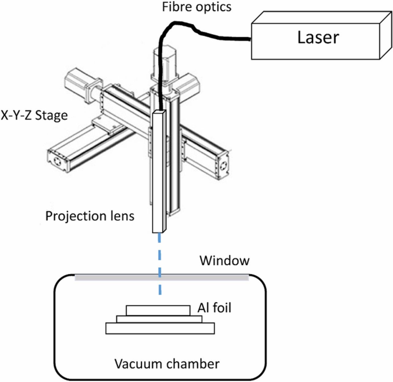
Figure 1. A schematic illustration of the experimental set-up for laser ablation of Al foils in a vacuum chamber.
Electrochemical characterization
Activated carbon-based supercapacitors were assembled for electrochemical performance testing. A dry electrode paste technology was used with PTFE as binder (as opposed to a wet technology where the active material layer is formulated as ink and then coated on the surface of the current collector). The active material layer was composed of 85 wt% RP20 (Kuraray), 10 wt% Ketjenblack EC600JD (Akzo Nobel) and 5 wt% polytetrafluoroethylene (PTFE) binder (60 wt% dispersion in water, Aldrich). Active layer pastes were calendered to a thickness of 100 ± 2 μm. They were then punched into disks with a 16 mm diameter and dried at 120°C under active vacuum for at least 48 h. They were pressed onto the current collectors using a hydraulic press. The optimal pressing conditions were found to be 10,000 lbs for 30 s at a temperature of 100°C. The electrodes (active layers and current collector) were dried for another 12 h at 120°C under active vacuum before transfer into the glove box for cell assembly.
The current collectors tested in this study included flat 50 μm thick Al foils, LT Al foils, Z-Flo Al foils (carbon-coated) and gold plates. The flat Al foils were subjected to a regeneration of the native alumina layer by dipping them into a 1M NaOH solution for 30 s (to dissolve the alumina layer), rinsing them thoroughly with water and then with acetone. The Al foils were dried at 120°C under active vacuum for 24 h. This procedure made sure that the history of the Al surface was erased and that a minimal alumina layer was present at the surface. This procedure was not carried out with LT Al foils since the laser treatment ablated the Al surface, getting rid of the former alumina layer in the process.
Supercapacitors were assembled in a glove box under argon atmosphere (O2 ≤ 0.1 ppm; H2O ≤ 0.1 ppm) using ECC-Ref cells (EL-CELL, Germany). The electrodes were assembled with two layers of a 25 μm thick microporous PTFE separator (W. L Gore) in-between and 100 μl of organic electrolyte (NEt4BF4 1M in ACN). All electrochemical characterization was performed using a Bio-Logic VMP3 multipotentiostat (France). The impedance of the supercapacitor cells was investigated using EIS (Electrochemical Impedance Spectroscopy) in their discharged state, using a 10 mV amplitude between in the frequency range 10 mHz to 0.2 MHz. The low intercept of the X-axis of Nyquist plots was used to measure the high frequency equivalent series resistance (ESR), typically related to charge transfer at the interface between the current collector and the active layer. The cells were then cycled between fully discharged and fully charged states using either cyclic voltammetry (CV) or galvanostatic cycling (GC) at different rates (scan rate in CV, current in GC) and RP20 specific capacitances were determined from these results.
Results and Discussion
SEM/EDX and optical profilometry characterization of laser roughened 50 μm thick Al current collectors
Figures 2a–2i shows the wide variety of possible surface morphologies obtained by varying the ablation parameters of the diode pumped solid state Q-switched laser, as listed in Table I. Warping and tearing of the foils was not observed, as the ablation was set to a depth of 2–20 μm for the 50 μm thick foil. The limit of the machined depth of Al foil depends on its thickness: the thinner the foil is, the smaller is the machined depth. To preserve a minimal mechanical strength is needed during the subsequent coating and cell assembly steps.
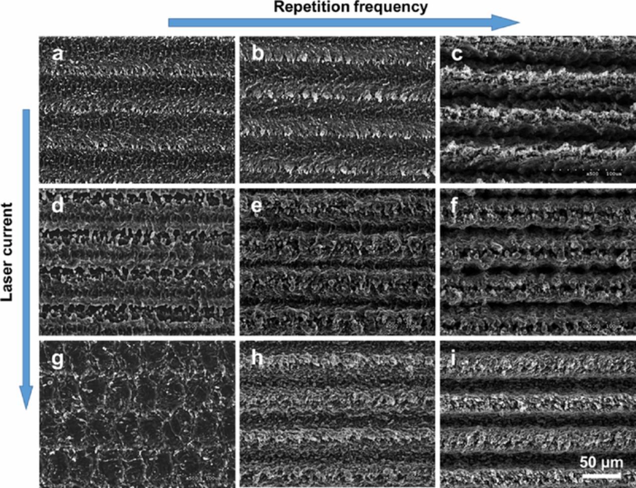
Figure 2. SEM micrographs at 500x magnification of the 50 micron thick Al foil, with 9 different sets of laser ablation parameters, showing how surface morphologies can be adjusted by the method.
Table I. Laser parameters used to produce the respective surface roughened micrographs in Figures 1a–1i.
| SEM Figure # | Diode laser drive current (A) | Repetition rate (Hz) | Power (w) | Pulse Energy (μJ) | Energy density per pulse (J/cm2) |
|---|---|---|---|---|---|
| a | 20 | 500 | 0.052 | 104 | 0.035 |
| b | 20 | 1000 | 0.101 | 101 | 0.034 |
| c | 20 | 5000 | 0.490 | 98 | 0.033 |
| d | 25 | 500 | 0.081 | 162 | 0.054 |
| e | 25 | 1000 | 0.154 | 154 | 0.051 |
| f | 25 | 5000 | 0.722 | 144 | 0.048 |
| g | 30 | 100 | 0.066 | 660 | 0.22 |
| h | 30 | 500 | 0.133 | 266 | 0.089 |
| i | 30 | 1000 | 0.210 | 219 | 0.073 |
Figure 2 clearly shows that by adjusting the laser processing parameters, various surface morphologies of Al foils can be reproducibly obtained and controlled. When using a diode laser drive current of 20 A and a repetition rate of 500 Hz (Fig. 2a), the surface was only slightly etched, and even though the surface roughness was substantially increased, the trenches created by the treatment remained very shallow. By increasing the repetition rate (Figs. 2b and 2c), deeper features were progressively created. On the other hand, it was also possible to vary the surface roughness, while mostly preserving the treatment depth, by increasing the drive current (cf. Figs. 2d and 2g). By playing with those two parameters (power and repetition rate), a variety of surface roughness and treatment depth were obtained (cf. Figures 2a to 2i).
Surface morphology of current collectors that can better match the particle size and shape of electrode active material should be used. Good matching between current collector and active materials should enhance their contact area thereafter, reducing the interface resistance. The ease of control of the surface morphology by laser ablation is one of the main advantages of this method over other surface etching methods such as chemical etching or plasma etching. Particularly, laser ablation using ultrafast lasers allows surface roughening of very thin metallic current collectors without losing the mechanical strength required for battery or supercapacitor applications.
The LT Al foil shown in Figure 2h was selected to be tested as the current collector of carbon-based supercapacitors, in a comparative investigation of the impact of various current collector surfaces on the electrochemical performances. The surface obtained with these parameters presents a good compromise between treatment depth and surface roughness. Moreover, it can nicely match the multiple particle size and distribution of the Kuraray RP20 activated carbon (D50 of 5 μm and D90 of 7.5 μm, divided into three particle distributions centered at 0.3, 2.7 and 6.2 μm, respectively; cf. Figure S1). Importantly, other morphologies may not necessarily be worse choices compared to morphology (h). Figure 3 shows SEM images of the surface (a) and cross sectional (b) views of the corresponding foil (ablation parameters listed on Table I, sample h) as well as optical profile graphs (c). The surface was analyzed using a Wyko optical profilometer along three lines: a horizontal line along a valley, a horizontal line along a ridge and a vertical line that crossed valleys and ridges. Table II lists the surface roughness parameters that were obtained from these measurements. The depth of laser roughening was given by the maximum peak height minus maximum profile depth across the ridge-valley, which is around 8.1 μm when measured along the vertical line. The root mean square roughness (root mean square of a surfaces measured across the microscopic peaks and valleys) and average roughness (the arithmetic average of surface heights measured across the microscopic peaks and valleys) are in the range of 0.40-0.49 μm along the valley and in the range of 0.70-0.88 μm along the ridge. The root mean square and average roughness are in the range of 1.62-1.85 μm across the profile ridge-valley.
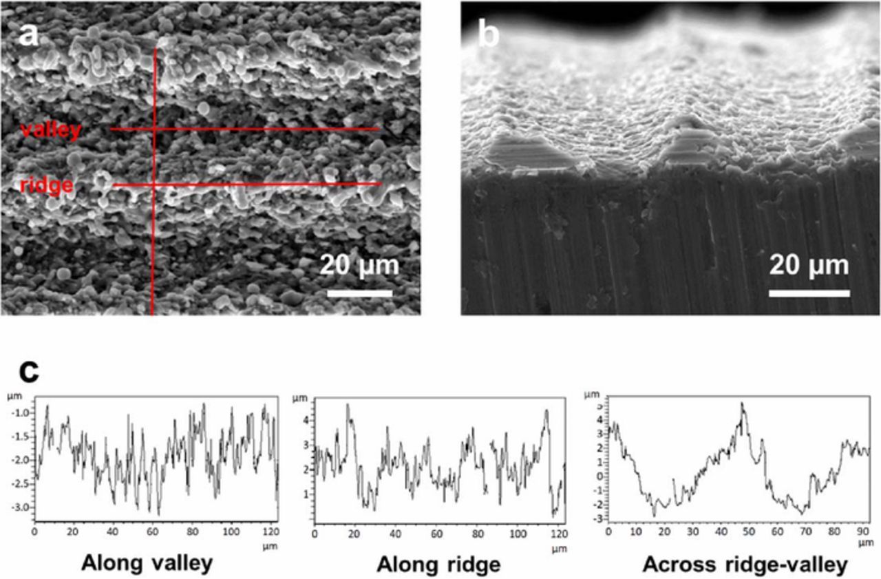
Figure 3. SEM micrographs of sample (h) from Fig. 2. (a) top view, (b) cross-sectional view. (c) Optical profilometry lines measured at the surface of sample (h) as displayed in (a). Lines in (a) are just guides for the eye, not the actual profilometry lines performed.
Table II. Surface roughness of sample h.
| Laser roughened Al surface profile | Root mean square roughness Rq | Average roughness Ra |
|---|---|---|
| Along the valley | 0.49 μm | 0.40 μm |
| Across ridges-valleys | 1.85 μm | 1.62 μm |
| Along the ridge | 0.88 μm | 0.70 μm |
The LT Al foil was also examined by energy dispersive X-ray spectroscopy (EDX) to assess the oxidation level of the Al foil. Results are shown in Table III below for the weight % and atom.% of Al and O. The oxygen atomic percentage was found to be less than 3.21 atom.%, as detected on the LT area by the EDX method. These results clearly demonstrate that the native Al2O3 layer on the Al foils can be removed by laser ablation in vacuum resulting in a clean and oxide free surface. This is a substantial improvement over an example of a laser treatment performed in air, where the oxygen atomic percentage of the treated surface was in the same order of magnitude as an untreated aluminum surface.5
Table III. Compositional analysis of laser surface treated area by EDX.
| Element | Weight% | Atomic% |
|---|---|---|
| O K | 1.93 | 3.21 |
| Al K | 98.07 | 96.79 |
The ambient environment and its pressure play a significant role in the evolution and expansion of laser-induced plasma. Laser ablation of Al foils in different environments can create significantly different surface morphology since the shape, size and dynamics of the expanding plume are completely modified by introducing the ambient gas. Laser ablation in air or in inert gas (such as Ar) atmosphere is not efficient due to the shielding and confinement effects that reduce the ablated mass from the Al surface and enhanced re-deposition of the ablated material. In addition, melting of the Al surface can occur with laser ablation in air or inert gas, which facilitate reaction between the molten surface and surrounding media to form aluminum oxides or nitrides. Recrystallization of melted Al could also take place which causes a growth of large grains and change surface morphology, and could significantly reduce the surface roughness and surface area. By using a vacuum chamber, the laser ablation process can take place at very low oxygen gas partial pressure, therefore eliminating most of the surface oxidation. Besides, laser ablation in high vacuum also allows to speed up the vaporization of Al atoms, resulting in a much rougher surface. To achieve rough and small scale surface features (from micrometer to nanometer surface roughness), short pulse width lasers (nanosecond, picosecond and femtosecond) need to be used. Laser ablation using a short pulsed laser occurs mainly in plasma and vapor phases.11 During the ablation process, the absorbed laser energy is first deposited into the thermal energy of electrons, which is well above the evaporation threshold. Most of the thermal electron energy is then transferred to the lattice in picosecond time scale12 resulting in the creation of vapor and plasma phases followed by a rapid expansion in the vacuum. Since all these processes occurs very quickly, the thermal diffusion into the whole Al foils is negligible, therefore no thermal damage of the thin Al foils occurs. Thus, the advantages of using short-pulse lasers for roughening Al thin foils (pulse width 6 ns in this work) are: very rapid creation of vapor and plasma phases, negligible heat conduction, and the absence of liquid phase. The absence of the liquid phase allows to create rough and small scale surface features on Al foils. The use of long pulse width laser for roughening thin Al foils could cause thermal damage and it could be hard to achieve similar surface roughness and features.
Electrochemical characterization of supercapacitors containing various current collectors
Carbon-based supercapacitors cells were assembled as described in the experimental section, using four types of current collectors (CC): flat aluminum foils (the one used for the laser treatment, LT foils (sample h), carbon-coated foils (Z-Flo) and flat gold plates. Gold represents the ideal current collector for high power applications, since it presents a negligible interface resistance with the active layers. Flat aluminum surface (whose native surface aluminum oxide layer was regenerated before cell assembly) was tested as a reference for the surface features created by laser ablation. Carbon-coated Al foils are the solution to aluminum surface protection currently available on the market, and it was interesting to compare the laser ablation method versus this technology.
First, the internal resistance of the cells was investigated using EIS. Figure 4 displays the comparative Nyquist plots of supercapacitor cells assembled with the different CCs. The cell assembled with gold CCs showed a purely resistive behavior at high frequencies, followed by a diffusion limited behavior (45° Warburg slope) in the medium frequency range and by a pure capacitive behavior at low frequencies (below 3.5 Hz).13 The gold CC displayed a lower high frequency resistance (0.9 Ω.cm2) compared to the Al-based current collectors (1.5 to 1.7 Ω.cm2), which is expected since gold is a highly conductive metal and provides a negligible interface resistance. All the cells assembled with Al-based CCs showed a semi-circle in the high frequency range, associated to the interface resistance between the CCs and the active layers. This clearly demonstrates that aluminum is a less ideal current collector compared to gold. All cells showed a similar semi-infinite diffusion behavior (Warburg diffusion) in the medium frequencies (inducing a 45 ° slope in the Nyquist plot), which is expected since the diffusion essentially happens in the active materials layer and should not be impacted by the CC/active layer interface.
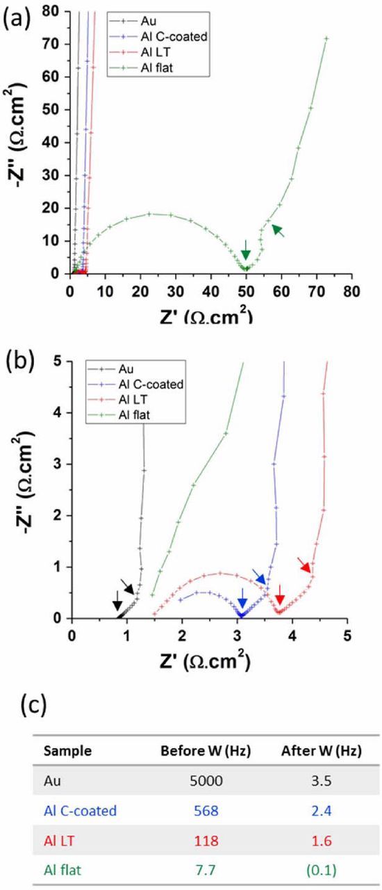
Figure 4. (a) Nyquist Plots of supercapacitor cells assembled with various current collectors. (b) Zoom on the 0-to-5 Ω.cm2 region. (c) Characteristic transition frequencies shown on the Nyquist plots (boundaries of the Warburg diffusion regime), corresponding to the arrows appearing in (a) and (b).
The main difference observed in the Nyquist plots is the size of the semi-circle appearing in the high frequency range. This semi-circle is associated with the charge transfer resistance of electrons tunneling through the alumina layer present at the aluminum surface. The resistance associated with this charge transfer was found to be 48 Ω.cm2 for the flat Al foil (in accordance with the literature7), 2.1 Ω.cm2 for the LT Al foil and 1.1 Ω.cm2 for the carbon-coated Al foil. It had a significant impact on the diffusion frequency range, shifting it toward lower frequencies (cf. Fig. 4c). As supercapacitor cells assembled with different current collectors used the same activated carbon active materials and electrolyte, the resistance associated with carbon particles and electrolyte ionic resistance should be almost the same, therefore the difference in charge transfer resistance is induced by different contact resistance between the active layer and the current collector. These results clearly demonstrate the impact of laser roughening of the Al current collector's surface, the interface charge transfer resistance being dramatically decreased (from 48 to 2.1 Ω.cm2). This is attributed to a combination of a much higher surface area and a better mechanical anchoring of the active layer onto the foil surface, these two phenomena providing a significant enhancement of the electronic flow between the layers. The C-coated Al current collectors were observed to enhance even more the electronic flow between the layers. This is possibly achieved through the elimination of the alumina layer before the application of the protective carbon coating. This treatment generally avoids the regrowth of the alumina by stabilizing the surface toward further oxidation.14,8 Besides, the carbon layer also enhances the anchoring of the carbon-based active layer.
The EIS data was further processed using theoretical calculations to extract the frequency behavior of complex capacitance from the cells.13 Figure 5 displays frequency dependence of the real (C') and imaginary (C") parts of the capacitance of the cells. The capacitance available from the cells is appearing as the low frequency plateau of the real capacitance C'. All cells reached comparable values except the one assembled with flat Al CCs. This is expected since the capacitance is related to the amount of activated carbon in the active materials. Because of its high internal resistance, the flat Al cell did not reach full capacitance in the frequency range investigated. The time constant of the cell (τ = RC; R being the cell resistance and C its capacitance) is defined as the value above which it reaches half of its capacity. This value can be used to estimate the power capability of a cell. It can be measured as the peak value of the imaginary part of the capacitance (C"). The time constants of the cells assembled with various CCs are shown in Fig. 5b.
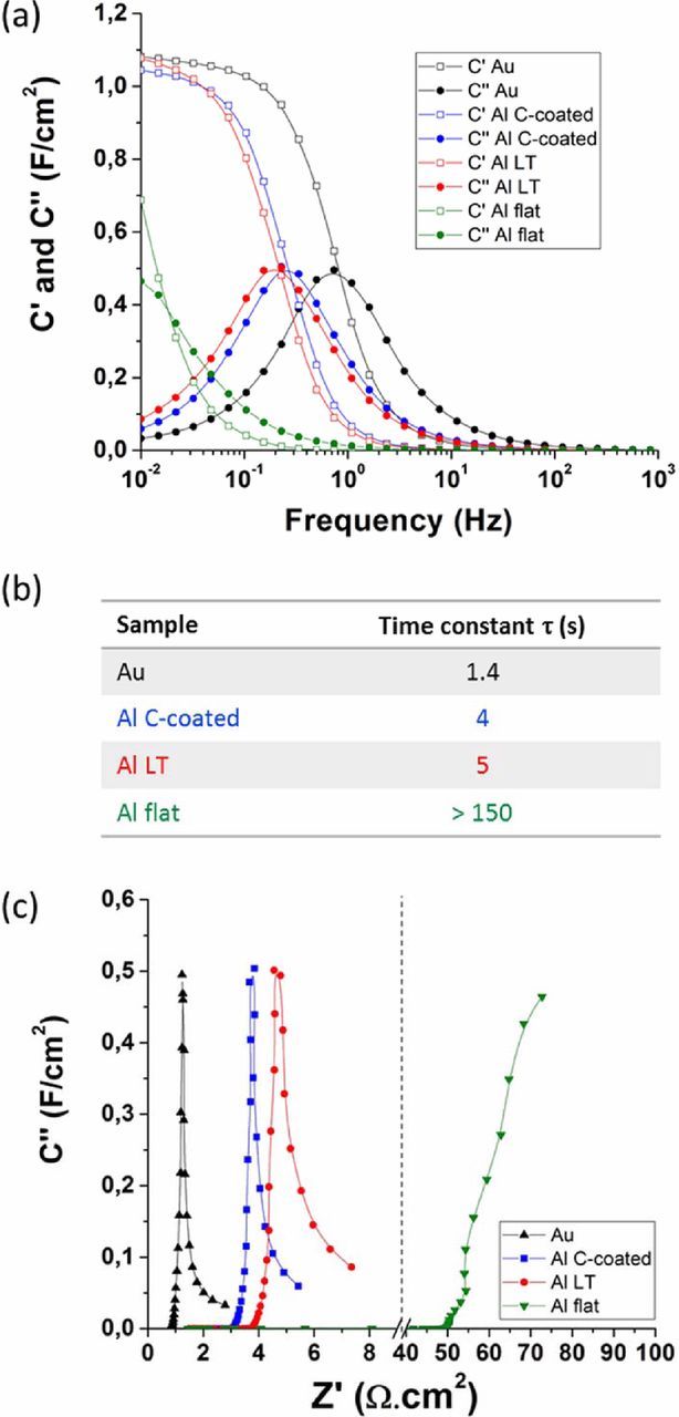
Figure 5. (a) Frequency dependence of the real (C') and imaginary (C") parts of cells assembled with various CCs (calculated from the EIS shown in Fig. 4); (b) Time constants of the cells as measured at the peak of the C" curves; (c) Imaginary capacitance vs. real resistance.
The cell assembled with gold CCs had a time constant of 1.4 s, approximately 3 times lower than that of cells having surface-engineered Al CCs. This clearly shows that one of the main limitations of the high power capability of supercapacitors is directly linked to the CC/active materials interface. Using flat untreated aluminum CCs appeared to significantly decrease the power output of the cell no matter the quality of the activated carbon, with a time constant > 150 s. The C-coated Al CCs gave a slightly lower time constant compared to the LT Al CCs, as already estimated from Fig. 4, based on the lower internal resistance and higher diffusion frequency range.
An even more visual representation of the impact of the CC/active layer's interface on the supercapacitor performance is obtained by plotting the imaginary part of the capacitance vs. the real part of the resistance, as recently developed by Banda et al.15 This plot allows to quickly differentiate the power capability of the cells as well as the type of resistances that explain the differences. In our study, the main differences observed between the cells, as shown in Fig. 5c, are a shift of the imaginary capacitance toward higher resistance. The shape of the curves themselves is not significantly impacted (except for the flat Al whose EIS characterization was incomplete between the chosen frequency ranges). These differences can be directly attributed to a high frequency electronic transfer (i.e. can be attributed to the CC/active layer interface), and differ radically from differences caused by ionic resistances (which cause a broadening of the curve, without any shift along the X-axis),16 or active materials electronic structure resistances (which impact both the peaks of capacitance and the shape of the curve).15
Even though EIS provides meaningful information on the power capabilities to be expected of the supercapacitors, it is important to test the performances of the devices by charging and discharging them under different regimes. Figure 6 displays charge-discharge cycles carried out using cyclic voltammetry (CV) at different scan rates. The cyclic voltammograms for the cell assembled with gold CCs displayed a typical carbon-carbon supercapacitor charging profile, with a quasi-rectangular shape. The shape was conserved even at high scan rates, with negligible polarizations effects until 500 mV/s. The cells assembled with LT Al and C-coated Al CCs both displayed quasi-perfect rectangular shapes at low scan rates, but showed increasing polarization when the scan rate was increased. On the other hand, the use of flat Al CCs caused strong polarization effects even at low scan rates. This confirmed the significant impact of the electronic charge transfer at the CC/active materials interface on the global performances of the supercapacitors.
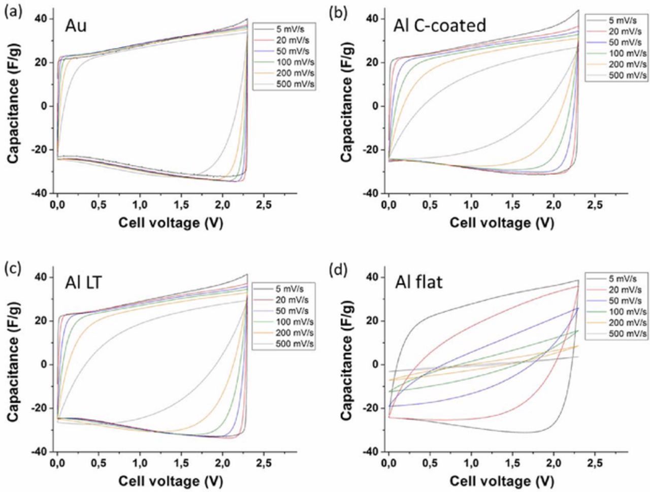
Figure 6. Cyclic voltammograms at various scan rates of supercapacitor cells assembled with the various CCs. (a) Au; (b) C-coated A; (c) LT Al; (d) flat Al.
Figure 7 presents the galvanostatic charge/discharge cycles (GC) of the supercapacitor cells at various currents. The curves show the characteristic linear progression of the voltage during charge/discharge of carbon-carbon supercapacitors. The cell capacity can be calculated from the slopes of these curves and the cell resistance can be determined from the voltage drop observed at the current switch between charge and discharge (the so-called "ohmic drop"). The ohmic drop being directly proportional to the current (following ohm's law dV = R.dI), the more current applied to the cell, the more important the ohmic drop will be. Figure 7 clearly shows that the supercapacitor cell assembled with gold CCs has the smallest internal resistance. Even at 400 mA (corresponding to 50 A/g), the ohmic drop is rather limited (0.34 V). Supercapacitors assembled with C-coated and LT Al CCs show similar trends, the C-coated one being able to sustain slightly better the high current regimes. On the other side Fig. 7d clearly shows that the cell assembled with flat Al CCs is unable to sustain currents above 25 mA (∼3 A/g). Figure 8 presents the cell capacities obtained from CV at different scan rates and GC at different current densities. The GC data was further analyzed to extract the specific power and energy from the cell, which were plotted in a Ragone plot, a clear representation the energy retention vs. power demand (cf. Fig. 8c). These graphs clearly show the performance variations caused directly by the use of different current collectors. Both CV and GC experiments pointed to the same results: gold CCs clearly demonstrated a very good capacity retention with increasing power demand. The surface-engineered Al CCs both showed a reasonable capacity fading with increasing power demand, and the flat Al CCs showed a quick capacity decline when increasing the power demand. These results align with the power capability trends expected from the results of the EIS experiments. Gold CCs were tested as an ideal reference in terms of interface with the active materials, because of its high electric conductivity and the absence of a passivation oxide layer at its surface. The performances depicted in Figs. 6 to 8 for supercapacitor cells assembled with gold CCs can therefore be attributed to the sole active layers + electrolyte system, which can serve as a reference for the active materials performance. The slight polarization observed at very high power demand can be attributed to the kinetic limitations caused by the diffusion of the ionic species in the micropores of the RP20 activated carbon.
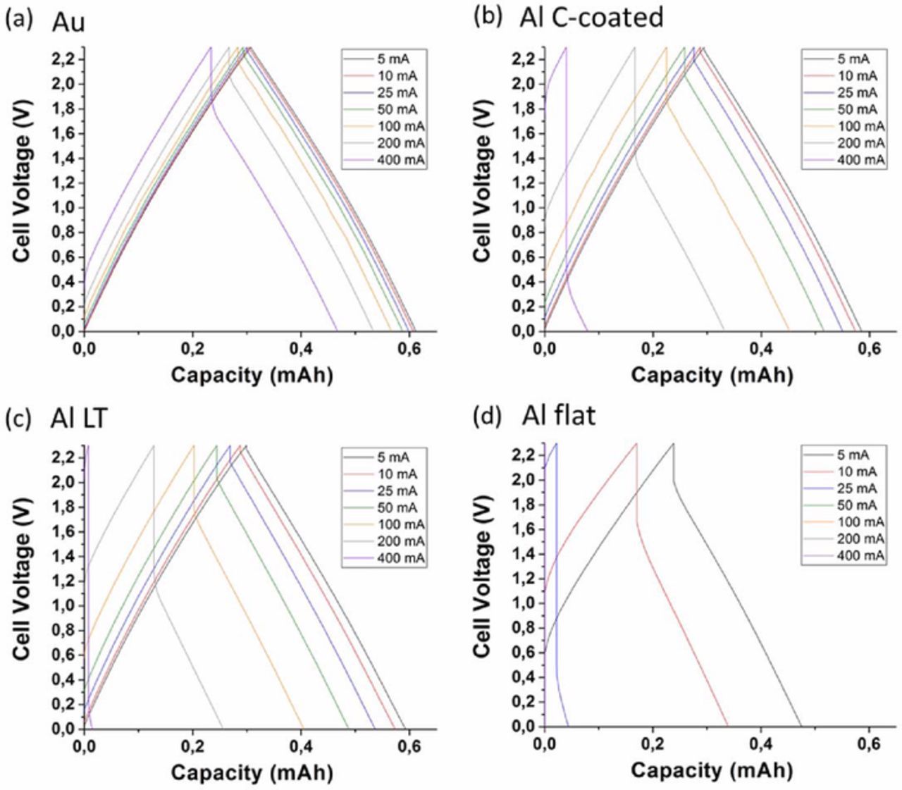
Figure 7. Galvanostatic charge/discharge cycling at various currents for supercapacitor cells assembled with (a) Au, (b) c-coated Al, (c) LT Al and (d) flat Al current collectors.
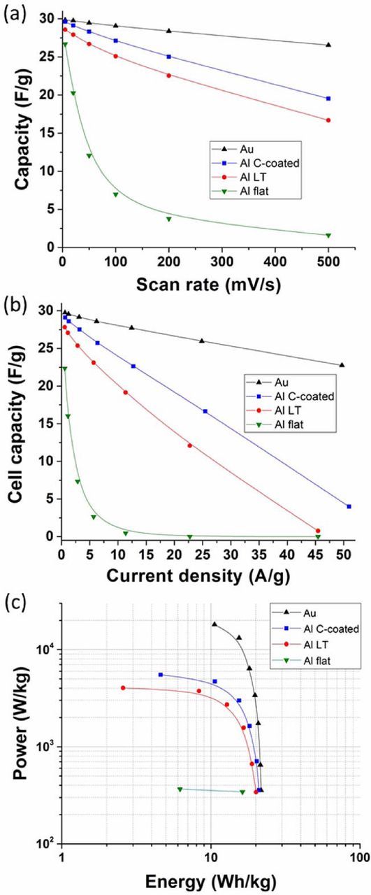
Figure 8. Power capability of the cells assembled with various current collectors: (a) cell capacity vs. CV scan rate; (b) cell capacity vs. GC current density; (c) Ragone plot (stack level) calculated from the GC experiments.
The second reference was a flat Al CC having its native aluminum oxide surface layer regenerated to erase the history of the material (cf. experimental section). The flat Al CC proved to be a very poor current collector, because of a high interface resistance with the active materials layer (cf. Figs 4–5). It is interesting to note that the flat aluminum CC not having a regenerated native alumina layer had a two-fold higher resistance (cf. Fig. S2). Alumina being an electronically insulating material, electrons have to tunnel through it. This process can become the kinetic limiting factor if the tunneling distance becomes too important. Typical thicknesses of a native alumina layer are in the order of 2–3 nm, and usually extend within a few days to 5 nm where the full passivation of the surface is reached.6 It is interesting to note that the two-fold difference in resistance of cells assembled with non-regenerated vs. regenerated alumina, relates quite well with the supposed thickness difference of the alumina layer. The electrochemical results presented in Figs. 6 to 8 clearly indicate that a flat Al surface does not provide a satisfactory interface with the activated carbon layer for fast electron transfer. This can be attributed to the presence of the insulating native alumina layer as well as a low surface area for electric charge transfer.
The laser treatment proved to be an efficient process to decrease the interface resistance by providing a significantly higher surface area (with surface features in the μm range, as show in Fig. 3 and Table II). This enhanced contact area allowed for an improved electronic transfer between the current collector and the active layers (cf. LT Al results in Figs. 6–8), which in turn dramatically improved the performances of the supercapacitor cells, from low to relatively high power demand (up to 3 kW/Kg according to Fig. 8c). According to the EIS experiments and data analysis, the improvement is effectively attributed to a better charge transfer, occurring both at lower resistance and higher frequencies. The semi-circle appearing in the Nyquist plot (cf. Fig. 4) still attests the presence of a native alumina layer at the surface of the LT Al foil, but its resistance to electron tunneling is significantly decreased (2.1 Ω.cm2, cf. Fig. 4a). Therefore, it is hypothesized that the improvement is mainly caused by a drastic increase in contact area. A better anchoring of the active layer on the roughened surface could also explain part of the improvement.
The commercially available carbon-coated current collector also showed a drastic improvement over the Al flat surface. This is also possibly obtained through an increase in surface area, brought by the carbon protective layer deposited on the aluminum foil (cf. Fig. S3). The anchoring and affinity of the carbon-based active layer with this protective carbon layer might also help enhance the electrical contact between the layers. Finally, the improvement might be achieved through the elimination of the alumina layer before the application of the carbon coating as explained above, though a semi-circle in Fig. 4 still proves the presence of a charge transfer that might be attributed to the presence of an alumina layer.
The supercapacitors performance stability was evaluated through continuous galvanostatic cycling at a current density of 12.5 A/g during 10,000 cycles. The results are presented in Figure 9. The cells assembled with different CCs display varying capacities even at the beginning even though their active layers only vary by 5 wt% at most. This is due to the different ohmic drop observed at the applied current density. According to Fig. 8b, the gold, C-coated Al and LT-Al CCs provide a capacity of respectively 27, 22 and 19 F/g when a 12.5 A/g current density is applied. The cell assembled with gold CCs showed only a 1.4% capacity fade over 10,000 cycles, demonstrating a perfect stability. The C-coated Al CCs showed a slight 2.8% decrease in capacity, also proving a nearly perfect stability.
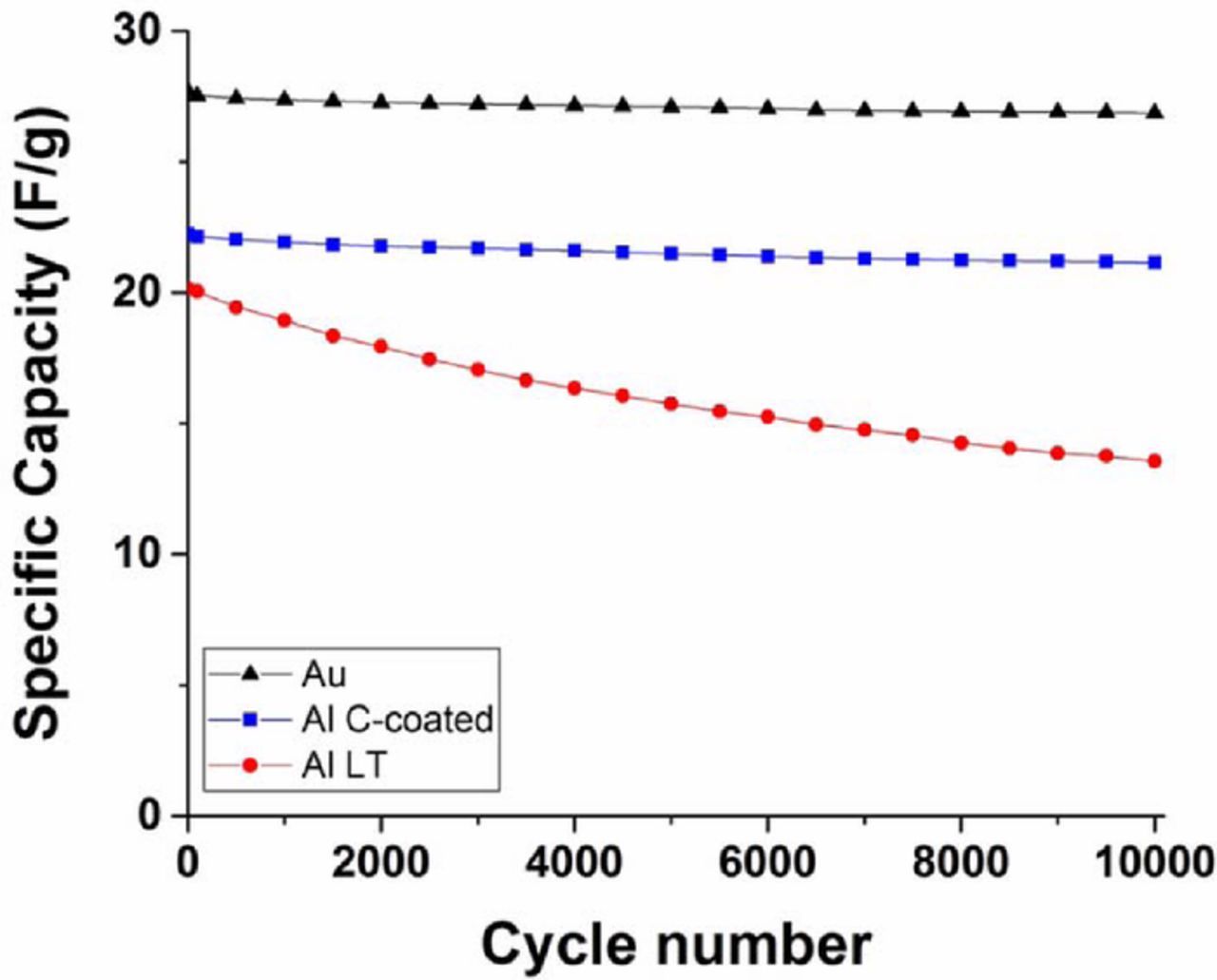
Figure 9. Performance stability of supercapacitor cells assembled with different current collectors, during galvanostatic cycling at a current density of 12.5 A/g (corresponding to 50 mA/cm2).
On the other side, there was a 17% capacity fading when using LT-Al CCs. Further investigation showed that the performance degradation was mostly related to the interface between the active layers and the CCs. While the slope of the GC curves remained essentially identical (as shown in Figure S4), the ohmic drop increased from 0.5 to 0.84 V during the cycling, indicating that the capacity fade was caused by an increase in cell resistance. EIS investigation showed that the semi-circle appearing in the Nyquist plot (attributed to electron tunneling through the alumina layer) increased from 2.1 to 4.35 Ω.cm2 (cf. Fig. S5a). It is also clearly observable in the imaginary capacitance vs. real impedance plot (cf. Fig. S5b), where the shape of the curve did not change much but was rather shifted toward higher resistance, demonstrating the increase in high frequency resistance vs. ionic resistance. It is interesting to note that the EIS data for the cell assembled with gold CCs was not impacted by the 10,000 cycles, whereas the C-coated AL also showed some increase in the resistance associated with the growth of the alumina layer.
A certain growth of the alumina layer is indeed expected for a non-protected aluminum CC, since it can reduce species (mostly impurities contained either in the electrolyte or in electrode formulations), especially when it is brought to high voltages, thereby oxidizing further its surface. Although the observed capacity fading shown in Fig. 9 for LT-Al can be certainly attributed to the re-oxidation of the surface of LT-Al, other causes, such as aggregation of conductive additive particles or appearance of micro-cracks between the active carbon layer and the Al foil may not be totally ruled out. These results indicate that the stability of LT-Al foils needs to be improved to enable their use as CCs for high performance supercapacitors, for example by applying a protective coating after laser treatment.
Conclusions
The laser ablation technique has been used in this study to roughen Al foils in a high vacuum chamber. By varying laser ablation process parameters, various microstructural surface features and roughness of Al foils with oxide free surface were successfully produced. The supercapacitor cells assembled with laser surface roughened Al foils exhibited lower interfacial resistance and higher specific capacitance than supercapacitor cells assembled with flat Al foils. The results revealed that the laser surface treatment significantly enhances the electronic contact area between the current collector and the active material layers. However, the stability of laser surface roughened Al foils during cycling is still not as good as carbon-coated Al foils due to the growth of Al2O3 layer during cycling. A combination of laser surface roughening and protective coatings is suggested to optimize Al current collectors for high power supercapacitors applications. This work demonstrates that laser ablation in vacuum conditions is a promising technique for the preparation of oxide free Al current collectors for supercapacitors due to its excellent flexibility and capability of controlling microstructures, surface roughness and areas.
In our next communication, research work on seeking the best coating materials and processes for protecting laser surface roughened Al foils will be reported.
Acknowledgments
The authors would like to thank NRC's Vehicle Propulsion Technologies program and Natural Resources Canada (PERD program) for funding this project. The authors are also indebted to their NRC colleagues: Dr. Lei Zhang and Dr. Christina Bock for their collaboration in the supercapacitor research project. The authors also want to acknowledge Brian. Gibson, Craig Dinkel and Marco Zeman of NRC-London for their technical assistance.
ORCID
Dongfang Yang 0000-0003-3804-9726
Alexis Laforgue 0000-0003-3848-7531