Radiation Defects Nano-Scale Inhomogeneous Distribution Influence on Apparent Hall Mobility in Silicon
Temur Pagava, Levan Chkhartishvili
DOI10.21767/2471-9838.100027
Temur Pagava and Levan Chkhartishvili*
Department of Engineering Physics, Georgian Technical University, Merab Kostava Avenue 77, Tbilisi, 0175, Georgia
- *Corresponding Author:
- Levan Chkhartishvili
Department of Engineering Physics, Georgian Technical University, Merab Kostava Avenue 77, Tbilisi, 0175, Georgia.
Tel: + 995 599 340 736
E-mail: chkharti2003@yahoo.com
Received Date: August 21, 2017; Accepted Date: September 11, 2017; Published Date: September 14, 2017
Citation: Pagava T, Chkhartishvili L. Radiation Defects Nano-Scale Inhomogeneous Distribution Influence on Apparent Hall Mobility in Silicon. Nano Res Appl. Vol. 3 No. 3:10. DOI: 10.21767/2471-9838.100027
Abstract
Temperature dependencies of charge carrier Hall concentration and Hall mobility are systematically studied within the range 77 to 300 K for both n- and p-type silicon crystalline samples irradiated with high energy protons or electrons and annealed at temperatures up to 380°C and 600°C, respectively. In some cases, measured at a fixed temperature hall mobilities are found to be significantly lower or significantly higher than those in non-irradiated material. These results are interpreted on the basis of assumption that secondary radiation defects in silicon form clusters with conductivity significantly different from that of the surrounding matrix. A phenomenological theory, recently introduced by authors, explains apparent Hall mobility minima revealed on the temperature-dependence curves. Clusters themselves should possess high conductivity (be “metallic”), but in certain conditions they effectively act as (“dielectric”) clusters with low conductivity, because they can be screened by the shells consisting of defects capturing charge carriers.
Keywords
Radiation defects; Apparent hall mobility; Silicon
Introduction
Our previous studies [1-4] devoted to the secondary defects formation in silicon irradiated with high-energy particles lead us to the conclusion that measured at a fixed temperature charge carriers Hall mobility, significantly lower or significantly higher than those in non-irradiated material, is related to the inhomogeneous distribution of radiation defects in the samples [5-7].
Here we quote only our recent works and not all the numerous papers, in which information on the temperature dependences of the electro-physical parameters of silicon irradiated by highenergy particles is reported. The fact is that we have restricted ourselves by the cases when the measured carriers Hall mobility significantly differs from the Hall mobility in the material before irradiation at the same temperature. In brief, the history of the introducing of this problem is as follows.
A strong decrease in the Hall mobility of current carriers in an irradiated semiconductor was reported in study by Golubev et al. [8]. The authors unsuccessfully tried to explain this experimental result by changing the charge-state of the carriers scattering centers. As far as we know, for the first time Milevsky et al. related [9] a substantial decrease in the Hall mobility of the current carriers in irradiated silicon with the creation of inclusions in the form of clusters of defects. Later, a structural model of such inclusions was developed by Kuznetsov and Lugakov [10] and an expression was obtained for the mobility of current carriers, when they are scattered by inclusions [11]. In recent years, we have found that the inhomogeneity of the material can not only significantly decrease but also increase the Hall mobility.
Present work aims to reveal physical mechanism of strong influence of inhomogeneous distribution of radiation defects on charge carriers Hall mobility in irradiated silicon. Of course, the explanations based only on Hall measurements data remain mostly tentative and speculative and the follow-up, in particular, structural studies are desirable.
Solution of the stated problem possesses not only academic, but also practical importance. On the basis of such solution, it can be developed the producing technologies for semiconducting materials with charge carrier’s effective mobility variable in wide range.
From the papers aim, it seems obvious to use the Hallmeasurements as main tool of the investigation.
Temperature dependencies of charge carries Hall concentration and Hall mobility are systematically measured up to room temperature for both n- and p-type silicon crystalline samples irradiated with high energy protons or electrons, respectively, and then annealed at temperatures up to 380°C and 600°C.
Experimentally obtained results are interpreted based on assumption that secondary radiation defects in silicon (their identifications with corresponding electron energy levels are taken [12] form clusters with conductivity significantly different from that of the surrounding matrix.
Recently suggested phenomenological theory is utilized to explain apparent Hall mobility minima revealed on the temperaturedependence curves. There is made conclusion that clusters themselves should possess high conductivity, but in certain conditions they act as clusters with low conductivity because they can be screened by the shells containing defects effectively capturing the carriers.
Materials and Methods
In the range of temperature T from the nitrogen boiling point up to room temperature, using the Hall method the temperaturedependences of majority charge carrier’s concentration and mobility are measured in FZ- (obtained by floating-zone melting method) and Cz- (obtained by Czochralski method) silicon crystals irradiated with high-energy particles at room temperature and subsequently isochronously annealed at various fixed temperatures during 10 min. The strength of magnetic field used in Hall measurements was 1500 G.
Such kind measurements are principally not fully-repeatable because initial samples and conditions of their irradiation and annealing cannot be fully-repeatable. Therefore, it is impossible to provide the technical repeats numbers of these curves. However, we can estimate the Hall-measurements accuracy itself.
In the temperature range of measurements, the dominating scattering mechanism related to scattering by acoustic phonons remains the same. Corresponding Hall-factor equals to 1.18 and, therefore, uncertainty factor for carrier’s concentration is 1/1.18≈0.85. Thus, the expected errors are within ~15% because this value significantly exceeds the standard relative errors in measuring temperature and resistance.
There are chosen such irradiation doses, for which material remains semiconducting. Upon irradiation, the samples were blown with compressed air to prevent their overheating. The heterogeneity of the particles flow was less than 7%.
n-type silicon
The FZ n-Si crystals containing oxygen O in concentration of ~1016 cm-3 were doped with phosphorus P. The electrons concentration n and mobility μn at room temperature were equal to ~5.5 × 1013 cm-3 and ~1400 cm2/V· s, respectively. They were irradiated with 25 MeV protons (with pulse duration of 25 μs and repetition frequency of 0.25 Hz) at dose of 8.1 × 1012 cm-2. Samples were annealed at temperatures up to 380°C.
Obtained dependences n=n (T) and μn=μn (T) are shown in Figures 1 and 2.

Figure 1: Electrons Hall concentration versus temperature in n-Si crystals 1–before irradiation ( ), 2–after irradiation (
 ) and annealing at temperatures 3–110 (
 ), 4–120 (x), 5–290 (
 ), and 6–380°C (
 ).
).

Figure 2: Electrons Hall mobility versus temperature in n-Si crystals 1-before irradiation (•), 2- after irradiation () and anneal-ing at temperatures 3 - 110 (), 4- 120 (x), 5- 290 (), and 6- 380°C ().
p-type silicon
The Cz p-Si crystals containing oxygen O in concentration of ~1018 cm–3 were doped with boron B. The holes concentration p and mobility μp at room temperature were equal to ~6.0 × 1013 cm–3 and ~500 cm2/V·s, respectively. They were irradiated 8 MeV electrons (with pulse duration of 3.5 μs and repetition frequency of 0.25 Hz) at dose of 5.0 × 1015 cm–2. Samples were annealed at temperatures up to 600°C.
Obtained dependences p=p (T) and μp =μp (T) are shown in Figures 3 and 4.

Figure 3: Holes Hall concentration versus temperature in p-Si crystals 1- before irradiation (), 2- after irradiation () and annealing at temperatures - 80 (), 4 -90(x), - 120(), 6- 170 (), 7- 180 (+), 8- 380 ( ), 9- 470 (
 ), and 10- 600°C (
 ).
).

Figure 4: Holes Hall mobility versus temperature in p-Si crystals 1- before irradiation (), 2- after irradiation () and annealing at temperatures 3- 80 (), 4 -90(x), 5- 120(), 6- 170 (), 7- 180 (+), 8- 380 (), 9- 470 (), and 10- 600°C ().
Results
n-type silicon
In the following analysis of the obtained results, we take into account that in irradiated zone-melted n-Si crystals the main radiation defects are: A-center-complex of a vacancy with a residual oxygen impurity OV, doubly and singly negatively charged divacancies V2-- and V2-, and E-center-complex of a vacancy with phosphorus dopant atom PV, energy levels of which are placed from the conduction band edge at distances of 0.17 eV, 0.23 eV, 0.39 eV and 0.44 eV, respectively. The concentration of A-centers, divacancies V2, and E-centers in tested n-Si samples are estimated as: 3.2 × 10¹³, 1.2 × 10¹³, and 1.0 × 1013 cm–3. The sum concentration of thermally stable (with annealing temperature above 500°C) multi-vacancional complexes is 2.1 × 1013 cm–3. All these concentrations of radiation defects are determined from the analysis of the dependences of electrons concentrations at fixed temperatures on the samples annealing temperature.
The Curve 1 in the Figure 1 corresponds to the initial sample (before its irradiation and annealing). It indicates almost complete ionization of dopant centers and, therefore, the constancy of the conduction electrons concentration in the entire temperature range of measurements.
The counterpart Curve 1 in the Figure 2 presents the temperaturedependence of electrons mobility, which is typical for nonirradiated silicon displaying scattering the electrons by phonons.
The Curve 2 in the Figure 1 corresponding to the irradiated, but not yet annealed, sample shows a strong decrease in the measured values of electrons Hall concentration. This behavior is due to the fact that most part of dopant phosphorous atoms forms complexes with the radiation (and, therefore, nonequilibrium) vacancies, i.e., E-centers.
According to the Curve 2 in Figure 2, it is clear that irradiation leads to a significant increase in the measured values of the electrons Hall mobility. This kind of behavior finds its unambiguous explanation only in the fact that the irradiation makes crystal heterogeneous by conductivity. Namely, the relatively highly conductive, so-called “metallic” inclusions should be formed. According to the galvanomagnetic theory of heterogeneous materials [13], If semiconductor sample contains “dielectric” (“metallic”) inclusions with conductivity significantly lower (higher) than that of matrix, the apparent (measured) value of the charge carriers Hall mobility would be lower (higher) than that in matrix. Consequently, significant increase in Hall mobility after irradiation points to the formation of “metallic”, i.e., with higher than in the rest matrix conductivity, inclusions.
The fact is that, along the proton tracks the irradiation creates the primary radiation defects capable to be associated and form various vacancy complexes and clusters, which further can transform into “dielectric” or “metallic” inclusions. As the stresses related to these inclusions attract point defects from the matrix, their concentration increases around the inclusions there are formed their impurities-structural defects “shells”. It yields the increase in energy of electrostatic interaction between charged point centers. In n-Si the increased electrostatic interaction between negatively charged defects leads to a decrease in the average ionization energy via electron transitions in the conduction band. The amount of such reduction depends on the ionization energy initial value and the filling of the defects presented in the crystal. Thus, there are two competing processes. On the one hand, at fixed ionization energy, the increasing in the temperature leads to the increasing in free electrons concentration. But, on the other hand, the deionization of negatively charged centers reduces energy of their electrostatic interaction and then increases mean ionization energy.
Annealing at 110°C (Curve 3, Figure 1) increases the electron concentration and leads to the n(T) curve with two minima at ~155 and ~205 K. The detected oscillatory temperaturedependence of the electrons concentration can be explained by the presence of an electrostatic interaction between the negatively charged point defects when they are presented at sufficiently high concentrations around “metallic” inclusions.
Note that, because after an annealing cycle Hall measurement are not repeatable and also for small number of data points positions of these (and other) mobility minima can be determined only in a crude approximation.Reducing the Hall mobility after annealing at 110°C (Curve 3, Figure 2) can be explained by the appearance of impuritiesstructural defects “shells” around the “metallic” inclusions. During such low-temperature treatment, there are annealed the secondary radiation defects with low thermal stability, including E-centers. The products of their decomposition tend to “metallic” inclusions and create above noted shells. A shell itself is “metallic” (like the inclusion itself) or “dielectric” and, consequently, shielding “metallic” inclusions from conduction electrons depending on the temperature and degree of filling of defects by electrons.
At 110°C, in the result of the annealing of vacancy-containing defects with low thermal stability the non-equilibrium vacancies are formed. They tend to the disordered regions in the form of “metallic” inclusions and increase the defects concentration around them. There intensive transfer of electrons in the conduction band begins from negatively charged A-centers at lower temperatures than in a homogeneous material (with energy level at 0.17 eV). Therefore, at relatively low temperatures the electrons concentration exceeds its equilibrium value at the same temperature in the homogeneous sample. With increasing in temperature, the concentration of charged A-centers and, consequently, energy of electrostatic interaction between neighboring defects decrease that leads to the opposite effectdecreasing in the electrons concentration.
With further increase in the temperature, similar processes occur with the doubly negatively charged divacancies with the energy level at 0.23 eV. Each divacancy transfers one of the two trapped electrons in the conduction band and the conduction electrons concentration increases again. All this means the appearance of the first minimum on n(T) curve in the vicinity of ~170 K. As for the second minimum, which is located in the vicinity of ~240 K, seemingly the deionization of singly negatively charged divacancies with the level at 0.39 eV is responsible for its appearance. Of course, because of high-energy proton irradiation, in the silicon matrix there are formed other vacancy complexes as well. But, charge states of these centers do not change in the vicinity of mentioned minima.
For the sample under the consideration locations of mobility peaks on the temperature axis, ~190 and ~240 K correlate with the concentration minima, ~170 and ~240 K. Therefore, their appearance can also be related to recharging of levels at 0.23 eV and 0.39 eV, respectively.
The Curve 4 (Figure 1) corresponds to the annealing of many of E-centers at 120°C. This process significantly reduces the electrostatic interaction and therefore oscillatory temperaturedependence of electrons concentration is no longer observed. Moreover, thanks to returning many of phosphorus dopant atoms in the matrix the total concentration of the conduction electrons is increased additionally. It should be noted in regard to E-centers that because the depth of the corresponding energy level, 0.44 eV, within our measurements temperature range the vast majority of them does not change their chargestate- they always remain single-negatively charged. Therefore, these centers do not directly affect the concentration variation with temperature. Although they do this indirectly, through the electrostatic interaction.
After annealing of E-centers at 120°C (Curve 4, Figure 2), the μn(T) curve shifts up because now the reduction in the effective mobility is related only to the doubly charged divacancies and values of mobility are additionally reduced in the range 115 to 130 K, where A-centers are no longer charged.
At 290°C (Curve 5, Figure 1), there are annealed the divacancies. This causes further upward displacement of the curve.
After annealing of divacancies at 290°C the μn(T) dependence shifts down (Curve 5, Figure 2), closer to the initial one. Now mobility reduces in the range 85 to 100 K, where A-centers are charged.
At 380°C (Curve 6, Figure 1) annealing of A-centers ends the annealing of all the significant point radiation defects in the crystal and thereby almost the initial constancy of the electrons concentration is restored. Although the value of the electrons concentration remains something lower because of the presence of disordered regions induced by irradiation. They finally can be annealed only at higher temperatures (above 600°C).
When A-centers are annealed at 380°C (Curve 6, Figure 2), all the additional (radiation defects related) mechanisms of electron scattering disappear and almost initial electrons mobility (determined by phonon scattering) is restored as well.
p-type silicon
In the following analysis of the obtained results, we take into account that in irradiated Cz p-Si crystals the main radiation defects are: so-called H1-centre- a divacancy-related donor, divacancy V2, and so-called H2-centre- complex of dopant boron atom with divacancy BV2, energy levels of which are placed from the valence band edge at distances of 0.22 eV, 0.28 eV, and 0.45 eV, respectively. The concentration of H1-centers, divacancies V2, and BV2-centers in tested samples can be estimated as: 3.5 × 10¹², 8.0 × 10¹², and 4.5 × 1012 cm–3. As for other centers detected, their concentrations are: K-centers (complexes containing C, O and vacancies: CO, COV or, more probably, COV2)- 3 × 10¹³, oxygen / vacancy complexes O2V3 and O3V3 together- 2 × 10¹³, oxygen/vacancy complexes OV2 and OV3 together- 1 × 10¹³, interstitial carbon Ci and multivacancional complex V4 together- 6 × 10¹², and boron-vacancy complex BV- 5 × 1012 cm–3. All these concentrations of radiation defects are determined from the analysis of the dependences of holes concentrations at fixed temperatures on the samples annealing temperature.
Based on the temperature-dependences of holes concentration before and after irradiation and after annealing at different temperatures shown in Figure 3, the concentration changes for the holes and some of radiation-induced defects can be described in the following way.
In the annealing temperature interval 170°C to 200°C, the sharp increase in holes concentration can be associated with the annealing of defects with the energy level of BV complex, 0.45 eV, and the concentration of 5 × 1012 cm-3. These centers are quite deep acceptors and, therefore, up to room temperature their majority is positively charged by the capturing of holes.
In the interval 270° to 300°C, a defect with the energy of 0.28 eV and the concentration of about 8 × 1012 cm-3 is annealed. For 10 min isochronous annealing conditions, these values correspond to divacancy V2.
In the course of divacancies annealing, a drastic increase of the concentration of defects with the donor level at 0.22 eV. So, called H-centers- is observed. Moreover, the concentrations of the divacancies decayed in the interval 270° to 290°C and the emerged H-centers are equal to each other. It testifies that, H-centers do contain divacancies. In the Figure 3, the third step from below in the step-like Curve 6 corresponds to the transition of electrons from the valence band onto a donor level 0.22 eV, which increases the holes concentration. Process comes to the end after annealing at ~490°C.
In the course of formation, the divacancies-related donors located at 0.22 eV take away their electrons from the valence band. Therefore, the value of holes concentration shows grow at divacancies annealing, although we have practically constant holes concentration in the interval of annealing temperatures 270°C to 290°C. Probably, the complexes, which are formed at divacancies, contain boron atoms. The concentration of boron atoms, which become locked at the formation of H-centers and of the majority charge carriers, which are formed at divacancies annealing, are almost equal. Therefore, the variation of the concentration is zero in this annealing interval.
These results are in agreement with the opinion about the existence of BV2 complexes of substituting, i.e., dopant, boron atoms in irradiated p-Si crystals, which are finally annealed in the temperature range of 330°C to 400°C.
Let us note that the activation energy of the divacancies migration is 1.30 eV, i.e., less than their binding energy 1.47 eV. Therefore, divacancies can migrate without decaying over the crystal. On the other hand, BV complexes are annealed at a temperature of about 180°C and, consequently, cannot participate in the formation of BV2 complexes at temperatures of 270°C to 290°C. So, it is possible to assume that, BV2 complexes are formed by means of direct conversion of divacancies: B+V2→BV2, rather than the consequence trapping of a pair radiation-induced vacancies V by B atom in the silicon lattice site.
Centers of H-type are annealed in two stages, in the ranges of 300-320 and 360°C to 440°C. The initial concentration of H1- centers is equal to 3.5 × 1012 cm-3, and the same number of centers is annealed at the first stage. At the second stage, the concentration of decayed centers coincides with that of BV2 complexes formed at divacancies annealing. Thus, we can assume that BV2 complexes are formed at 270°C to 290°C in the course of divacancies annealing and dissociate at temperature of 400°C. Concerning the H2-centres annealed at the second stage, 360°C to 440°C, they are identical to BV2 complexes by the ionization energy.
The variation of holes concentration after the annealing at 300°C can be associated with the decay or formation of O2V2- complexes, so-called K-centers, formed as a result of trapping of divacancies by CO-centers, and other deep centers (like above mentioned oxygen/vacancy complexes OV2, OV3, O2V3, and O3V3 and boron/divacancy complex BV2 ) characterized by the high thermal stability.
The Figure 4 shows the curves of the temperature-dependence of holes mobility from the nitrogen point up to room temperature. As seen, immediately after the irradiation holes mobility drops sharply and continues to decrease with increasing in annealing temperature (Curves 1 and 2, Figure 4).
After annealing at 90°C (Curve 4, Figure 4), a deep minimum appears in the temperature-dependence. After annealing at 120°C (Curve 5, Figure 4), the curve with a minimum move upwards, and after annealing at 180°C, it finally disappears, while the temperature-dependence itself is sharply enhanced (Curve 7, Figure 4).
High values of mobility obtained in irradiated samples by Hall measurements after their annealing at high temperatures point to the formation of the “metallic” inclusions. The significant decrease in the mobility immediately after the irradiation, presumably is due to the electrostatic screening of highly conductive atomic clusters by the secondary radiation defects of donor-type: the capture of holes makes them positively charged. Such inclusions affect the mobility in two ways-as “dielectric” inclusions they block the holes current and thus reduce the actual volume of the crystal, and as static electric charges at low temperatures they effectively scatter holes. All these lead to a decrease in the holes mobility both in the phonon- and chargedcenters- scattering temperature-ranges.
Further reduction in the mobility at initial stages of isochronal annealing (80°C to 90°C) must be caused by the negative annealing of the donor-type secondary radiation defects responsible for holes screening. This negative annealing process seems to be caused by the formation of new donor-type defect centers from the vacancies, which are products of dissociation of the disordered regions.
Non-monotonic temperature-dependence (presence of a minimum in the curve) of the holes effective Hall mobility is explained by the non-monotonic variation of the degree of screening with samples temperature (Curves in Figure 4).
As the temperature decreases from 300 K to 200 K, the degree of filling of radiation defects, which screen the inclusions, increases. Accordingly, it increases the degree of screening of atomic clusters, what leads to a decrease in the effective Hall mobility.
In the vicinity of 200 K, the energy of electrostatic interaction between the positively charged centers in impurities-structural defects shells around the atomic clusters reaches a critical value comparable with the ionization energy of the corresponding deep levels and it starts their deionization.
The effective mobility starts to grow, and a minimum appears on the temperature-dependency curve. Judging from the temperature range (90°C to 200°C) of the annealing of defects screening the shells around the “metallic” inclusions, they are complexes BV.
The observed oscillations of the holes Hall mobility in irradiated p-Si samples subjected to isochronous annealing at the constant rate of increasing in temperature, presumably are due to the changes in the degree of screening because the formation or annealing of different radiation-defects affecting the screening.
Highly conductive p-type clusters themselves are fully annealed at 600°C (Curve 10, Figure 4).
Results and Theorizing
Recently, we have proposed a phenomenological model [14] describing the temperature-dependence of charge carriers measured Hall mobility in a semiconductor inhomogeneous by conductivity. Model is based on following assumptions:
-Charge carriers obey the Boltzmann statistics;
-Temperature-dependence of their mobility in homogeneous (without inclusions) sample is as
 (1)
(1)
where m>0 is the dimensionless exponent; and
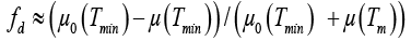
-The dominating energy level E trapping the charge carriers referred to the corresponding band edge is sufficiently deep to meet the condition
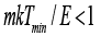 (2)
(2)
where Tmin is a minimum point for mobility.
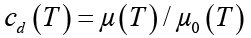
One of the main parameters of this model is the coefficient cd(T) determining ratio of Hall mobilities μ(T) and μ0(T) at given temperature T for the sample with “dielectric” inclusions and homogeneous sample–without inclusions with conductivity different from the rest part of the sample:
 (3)
(3)
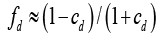
It is clear that,
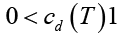 (4)
(4)
In general, the value of cd coefficient is determined by the volume fraction fd, as well as size, shape, and orientation of “dielectric” inclusions relative to the electric current direction, inter-connections between inclusions, crystal temperature, etc. But frequently only the volume fraction plays critical role and for “dielectric” inclusions of nearly spherical shape we have
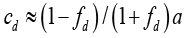 (5)
(5)
or
 (6)
(6)
Otherwise, the model analysis determines same parameter at a minimum point Tmin by the formula:
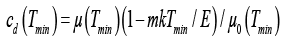 (7)
(7)
Let us note that the molar thermal energy of the crystal at room temperature is k T ≈ 0.025 eV. As for the trapping levels in silicon responsible for the screening of “metallic” inclusions and making them “dielectric”, they are quite deep- ranged from 0.17 upto 0.45 eV. The scattering of charge carriers by the acoustic phonons in homogenous silicon leads to the exponent value of m=3/2. Thus, within the temperature-range of measurements, the condition (2) for silicon is satisfied within a larger margin:
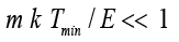 (8)
(8)
This fact allows the easy estimation of cd parameter in the vicinity of a minimum point from the relation (7):
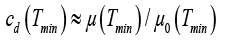 (9)
(9)
Finally, relations (6) and (9) approximately determine the volume fraction of the “dielectric” inclusions
 (10)
(10)
The Table 1 summarizes estimates of volume fractions of inclusions in measured by us samples. One can see that in all cases volume fractions of disordered regions consisting of “metallic” core and “dielectric” shell is too high, tens of percent.
The concentration in tested samples not exceeds 1014 cm-3. Then, maximal concentration of ionized scattering centers is 1014 cm-3. In such conditions, carriers scattering in silicon is mainly determined by phonons. For this reason, in above calculations we can neglect the differences by drift mobilities between matrixes of differentially irradiated and annealed samples. Of course, in “metallic” inclusions, the reducing of drift mobility maybe more palpable.
Thus, the total volume fractions of “metallic” and/or “dielectric” inclusions in silicon irradiated with high-energy particles can be estimated from the temperature-dependence of charge carrier’s mobility. However, the data obtained by Hall measurements are insufficient for estimation the formation probabilities of these large-scale defects. Only could be said that their concentration should be significantly lower than dopants concentration in the material, i.e., <1013 cm–3 in the case under the consideration.
As for the concentration of primary radiation defects, their concentration can be estimated as ratio of irradiation dose and depth of particle penetration.
We have determined depths of penetration of 25 MeV protons in n-Si samples of special form by measuring resistivity at two different doses 1.0 × 10¹² and 3.0 × 1012 cm–2 as 0.26 cm and 0.29 cm, respectively. The linear extrapolation to the applied dose of 8.1 × 1012 cm–2 yields the value of 0.37 cm, which well coincides with value yielded from the linear extrapolation of the energydependence recommended in the literature for the depth of proton penetration in silicon [15].
So, there are expected 8.1ÃÆâÃâÃâ Ãâââ¢1012/0.37≈ 2.2 ÃÆâÃâÃâ Ãâââ¢1013 primary defects per cm3 in the proton-irradiated silicon. Because of its heaviness high-energy protons can create primary defects in form of disordered regions. At least hundreds of neighboring regions have to agglomerate to form a single inclusion in the n-Si matrix.
The above estimated value of the penetration depth of 25 MeV protons is supported by the experimental data, e.g., by the ones presented in the study by Tschalär and Maccabee [16]. Its correctness also can be based on the assumptions which entail obtaining the number of displaced atoms equal to ~ 400 cm–2.s for such protons [17]. A similar production rate of displacement for ~25 MeV protons was obtained earlier in 1948 [18]. The production rates of Frenkel pairs were recently estimated using Hall measurements for 8 MeV and 15 MeV proton irradiation of silicon by Emtsev et al. [19]. On the one hand, all these data are an evidence of a dominance of elastic scattering of 25 to 50 MeV protons. But, on another hand, it does not mean that the probability of appearance of the recoil atom with the energy which would have been enough for creating a disordered region or a cluster of structural point defects in the silicon crystal subjected to irradiation with 25 MeV protons is small.
The point is that, according to the review on displacement damage effects in silicon [20], for ~ 20 MeV protons the recoil energy is estimated to be only of 12 to 20 keV. As the proton energy significantly exceeds the recoil energy, any isolated act of high-energy proton scattering by the silicon lattice seems to be almost elastic. However, in their turn such recoil energies significantly exceed atoms displacement energy–energy of vacancy–interstitial (Frenkel) pair formation in silicon, which equals only to ~13 eV [21]. It is reason why at high proton energies, it takes place the many sub-cascade scattering accompanied by the formation of high number Frenkel pairs.
What kind of radiation defects clusters/disordered regions we have to bear in mind? Because in silicon vacancies are much more mobile and reactive with impurities and other structural defects than interstitials, these clusters/disordered regions are expected to be enriches with interstitial atoms and impurities and also some vacancy-containing complexes. In this regard, it is expedient to note that interstitials are characteristic for irradiated IV Group semiconductors in general [22].
Approximately, the depth d of electron penetration in solids can be calculated by the following formula:
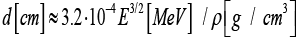 (11)
(11)
where E is the mean energy of electrons in the beam and ρ is the density of the material [23]. For silicon, ρ≈2.33 g/cm3, irradiated with E=8 MeV electrons we get d≈0.0031 cm. So, at the dose of 5.0 × 1015 cm–2 there are expected 5.0 × 10¹⁵ / 0.0031≈1.6 × 10¹⁸ primary defects per cm3 in the p-Si sample. Because of lightness of electrons, almost all of them are point structural defects. Thus, at least millions of defects are comprised by the inclusions formed in irradiated p-Si.
Discussion
Thus, a certain dose of irradiation of high-energy particles and certain subsequent thermal treatment of silicon crystals leads to a significant increase in the majority charge carriers Hall mobility measured in fixed temperature ranges. The possibility of such behavior clearly points to the heterogeneity of the irradiated samples by local conductivity. Namely, in these cases the exposure of the silicon crystals leads to the formation of relatively high-conductive-“metallic”-inclusions in them.
Note that in the two samples presented by us, the manifestation of this effect is not quite the same: in the n-Si crystal irradiated by 25 MeV protons electrons Hall mobility significantly increases immediately, while the p-Si crystal irradiated by 8 MeV electrons an essential increase in the holes Hall mobility shows only after annealing.
To explain this discrepancy, first note that the “metallicity” of inclusions in the semiconductor matrix means the locally increased concentration of dopants. Therefore, it is natural to assume that any such inclusion is surrounded by an increased concentration of secondary radiation defects in the form of complexes of primary radiation defects (vacancies and interstitials) with dopant atoms. In this approach, the masking of the “metallic” inclusions in irradiated p-Si should be associated with vacancy-containing complexes of B dopant atoms.
But it seems that this is not the only possible cause. For comparison, we note that the n-Si crystal also contains high concentration of P dopant atoms, but concentration of complexes of phosphorus with radiation defects is not sufficient for screening “metallic” inclusions occurring immediately after exposure.
Conclusion
Most likely, a different behavior is mainly due to the difference in the energies of bombarding particles. The particles of energy of 25 MeV produce larger inclusion than that of energy of 8 MeV. Hence in the first case for the screening a higher concentration of radiation centers around the inclusions is needed. For their sources can serve only the annealing processes producing a large number of non-equilibrium vacancies.
References
- Pagava TA, Kutelia ER, Maisuradze NI, Eristavi BG, Chkhartishvili LS (2005) Influence of the charge state of non-equilibrium vacancies on the formation and annealing kinetics of radiation-induced defects in n Si. Ukr J Phys 50: 471- 476.
- Pagava T, Chkhartishvili L, Maisuradze N (2006) Concentration of radiation defects with almost isoenergetical levels in silicon. Radiat Eff Def Solids 161: 709-713.
- Pagava T, Chkhartishvili L (2009) Impurities influence on complex defects annealing:Divacancies in silicon. Radiat Eff Def Solids 164: 639-646.
- Pagava T, Chkhartishvili L (2013) Quasi-chemical reactions in irradiated silicon. EurChem Bull 2: 785-793.
- Pagava T, Chkhartishvili L (2013) Nano-sized inclusions influence on semiconducting material:Proton-irradiated silicon. Am J Mater Sci 3: 29-35.
- Pagava ÃÆÃÂÃââÃÆÃÂÃâÃÂ, Beridze ÃÆÃÂÃâà âG, Maisuradze NI, Chkhartishvili LS, Kalandadze IG (2013) Hall-effect study of disordered regions in proton-irradiated n Si crystals. Ukr J Phys 58: 773-779.
- Chkhartishvili L, Pagava T (2013) Effective Hall mobility of charge carriers in semiconductors with Nano-sized “metallic” inclusions: Irradiated silicon. In: Proceedings of the International Conference and Exhibition on Advanced and Nano Materials 2013. Quebec-City:International Academy of Energy, Minerals and Materials. pp.280-287.
- Golubev NF, Latyshchev AV, Poklonskii NA, Stel’makh VF (1972) Radiation defects in semiconductors. Minsk:Belarusian State University Press. p. 120
- Milevsky LS, Tkacheva TM, Pagava TA (1975) Trapping and anomalous scattering of majority carriers by interacting centers in plastically deformed n-type silicon. J Exp Theo Phys 42: 1084-1088.
- Kuznetsov VI, Lugakov PF (1979) Introducing efficiency and nature of defects in silicon irradiated with high-energy protons. Semiconductors 13: 625-632.
- Kuznetsov VI, Lugakov PF (1980) Influence of temperature of irradiation with 640 MeV protons on radiation defects formation in n-type silicon. Semiconductors 14: 1924-1928.
- Vavilov VS, Kiselev VF, Mukashev BN (1990) Defects in silicon and on its surface. Moscow: Nauka, Russia. p. 212.
- Kuchis EV (1990) Galvanomagnetic effects and methods for their investigation. Moscow:Radio iSvyaz’, Russia. p. 264.
- Pagava T, Chkhartishvili L, Beridze M (2016) Formation and annealing of nano-sized atomic clusters in n Si crystals irradiated with high-energy protons. In:Kervalishvili PJ, Yannakopoulos PH (eds). Nuclear Radiation Nanosensors and Nanosensory Systems. Dordrecht:Springer Science. pp. 33-51.
- Kozlov VA, Kozlovski VV (2001) Doping of semiconductors using radiation defects produced by irradiation with protons and alpha particles. Semiconductors 35: 735-761.
- Tschalär C, Maccabee HD (1970) Energy-straggling measurements of heavy charged particles in thick absorbers. Phys Rev B1: 2863-2869.
- Simon GW, Denney JM, Downing RG (1963) Energy dependence of proton damage in silicon. Phys Rev 129: 2454-2459.
- McKinley Jr WA, Feshbach H (1948) The Coulomb scattering of relativistic electrons by nuclei. Phys Rev 74: 1759-1762.
- Emtsev VV, Ivanov AM, Kozlovski VV, Lebedev AA, Oganesyan GA, et al. (2012) Similarities and distinctions of defect production by fast electron and proton irradiation: Moderately doped silicon and silicon carbide of n-type. Semiconductors 46: 456-465.
- Shrour JR, Marshall ChJ, Marshall PW (2003) Review of displacement damage effects in silicon devices. IEEE Trans Nucl Sci 50: 653-670.
- Konopleva RF, Litvinov VL, Ukhin UA (1971) Characteristics of radiation damages of semiconductors by high-energy particles. Moscow:Atomizdat, Russia. p.176.
- Aseev AL, Fedina LI, Hoehl D, Barsch H (1994) Clusters of interstitial atoms in silicon and germanium. Berlin:Akademie-Verlag, Germany. p.152
- Potts PJ (1992) A handbook of silicate rock analysis. Springer Science e- Book. p.662.

Open Access Journals
- Aquaculture & Veterinary Science
- Chemistry & Chemical Sciences
- Clinical Sciences
- Engineering
- General Science
- Genetics & Molecular Biology
- Health Care & Nursing
- Immunology & Microbiology
- Materials Science
- Mathematics & Physics
- Medical Sciences
- Neurology & Psychiatry
- Oncology & Cancer Science
- Pharmaceutical Sciences