Design of Sb2Te3 nanoblades serialized by Te nanowires for a low-temperature near-infrared photodetector
 Hong Yin
 Huaiyu Li1
 - 1School of Chemistry and Chemical Engineering, Hunan Institute of Science and Technology, Yueyang, China
- 2International Iberian Nanotechnology Laboratory (INL), Braga, Portugal
- 3School of Physics and Optoelectronic Engineering, Yangtze University, Jingzhou, China
- 4School of Mathematics, Physics and Optoelectronic Engineering, Hubei University of Automotive Technology, Shiyan, China
The dangling bond on the surface of bulk materials makes it difficult for a physically contacted heterojunction to form an ideal contact. Thus, periodic epitaxial junctions based on Sb2Te3 nanoblades serialized by Te nanowires (Sb2Te3/Te) were fabricated using a one-step hydrothermal epitaxial growth method. X-ray diffraction and electron microscopy reveal that the as-prepared product has a good crystal shape and heterojunction construction, which are beneficial for a fast photoresponse due to the efficient separation of photogenerated carriers. When the Sb2Te3/Te composite is denoted as a photodetector, it shows superior light response performance. Electrical analysis showed that the photocurrent of the as-fabricated device declined with temperatures rising from 10K to 300K at 980 nm. The responsivity and detectivity were 9.5 × 10¹¹ μA W−1 and 1.22 × 10¹¹ Jones at 50 K, respectively, which shows better detection performance than those of other Te-based photodetector devices. Results suggest that the as-constructed near-infrared photodetector may exhibit prospective application in low-temperature photodetector devices.
Introduction
Topological insulators have been experiencing new grading of quantum matter consisting of a bulk gap and Dirac-like surface states (Fu et al., 2007; Xia et al., 2009). These materials were considered using a robust spin-orbit interaction that leads to surface states bridging the bulk band gap. More importantly, the carriers on the surface states of topological insulators have low energy dissipation because of the time-reversal symmetry and spin-orbit coupling (Yu et al., 2018). Moreover, angle-resolved photoemission spectroscopy (ARPES) analysis indicates that the surface states consist of an odd number of helical spin-momentum textured Dirac cones (Pradhan et al., 2017; Sun et al., 2017). Therefore, methods have been developed to synthesize various topological insulator materials, for example, metal-organic chemical vapor deposition (MOCVD), pulsed-laser deposition (PLD), and physical vapor deposition (PVD) (Jiang et al., 2005; Jin et al., 2005; Matsunaga et al., 2006; Ikeda et al., 2007). Due to unique physical properties and potential applications in more and more fields, such as quantum computing, photodetection, and superconductors, topological insulator materials have been the focus of tremendous recent attention (Duan et al., 2015; Yu et al., 2017). In these devices, photodetectors have gained special attention because of their widespread applications in many areas, such as industrial automatic control, infrared remote sensing, image sensors, and target detection (Yang et al., 2000; Matsunaga et al., 2004; Zhong et al., 2017; Wang et al., 2022). For example, a photoconductor based on topological insulator (Sb2Te3) film has been prepared, and the device has the ability to detect the 980 nm near-infrared light (Zheng et al., 2015). Zhang et al. reported a polycrystalline Bi2Te3 film topological insulator for a near-infrared (NIR) photodetector and revealed that the as-prepared device is sensitive to visible and NIR light and the responsivity and gain are 3.3 × 10⁻⁵ A W−1 and 3.85 × 10⁻⁵, respectively (Wesolowski et al., 2014). In addition, a series of photovoltaic detectors based on topological insulators, such as SnTe/Si and Sb2Te3/STO, were prepared and exhibited excellent performance (Tominaga et al., 2014; Sun et al., 2017). However, these devices exhibit a large dark current and the very low carrier lifetime of the photoconductor based on one component leads to a slower response speed and little photocurrent.
Sb2Te3, as a narrow bandgap semiconductor (∼0.23 eV), is considered a rhombohedral crystal showing a bulky periodicity along its c-axis (aSb2Te3 = 4.26 Å, cSb2Te3 = 30.46 Å). Additionally, Tellurium is a key semiconductor and its bandgap is approximately 0.35 eV (Cheng et al., 2013; Li et al., 2015). Therefore, Sb2Te3 and Te nanostructures can be epitaxially grown together to form heterojunctions due to the similarity of lattice spacings. Factually, the enhanced concentration of interfaces can strongly boost the formation of the built-in field. The effect is beneficial for separating photon-induced carriers (Lee et al., 2008; Tominaga et al., 2008; Sosso et al., 2009; Dong et al., 2010). Consequently, photodetection performances would be enhanced due to the quantum size effects by forming heterojunctions (Chen et al., 2003; Cozzoli et al., 2006).
Although the synthesis of various Sb2Te3-Te heterojunctions has been executed and performance has been estimated, the complex and energy-intensive fabrication process of the heterojunction, such as CVD and MBE, seriously restricts their large-scale application. Herein, we settled on a facile one-step hydrothermal method to prepare T-shaped epitaxial Sb2Te3/Te heterojunctions with feature sizes of hundreds of nanometers. The morphologies and structures of the product were carefully characterized by an electron microscope and X-ray diffraction, respectively. The length of a nanostructure is approximately 10 μm, which is very beneficial in fabricating the photodetector by convenient photolithography processing. The as-fabricated Sb2Te3/Te photodetector device shows a superior photovoltaic effect because of the superior built-in electric field within the hetero-interface. The responsivity and photoconductivity are estimated as 9.5 × 10¹¹ μA W−1 and 1.22 × 10¹¹ Jones at 50 K, respectively, which is more prior than those previously reported. This study proposes that the T-shaped epitaxial Sb2Te3/Te heterojunctions show great promise for future optoelectronic device applications.
Experimental section
Material synthesis
An eco-friendly hydrothermal method was used to synthesize Sb2Te3/Te heterostructure nanostrings. In a typical synthesis, 2 mmol L-antimony potassium tartrate (C8H4K2O12Sb2, AR, 99%), 3 mmol sodium selenite (AR, 99%), and 0.3 g polyvinyl pyrrolidone (PVP, 130000, AR, 99%) were dissolved in 40 ml of ethylene glycol (AR, 99%). After vigorous stirring for 10 min, the mixture was put into a 100 ml Teflon-lined stainless-steel autoclave. The autoclave was treated at 180 °C and maintained for 48 h before being cooled in air. The precipitates were isolated by centrifugation, washed with distilled absolute ethanol and water several times to remove possible residues, and dried in a vacuum. Lastly, to improve the degree of crystallinity, the Sb2Te3/Te composite was placed in a tube and annealed to 300 °C for 2 h in argon.
Material characterization
Morphological characterizations of the Sb2Te3/Te nanostrings were performed using scanning electron microscopy (SEM, NOVA 450, FEI) and transmission electron microscopy (TEM, G2 FEI). The crystalline structures of the as-prepared nanofibers were characterized by X-ray diffraction (XRD, Shimadzu XRD-6000). The valence state analysis of the Sb2Te3/Te nanostrings was performed with an X-ray electron spectrometer (XPS, AXIS-ULTRA DLD-600W).
Device construction and analysis
The topological insulator Sb2Te3/Te heteronanostructures are sensitive to acetone, which is usually used to remove the photoresistor during the photolithography process. A focused ion beam (FIB) was employed to define the metal electrode during the fabrication of the NIR photodetector. Briefly, a micro-electrode on SiO2 (300 nm)/Si substrate was fabricated using conventional photolithography, followed by the deposition of 25 nm titanium and 35 nm gold films by high vacuum electron beam evaporation. Then, the dispersed Sb2Te3/Te nanostrings were dropped on the micro-electrode and deposited as 50 nm platinum films by FIB. The device characteristics of the topological insulator Sb2Te3/Te heterostructure are measured using a semiconductor characterization system (Keithley 4200-SCS). The test system was equipped with an automatic cooling system named CCS-350, which was a slow-temperature cycle refrigeration system. For the optoelectronic study, the 980 nm laser (CEL-PF300-T9) is employed as the monochromatic light, which is equipped with an attenuator guided to the NIR device.
Results and discussion
The proof-of-concept photodetection device (Figure 1A) based on Sb2Te3/Te nanostrings was fabricated on an SiO2 substrate and the trench width was approximately 5 μm. The Te nanowire is separated by a periodically arranged Sb2Te3 nanoplate, which formed distinctive p-p heterojunctions. The unique nanostring structure leads to a higher photoelectric conversion efficiency. Figure 1B shows the crystal structure models of Sb2Te3 and Te. The Sb2Te3 crystal structure consists of approximately five-atom layers along the c-direction, which are known as quintuple layers. Each layer consists of five atoms in order as follows: Te1–Sb–Te2–Sb0–Te10. Furthermore, Te is a hexagonal crystal formed by the accumulation of helical chains through van der Waals interactions. The band structures of Sb2Te3 and Te are depicted in Figure 1C, respectively. Sb2Te3 is a p-type topological insulator with a Femi level located in the valance band. The Te is also a p-type semiconductor whose band gap is larger than Sb2Te3. After combination, a heterojunction can be formed at the interface between Sb2Te3 and Te. As the work function of Sb2Te3 is smaller than Te, its electrons will flow into Te and this charge transfer process will form a built-in potential field at the interface. Under infrared light illumination, electron-hole pairs can be generated in Sb2Te3 and holes will be transferred to Te by built-in potential. These carrier generations and transfers will lead to a detectable photocurrent.
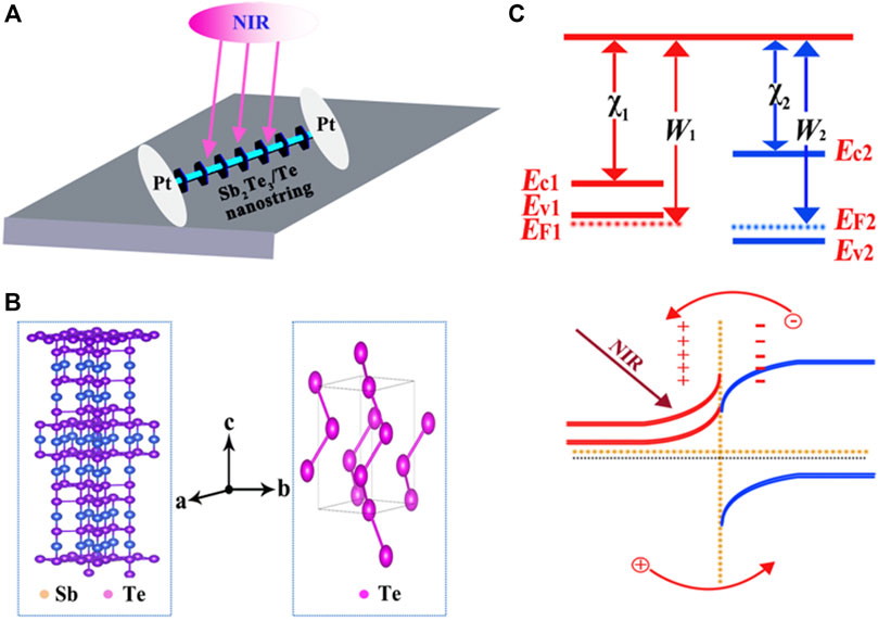
FIGURE 1. (A) Schematic illustration of the Sb2Te3/Te nanostring NIR photodetector. (B) Schematic illustration of the crystal structure of the Sb2Te3 nanosheet and Te nanowire. (C) Energy band diagram of the Sb2Te3/Te nanostring photodetector without and with NIR light illumination.
The Sb2Te3/Te nanostrings are characterized by XRD. Figure 2A (turquoise line) shows the XRD pattern of the Sb2Te3/Te nanostrings. All peak positions in Figure 2A are indexed to the rhombohedral Sb2Te3 (JCPDS No. 71-0393) and the hexagonal Te (JCPDS No. 89-4899). The characteristic peaks of Sb2Te3 and Te are exhibited in Figure 2A such as (015), (110), (205), (101), (012), and (110) planes, which suggest that the as-prepared product is composed of rhombohedral Sb2Te3 and hexagonal Te. In addition, the diffraction intensities of Sb2Te3 (006) and (1010) planes are extremely sharp; however, those of the (101) and (107) planes are distinctly weak, showing that the (hk0) planes in the Sb2Te3 nanostructure grew faster than the (hkl, l ≠ 0) planes. Therefore, the Sb2Te3 crystallization is preferentially grown along with the a or b axle instead of the c axle. As a result, ultrathin Sb2Te3 nanosheets can be generated in the final products. It is remarkable that the crystallinity is scored as 91.67% after refining (Supplementary Figure S1).
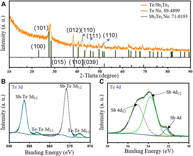
FIGURE 2. (A) X-ray diffraction (XRD) pattern of the Sb2Te3/Te nanostrings. (B,C) XPS spectra of Te (3d) and Sb (4d).
The X-ray photoelectron spectroscopy (XPS) spectra further clarify the structure of Sb2Te3/Te nanostrings. The sharp peaks of Te (3d) and broad peaks of Sb (3d, 4d) can be clearly separated (Supplementary Figure S2). Figures 2B and C reveal that the electron-binding energies of Te 3d3/2 and Te 3d5/2 located at 586.3 eV and at 575.9 eV, respectively, which corresponds to the valence of Sb-Te. The binding energies located at 583.0 and 572.6 eV can be ascribed to the 3d3/2 and 3d5/2 of Te-Te valence. The Raman spectra can also confirm the existence of Te and Sb2Te3. Two typical characteristic peaks are located at 179 and 235 cm−1, which can actually be assigned to Te (Yin et al., 2018) (Supplementary Figure S3). The representative signals of Sb2Te3 are located at 309 and 343 cm−1. All facts confirm that the as-synthesis product exhibits a fine crystallinity with definite constitution and structure.
Figures 3A–C reveal the morphologies of the nanostrings at different magnifications by field-emission scanning electron microscopy (FESEM). The nanostrings are composed of multiple nanosheets that are strung together through the center by Te nanowires. The length of the Te nanostructure is approximately 10 μm (Supplementary Figure S4), which is beneficial for the photodetection device fabrication by conventional photolithography. Figure 3D demonstrates that the Sb2Te3 nanosheets are embedded in the Te nanowire and the diameter is approximately 300 nm. HRTEM pattern analysis effectively indicates the monocrystalline texture of Sb2Te3/Te nanostrings (Figures 3E and F). The lattice fringes are noticeable and the d-spacings are 0.2375 and 0.25 nm, which correspond well to the Tellurium (012) and Sb2Te3 (110) lattice planes, respectively. The selected area electron diffraction (SAED) pattern (Supplementary Figure S5) is well indexed to the hexagonal phase of Tellurium, and corresponding to the diffraction peaks of (012), (101), and (110) planes shown in the XRD pattern. Energy dispersive spectrometer (EDS) spectra confirmed that the nanostrings are composed of Sb and Te elements (Figures 3G–I). Figures 3G–I exhibit the TEM elemental mapping images of the Sb2Te3/Te nanostring, which further confirms that the as-prepared product is only composed of Te and Sb elements.
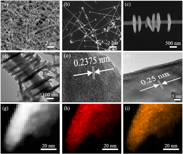
FIGURE 3. (A–C) SEM images of the Sb2Te3/Te nanostrings at different magnifications. (C) TEM image of the Sb2Te3/Te nanostrings. (D) TEM image of the Sb2Te3/Te nanostrings. (E,F) HRTEM images of the Sb2Te3/Te nanostrings (G–I) and elemental mapping images of Sb2Te3/Te nanostrings.
The temperature-dependent current-voltage (I-V) curves of the as-fabricated device are studied to disclose its electrical transportation characteristics. Figures 4A and B demonstrate the I-V characteristics from 10 to 300 K in the dark and under 980 nm light illumination (0.5 mW cm−2). The dark current increases with falling temperature. This can be attributed to the unique electronic construction, particularly when the Fermi level is close to the Dirac point. The I-V curves are virtually linear when illuminated by 980 nm light and show that the Te nanowire and Pt-Ti/Au electrode can form a contact form with Ohmic contact.
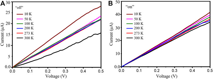
FIGURE 4. I-V curves of the Sb2Te3/Te nanostrings in the dark (A) and under illumination (B) at various temperatures from 10 to 300 K.
Considering the temperature-dependent electrical properties of the Sb2Te3/Te nanostrings, the photoresponse characteristics at different temperatures were studied. Figure 5 shows the temporal photoresponse properties of the device at 10K, 50K, 100K, 200K, 273K, and 300K with periodic irradiation of 980 nm at a bias voltage of 1 V. The figure shows that when the bias voltage is kept unchanged, the change of the current is consistent with the changes of the temperatures. The dark current can decrease to the lowest value of 8.5 μA at 100K and the photocurrent can reach its highest value of 79.5 μA at 10K under the 1 V bias voltage and on/off illumination of 980 nm light. Additionally, the photoresponse characteristics of the as-constructed photodevice are homologous at temperatures of 273 and 300 K due to the temperature effect (Qi et al., 2018). The optical switching behavior of this photodetector is highly reversible with good stability and reproducibility. There is no significant degradation in its switching behavior even after multiple periodic optical switching changes. It is worth noting that different from the conventional photodetectors with a very fast response speed based on semiconductor nanostructures, the as-fabricated device has a moderately (several hundred seconds) slow rising and falling time (Cai et al., 2022). The difference in the response speed is possible due to their distinction of the band structures.
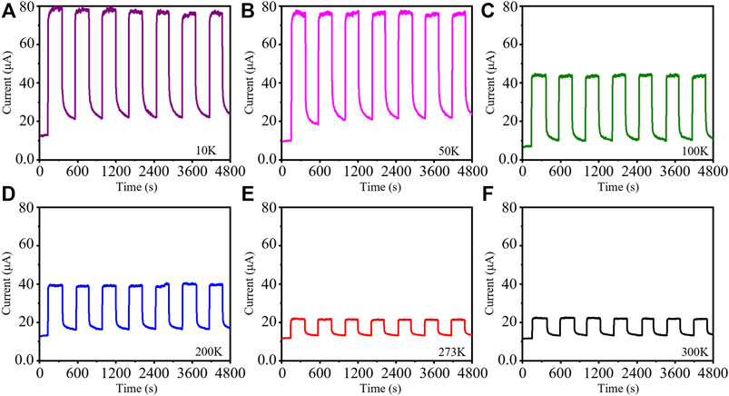
FIGURE 5. Time-resolved photoresponse of the Sb2Te3/Te nanostring photodetector under different temperatures at 1 V bias voltage: (A) 10 K, (B) 50 K, (C) 100 K, (D) 200 K, (E) 273 K, and (F) 300 K.
The responsivity ® and detectivity (D*) are also two key index factors of photodetectors. “R” is the photocurrent per unit incident light power on the calculating device, which can reflect the sensitivity of the device to the intensity of incident light. “D*” shows the performance of detecting weak light (Yu et al., 2018). These two key parameters can be derived according to the following equations:
where Iph is the photocurrent, Id is the dark current, P is the incident light power density (0.5 mW cm2), S is the effective area of the device receiving light (∼1.5 × 10⁻⁸ cm2), and e is the fundamental charge (1.6 × 10⁻¹⁹ C) (Xu et al., 2022; Zhang et al., 2022). According to Eqs 1, 2, the “R” and “D*” of the detector under 3 V bias voltage and different illumination intensities are shown in Figure 6. The results show that the detector has a photoresponsive®(R) of approximately 9.5 × 10¹¹ μA W−1 and a detectable rate (D*) of approximately 1.3×10¹⁷ Jones under 1 V bias voltage and 50 K with the light irradiation of 980 nm.
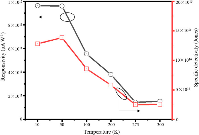
FIGURE 6. Responsivity (R) and detectivity (D*) of a selenium self-supporting film photodetector under different light intensities.
Conclusion
We report a near NIR photodetector based on a topological insulator antimony telluride (Sb2Te3) and tellurium (Te) heterostructure, which are prepared by controllable hydrothermal and photolithography methods. The elaborately constructed device exhibits topological insulator properties, and the resistance especially decreases with increasing temperature in the range of 10–300 K. Further optoelectronic characterization shows that the as-fabricated photodetector delivers obvious sensitivity to 980 nm light illumination. The performance of responsivity and detectivity are remarkable and are much better than those of other Te-based topological insulator photodetector devices. The research suggests that the as-constructed NIR photodetector may have great potential in low-temperature optoelectronic devices.
Data availability statement
The datasets presented in this study can be found in online repositories. The names of the repository/repositories and accession number(s) can be found at: https://www.ccdc.cam.ac.uk/structures/- 2211392 and 2211393.
Author contributions
All authors listed have made a substantial, direct, and intellectual contribution to the work and approved it for publication.
Funding
This work was financially supported by the National Natural Science Foundation of China (Nos. 52171207, 52271211, 52072120, and 52204311), HORIZON- Marie Skłodowska-Curie Actions-2021-PF (No. 101065098), the Hunan Provincial Natural Science Foundation of China (Nos. 2022JJ40162 and 2022JJ40159), the Scientific Research Fund of Hunan Provincial Education Department, China (Nos. 21B0406 and 21B0591), and the Scientific and Technological Project of Yueyang City.
Conflict of interest
The authors declare that the research was conducted in the absence of any commercial or financial relationships that could be construed as a potential conflict of interest.
Publisher’s note
All claims expressed in this article are solely those of the authors and do not necessarily represent those of their affiliated organizations or those of the publisher, the editors, and the reviewers. Any product that may be evaluated in this article, or claim that may be made by its manufacturer, is not guaranteed or endorsed by the publisher.
Supplementary material
The Supplementary Material for this article can be found online at: https://www.frontiersin.org/articles/10.3389/fchem.2022.1060523/full#supplementary-material
References
Cai, Y., Hou, T.-T., Wang, C.-Y., Tang, Y.-H., Zhang, Z.-Y., Zhang, D., et al. (2022). Fluorescence enhancement of dicyanomethylene-4H-pyran derivatives in solid state for visualization of latent fingerprints. Front. Chem. 10, 943925. doi:10.3389/fchem.2022.943925
Chen, G., Dresselhaus, M. S., Dresselhaus, G., Fleurial, J. P., and Caillat, T. (2003). Recent developments in thermoelectric materials. Int. Mat. Rev. 48 (1), 45–66. doi:10.1179/095066003225010182
Cheng, L., Chen, Z.-G., Yang, L., Han, G., Xu, H.-Y., Snyder, G. J., et al. (2013). T-shaped Bi2Te3-Te heteronanojunctions: Epitaxial growth, structural modeling, and thermoelectric properties. J. Phys. Chem. C 117 (24), 12458–12464. doi:10.1021/jp4041666
Cozzoli, P. D., Pellegrino, T., and Manna, L. (2006). Synthesis, properties and perspectives of hybrid nanocrystal structures. Chem. Soc. Rev. 35 (11), 1195–1208. doi:10.1039/b517790c
Dong, G.-H., Zhu, Y.-J., and Chen, L.-D. (2010). Microwave-assisted rapid synthesis of Sb2Te3 nanosheets and thermoelectric properties of bulk samples prepared by spark plasma sintering. J. Mat. Chem. 20 (10), 1976–1981. doi:10.1039/b915107a
Duan, T., Liao, C., Chen, T., Yu, N., Liu, Y., Yin, H., et al. (2015). Single crystalline nitrogen-doped InP nanowires for low-voltage field-effect transistors and photodetectors on rigid silicon and flexible mica substrates. Nano Energy 15, 293–302. doi:10.1016/j.nanoen.2015.05.002
Fu, L., Kane, C. L., and Mele, E. J. (2007). Topological insulators in three dimensions. Phys. Rev. Lett. 98 (10), 106803. doi:10.1103/physrevlett.98.106803
Ikeda, T., Collins, L. A., Ravi, V. A., Gascoin, F. S., Haile, S. M., and Snyder, G. J. (2007). Self-assembled nanometer lamellae of thermoelectric PbTe and Sb2Te3 with epitaxy-like interfaces. Chem. Mat. 19 (4), 763–767. doi:10.1021/cm062121p
Jiang, J., Chen, L., Bai, S., Yao, Q., and Wang, Q. (2005). Thermoelectric properties of p-type (Bi2Te3)x (Sb2Te3)1− x crystals prepared via zone melting. J. Cryst. Growth 277 (1-4), 258–263. doi:10.1016/j.jcrysgro.2004.12.144
Jin, C., Zhang, G., Qian, T., Li, X., and Yao, Z. (2005). Large-area Sb2Te3 nanowire arrays. J. Phys. Chem. B 109 (4), 1430–1432. doi:10.1021/jp046100z
Lee, J. S., Brittman, S., Yu, D., and Park, H. (2008). Vapor-liquid-solid and vapor-solid growth of phase-change Sb2Te3 nanowires and Sb2Te3/GeTe nanowire heterostructures. J. Am. Chem. Soc. 130 (19), 6252–6258. doi:10.1021/ja711481b
Li, Z., Zheng, S., Zhang, Y., Chen, H., Huang, T., and Lu, G. (2015). High-yield synthesis, controllable evolution, and thermoelectric properties of Te/Bi2Te3 heterostructure nanostrings. J. Electron. Mat. 44 (6), 2061–2067. doi:10.1007/s11664-015-3656-1
Matsunaga, T., Kojima, R., Yamada, N., Kifune, K., Kubota, Y., Tabata, Y., et al. (2006). Single structure widely distributed in a GeTe-Sb2Te3 pseudobinary system: A rock salt structure is retained by intrinsically containing an enormous number of vacancies within its crystal. Inorg. Chem. 45 (5), 2235–2241. doi:10.1021/ic051677w
Matsunaga, T., Yamada, N., and Kubota, Y. (2004). Structures of stable and metastable Ge2Sb2Te5, an intermetallic compound in GeTe-Sb2Te3 pseudobinary systems. Acta Crystallogr. B 60 (6), 685–691. doi:10.1107/s0108768104022906
Pradhan, A., Roy, A., Tripathi, S., Som, A., Sarkar, D., Mishra, J. K., et al. (2017). Ultra-high sensitivity infra-red detection and temperature effects in a graphene-tellurium nanowire binary hybrid. Nanoscale 9 (27), 9284–9290.
Qi, J., Ma, N., Ma, X., Adelung, R., and Yang, Y. (2018). Enhanced photocurrent in BiFeO3 materials by coupling temperature and thermo-phototronic effects for self-powered ultraviolet photodetector system. ACS Appl. Mat. Interfaces 10 (16), 13712–13719. doi:10.1021/acsami.8b02543
Sosso, G., Caravati, S., and Bernasconi, M. (2009). Vibrational properties of crystalline Sb2Te3 from first principles. J. Phys. Condens. Matter 21 (9), 095410. doi:10.1088/0953-8984/21/9/095410
Sun, H., Jiang, T., Zang, Y., Zheng, X., Gong, Y., Yan, Y., et al. (2017). Broadband ultrafast photovoltaic detectors based on large-scale topological insulator Sb2Te3/STO heterostructures. Nanoscale 9 (27), 9325–9332.
Tominaga, J., Fons, P., Kolobov, A., Shima, T., Chong, T. C., Zhao, R., et al. (2008). Role of Ge switch in phase transition: Approach using atomically controlled GeTe/Sb2Te3 superlattice. Jpn. J. Appl. Phys. (2008). 47 (7S1), 5763–5766. doi:10.1143/jjap.47.5763
Tominaga, J., Kolobov, A., Fons, P., Nakano, T., and Murakami, S. (2014). Ferroelectric order control of the Dirac-semimetal phase in GeTe-Sb2Te3 superlattices. Adv. Mat. Interfaces 1 (1), 1300027. doi:10.1002/admi.201300027
Wang, Y.-L., Luo, T., Zhang, J., Fan, C., Li, X., Li, C., et al. (2022). AIE-based fluorescent micro-optical sectioning tomography for automatic 3D mapping of β-amyloid plaques in Tg mouse whole brain. Chem. Eng. J. 446, 136840. doi:10.1016/j.cej.2022.136840
Wesolowski, A., Stresman, G., Eagle, N., Stevenson, J., Owaga, C., Marube, E., et al. (2014). Quantifying travel behavior for infectious disease research: A comparison of data from surveys and mobile phones. Sci. Rep. 4, 5678. doi:10.1038/srep05678
Xia, Y., Qian, D., Hsieh, D., Wray, L., Pal, A., Lin, H., et al. (2009). Observation of a large-gap topological-insulator class with a single Dirac cone on the surface. Nat. Phys. 5 (6), 398–402. doi:10.1038/nphys1274
Xu, T., Yin, H., Yu, P., He, Z., Chen, N., Shen, W., et al. (2022). Ultraviolet photodetectors based on dimetallofullerene Lu2@Cs(6)-C82 nanorods. ACS Appl. Nano Mat. 5 (1), 1683–1689. doi:10.1021/acsanm.1c04497
Yang, J., Aizawa, T., Yamamoto, A., and Ohta, T. (2000). Thermoelectric properties of p-type (Bi2Te3)x(Sb2Te3)1-x prepared via bulk mechanical alloying and hot pressing. J. Alloys Compd. 309 (1-2), 225–228. doi:10.1016/s0925-8388(00)01063-x
Yin, H., Yu, X.-X., Yu, Y.-W., Cao, M.-L., Zhao, H., Li, C., et al. (2018). Tellurium nanotubes grown on carbon fiber cloth as cathode for flexible all-solid-state lithium-tellurium batteries. Electrochim. Acta 282, 870–876. doi:10.1016/j.electacta.2018.05.190
Yu, X.-X., Yin, H., Li, H.-X., Zhang, W., Zhao, H., Li, C., et al. (2017). Piezo-phototronic effect modulated self-powered UV/visible/near-infrared photodetectors based on CdS:P3HT microwires. Nano Energy 34, 155–163. doi:10.1016/j.nanoen.2017.02.033
Yu, X.-X., Yin, H., Li, H.-X., Zhao, H., Li, C., and Zhu, M.-Q. (2018). A novel high-performance self-powered UV-vis-NIR photodetector based on a CdS nanorod array/reduced graphene oxide film heterojunction and its piezo-phototronic regulation. J. Mat. Chem. C 6 (3), 630–636.
Zhang, H., li, L., Zheng, D.-s., Xiong, Y., Yu, C., Yin, H., et al. (2022). Broadband photodetector based on vapor-deposited selenium self-supporting films. Ceram. Int. 48 (19), 27750–27757. doi:10.1016/j.ceramint.2022.06.075
Zheng, K., Luo, L.-B., Zhang, T.-F., Liu, Y.-H., Yu, Y.-Q., Lu, R., et al. (2015). Optoelectronic characteristics of a near infrared light photodetector based on a topological insulator Sb2Te3 film. J. Mat. Chem. C 3 (35), 9154–9160. doi:10.1039/c5tc01772f
Keywords: photodetector, responsivity and detectivity, low-temperature, heterojunction, epitaxial growth
Citation: Yin H, Li H, Yu X-x and Cao M (2022) Design of Sb2Te3 nanoblades serialized by Te nanowires for a low-temperature near-infrared photodetector. Front. Chem. 10:1060523. doi: 10.3389/fchem.2022.1060523
Received: 03 October 2022; Accepted: 21 October 2022;
Published: 18 November 2022.
Edited by:
Hailong Wang, Ningxia University, ChinaCopyright © 2022 Yin, Li, Yu and Cao. This is an open-access article distributed under the terms of the Creative Commons Attribution License (CC BY). The use, distribution or reproduction in other forums is permitted, provided the original author(s) and the copyright owner(s) are credited and that the original publication in this journal is cited, in accordance with accepted academic practice. No use, distribution or reproduction is permitted which does not comply with these terms.
*Correspondence: Minglei Cao, cml07114052@163.com