1. Introduction
The optimal use of diverse renewable energy sources is one of the main challenges in terms of power and energy. In order to connect renewable energy sources (RESs) to the network, the use of electronic power interfaces is essential. Solar cell systems are one of the most desirable renewable energy sources due to the availability of solar radiation and flexibility in installing panels. It is preferable to use modular photovoltaic systems to increase the efficiency of these panels and to overcome problems such as shadowing on panels and mismatches between them [
1,
2]. In these systems, a high-efficiency DC–DC converter is used to increase the output voltage of the photovoltaic cells and connect them into the high-voltage bus [
3,
4,
5,
6]. Additionally, these batches are used in many applications including emergency electrical systems, fuel cells, server power supplies, and high-intensity discharge lamps [
7].
Boost converters can be divided into isolated and non-isolated categories. Isolated converters can usually present low amounts of efficiency. In these types of choppers, the high voltage gain is obtained through adjustment of the correct transformer ratio. Non-isolated converters are highly applicable structures due to their high efficiency, high power density, and low cost in medium and low power systems [
8]. In [
9], a three-level boost converter was introduced. This converter can reduce the voltage stress of semiconductor components when compared to a conventional boost converter, which is suitable for high voltage applications. As a result, switching losses and electromagnetic interference (EMI) are improved due to low voltage stress in this configuration. Nevertheless, semiconductor parts act under hard switching conditions and the problem of recovering the output diode is one of the most serious problems in this type of converter.
In [
10,
11], a highly addictive coupled-inductor single-switch converter was introduced. In [
10], the leakage energy of the coupled-inductors was reclaimed by the clamp circuit, which reduces the voltage stress on the switch and diodes. As a result, the switch can be used with a low light-up time resistance, which results in improved efficiency. However, it should be noted that this converter has a complex structure. In [
12], an interleaved based configuration by coupled-inductors was introduced. Due to the use of a voltage multiplier and coupled-inductors, a high voltage gain was achieved for the proposed structure. In this converter, due to the use of cross-linked inductors, the input current ripple decreased. Additionally, by using active clamping circuits, the leakage energy of the inductor’s spools and soft-switching conditions were created for the main switches. One of the disadvantages of topologies by coupled-inductor is the high voltage stresses on output diodes that make use of high voltage diode applications and clamper structures. In [
13], a high-gain nonsymmetrical interleaved converter was presented. In this structure, two ferrite cores were used for two inductors. Due to the use of two switches, in addition to reducing the current stress of the switches, the ripple of the input current will be limited. One of the disadvantages of this converter is the creation of hard switching conditions, which increases the number of magnetic elements and the total volume of the circuit.
In [
14], a boost converter integrated with a fly-back topology was introduced to obtain the high voltage gain. In this structure, the boost converter acts like a passive clamp circuit and recycles the leakage energy. In [
15], a similar boost converter was introduced. In this converter, the clamper capacitor is located in the direction of charging the output capacitor, and in addition to absorbing the self-leakage energy, it also increases the voltage gain of the converter. To reduce the number of components, single switch fly-back boost converters are commonly integrated. Different designs of this converter are presented in [
16]. One of the main concerns is the voltage and current spikes on the switching devices in a power module. Zero voltage switching (ZVS), zero current switching (ZCS), zero voltage transition (ZVT), and zero current transition (ZCT) are different approaches that can reduce these stresses and decrease the switching losses on power diodes and power switches [
17,
18]. In these ways, to obtain higher efficiency, applying an additional switch is often inevitable and can need more control topologies and enhance the complexity and cost of the converter.
Cascade structures can be employed for high step-up requirements. The authors in [
19,
20] proposed sample topologies for this kind of converter. Higher DC gains can be achieved by applying more serial blocks of converters, but by increasing the number of blocks, the number of components will increase, especially extra power switches that have been applied, and the dynamic and frequency losses will increase, which will seriously affect the efficiency. Furthermore, the control process will be difficult for more power switches and the total cost will increase. Our study introduces a topology that can provide a pre-amplifier block containing an inductor, two power diodes, and a capacitor. This configuration can increase the input voltage, and according to the duty ratio, this amount can be greater. Next, it acts as a boost converter and increases the voltage to higher values. For high efficiency purposes, the diodes on the pre-amplifier part act in a complementary manner and when one of them is in ON mode, another is in OFF mode and vice versa. So, in comparison with a classical cascaded boost converter, the proposed configuration is more efficient. All mathematical analysis of the projected converter, calculations of the voltage gain, and the controller design and small signal analysis based on steady space matrixes are presented in
Section 2.
Section 3 presents the simulation results and the implemented prototype and the performance assessment of the proposed simple controller is presented in
Section 4.
2. Modified Boost Converter (MBC)
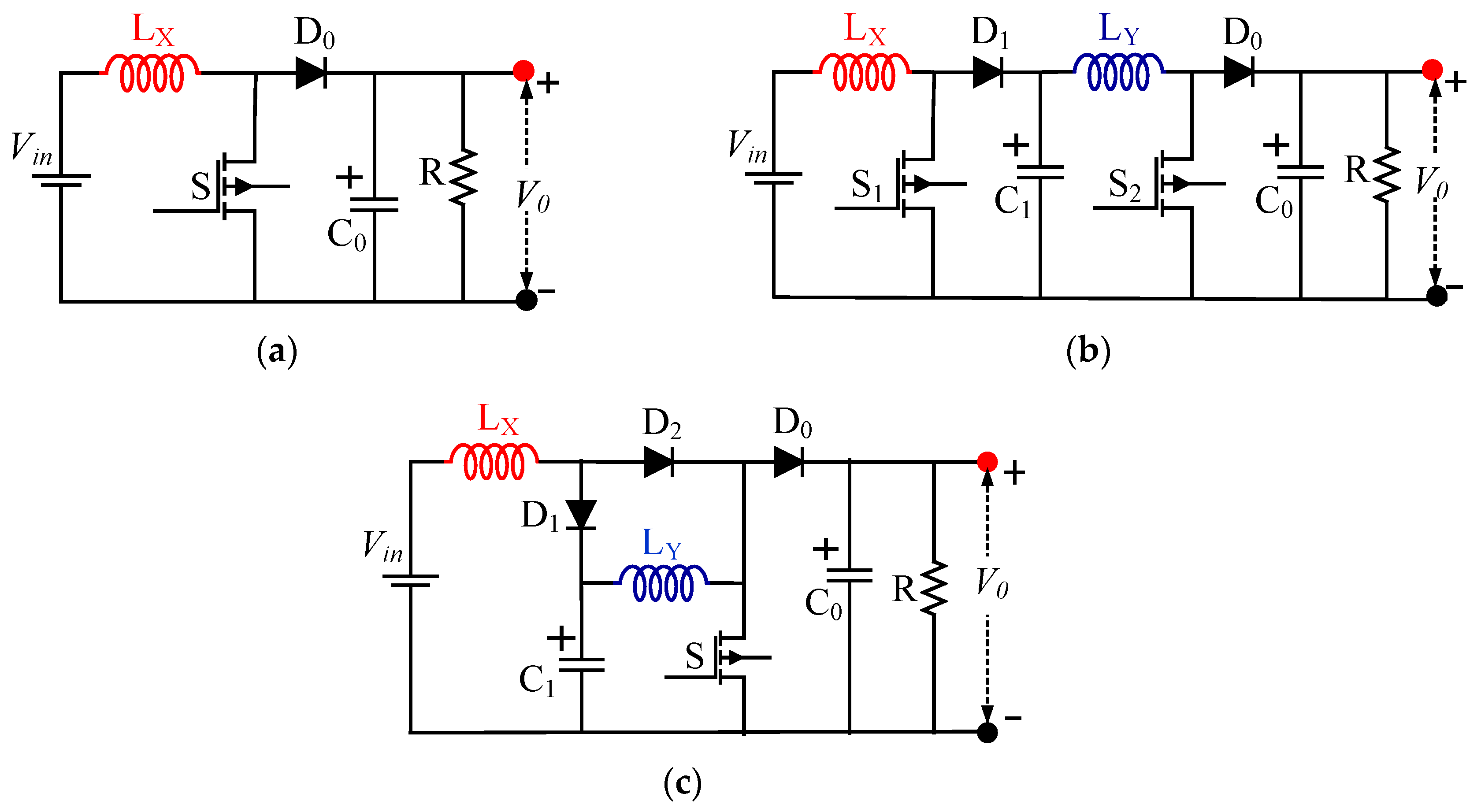
Figure 1a–c shows the conventional, cascaded, and proposed boost converters, respectively. As can be seen in
Figure 1c, a boosting structure is located between the entrance inductor and the power switch. Based on switch ON or OFF working modes, only one of the
D1 and
D2 diodes will be active in the structure and in this way, it makes a preamplifier layer for boosting purposes. All working principles and mathematical analyses have been stipulated for both ON and OFF states of the power switch.
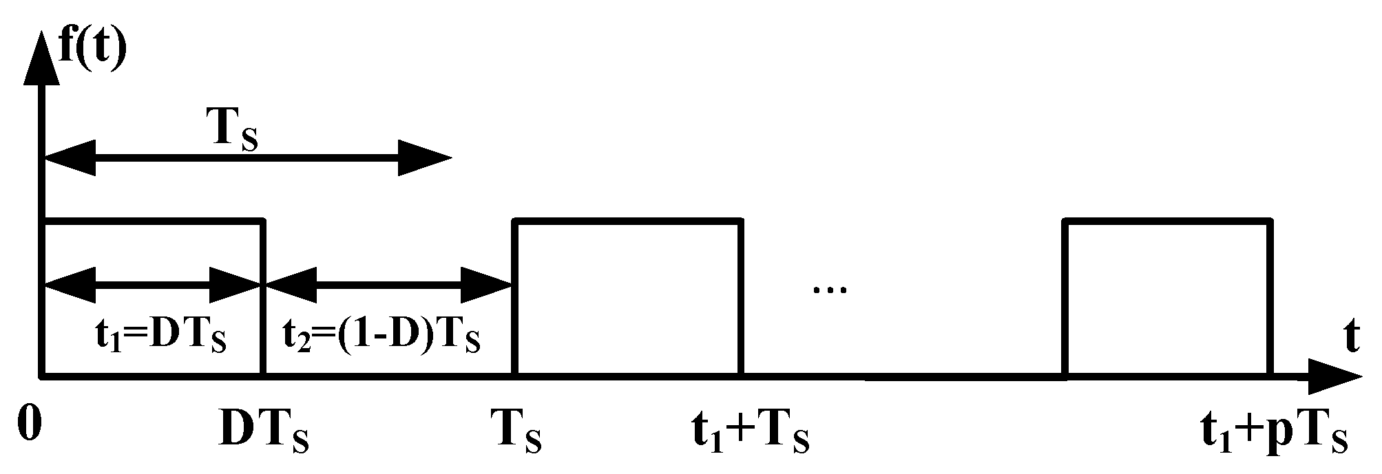
Figure 2 presents the Pulse Width Modulation (PWM) wave applied to the power switch in the boost converter. In this figure for the [0, t
1] and [t
1, T
S] time intervals switch S
1 is in ON and OFF modes, respectively. So, if we consider [0, t
1] interval as DT
S, the [t
1, T
S] interval will be (1-D) T
S. In other words, D is the duty cycle of power switch S
1.
2.1. Converter Analysis
This part presents the converter’s reactions for the ON and OFF time intervals.
2.1.1. Mode-I
For a time-interval that the power switch receives the pulse and is in the short circuit state, both
LX and
LY are magnetizing. This is done by inputting the voltage through diode
D2 and the power switch for
LX and from
C1 and switch for
LY. As can be seen in this mode,
D1 is in mode-I. Based on this statement, currents of inductors are rising in the ON state. As predicted, the voltage value on capacitor
C1 is discharging on
LY through the power switch and decreases. Additionally, the voltage on the output capacitor is discharging on the output load in this mode. The current value of diode
D1 is zero and because of the conducting condition for diode
D2, its current will increase.
Figure 3a shows the ON state of the power switch in the projected structure and
Figure 3b illustrates the simplified form of
Figure 3a.
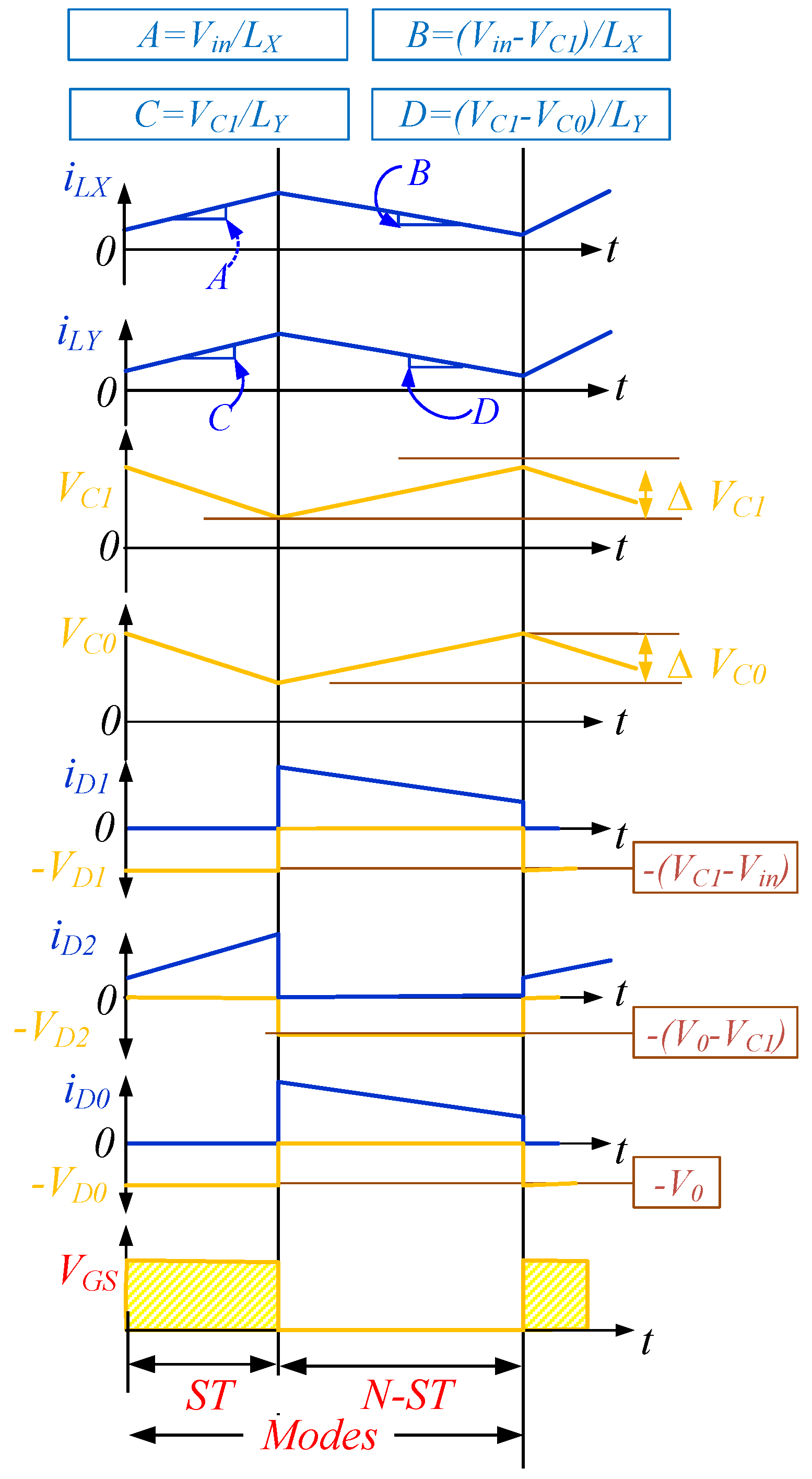
Based on these situations, the current waveform passing through inductor
LX can be written as below:
The current of inductor
LY is:
The voltage waveform for capacitor
C1 can be gained as:
Finally, we can find the voltage for the output capacitor as Equation (4):
The steady-space matrix of the ON state for the proposed converter can be obtained by Equation (5)
2.1.2. Mode-II
In this time interval,
LX is demagnetizing on capacitor
C1 through
D1 and
D2 is in OFF mode. Additionally, inductor
LY is demagnetizing through diode
D0 on the output capacitor and load. In this time interval, as above-mentioned, the voltage values on capacitors
C1 and
C2 will increase through
LX and
LY, respectively.
Figure 4 illustrates all of the components’ conductions in both ON and OFF modes of power Metal Oxide Semiconductor Field Effect Transistor (MOSFET). Small signal analysis for this state was also analyzed and written below. Inductor
LX can be calculated as:
Additionally, the current waveform of inductor
LY is equal with:
The voltage waveform for capacitor
C1 and
C0 are:
Term (1 − d) in the above equations guarantees work in the OFF state. Through the same method, we can obtain the below matrix for the OFF state of the power switch:
So, for both ON and OFF states of the switch, by adding Equations (5) and (10), we have:
For the modeling process of a power circuit by the steady space method, we can find the relation between inputs, outputs, and the current and voltage derivations for the inductors and capacitors by Equation (12):
where
X is the inductor current or capacitor voltage derivate matrix and
C is the coefficient matrix;
u is the input sources matrix; and
D is the coefficient matrix of u. While
Y as the output wave, can be obtained as:
The general view in order to obtain the small signal for the proposed converter can be re-the organized by Equation (14), since
A,
B,
C, and
D can be introduced for the ON and OFF states of power switch:
If we want to introduce the general equation for both ON and OFF states of the power switch through Equation (14), we can obtain:
So, in this condition, the output voltage of the structure can be gained by Equation (16):
The voltage gain of the converter can be found through Equation (17):
2.2. Design of Closed-Loop Controller
By considering that the output voltage of a boost converter should be kept constant by the load or input voltage changes, the key point for controller design is finding an equation between the output voltage and one of the inductor currents or capacitor voltage derivatives and it can be obtained from Equation (9):
Other obtained equations cannot present a direct mathematical relation for the output voltage and Equation (9) is more suitable. Here, the final destination is generating a PWM signal for the power switch that will change according to these amendments to guarantee a fixed output voltage. In Equation (18), u is the PI controller output signal and d is the duty cycle of PWM, which will be implemented to power MOSFET. Equation (18) can be rewritten in a simpler way as:
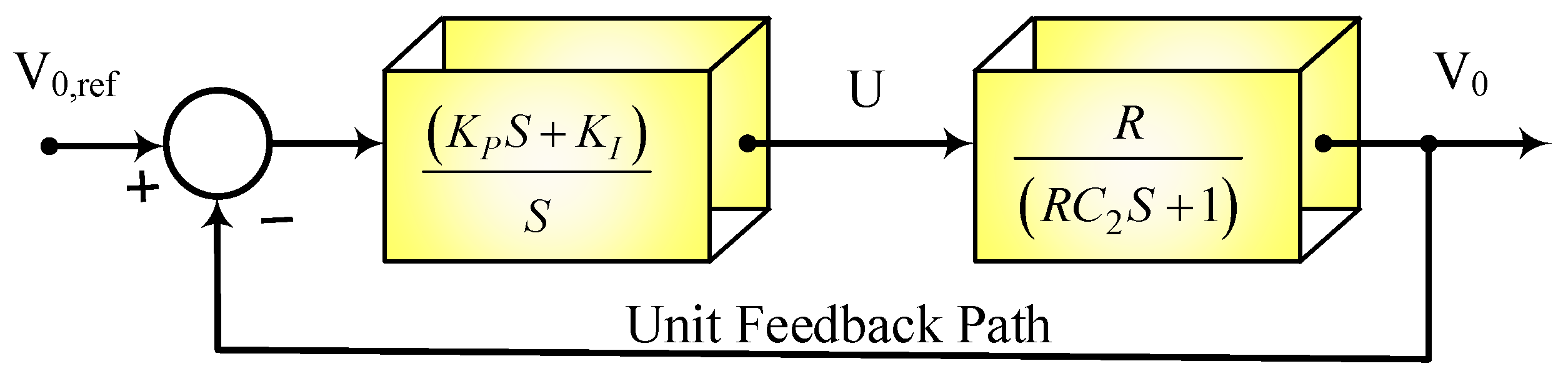
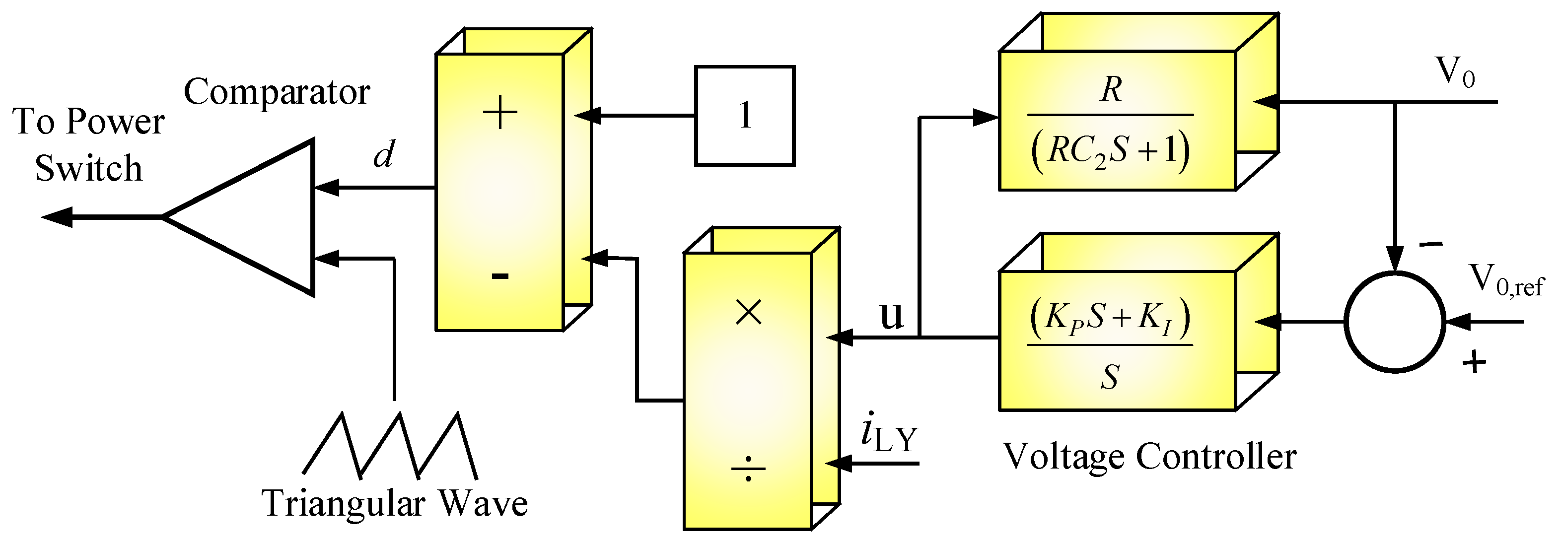
Figure 5 illustrates the closed-loop form of the PI controller based on Equation (18). Since the goal is receiving a fixed DC voltage at the endpoints of the converter on the load side, a sampling of this voltage was done and compared with a reference voltage in order to be applicable by a microcontroller. Therefore, the sampled voltage should be at a comparable level of the reference voltage. For example, for a 120 V as the fixed output voltage, if the reference voltage chosen is 4 V, the sampled voltage should be decreased through high resistors and be equal to 4 V. For other amounts of the output voltage above or under the 120 V, this sampled voltage will change between 3 to 5 V to be comparable with the reference voltage. After passing through the controller, the control signal u will be compared with the current of the second inductor
iLY, and as Equation (19) shows, the desired duty cycle is supplied for the power switch.
Figure 6 presents the controller structure for the proposed converter.
The general form of a PI controller comes from:
where
KP and
KI are the proportional and integral gains of the PI controller. We can put Equation (20) in a feedback loop by a PI controller as presented in
Figure 5 and
Figure 6 by considering Equation (19). The transfer function of closed-loop form of this feedback is equal with:
KP and
KI are the proportional and integral coefficients of the PI controller. It is easy to gain:
The representation of the frequency domain in the kp and ki plane can be introduced by:
By solving this equation for
ω ≠ 0;
For
ω0 = 0, Equation (24) will result in:
For this equation, it can be found that
KP is an arbitrary factor while
KI (0,
θA,
ξ) = 0, unless
XRi(0) =
XIi(0) = 0, which can be possible only under ξ→∞ and Rp(0) = Ip(0) = 0 conditions, which holds by a zero for Gp(S) at the origin. Therefore, damping factor ξ was selected as 0.707, which can present a good response for the second order circuits [
21]. Since
ω0 is a pulsation, it was chosen as less than the switching frequency ωs to get an appropriate response. Based on [
21], this factor can be introduced as Equation (28):
By decreasing the ωn value, the bandwidth of the control system will reduce and will give the increased dither amplitude attenuation and longer set-up times, enhancing the ωn value above the presented band, and resulting in the poor matching of the linearized model’s response to the actual system. This is due to the effect of sampling on the frequency response of the system. In our calculations, the pulsation frequency was fixed to 230.63 rad/s with the consideration of the calculated Kp and KI values based on Equation (22), and the switching frequency was adjusted to 50 kHz, so ωs = 2πfS is equal to 314 K rad/s.
2.3. Comparison of the Conventional Cascaded and Proposed Converters
The main purpose of this section was a comparison between the inductor currents and capacitor voltage ripples for a classical cascade and our proposed converters.
Table 1 summarizes these equations. In this table,
VC1 and
VC0 are the steady state voltages of the
C1 and
C2 capacitors;
D1 and
D2 are the duty cycles of PWM signals for S
1 and S
2 power MOSFETs of the conventional cascaded boost converter;
D is the duty cycle for the proposed converter’s switch, respectively;
TS is the switching frequency; and
∆iLX and
∆iLY are the current ripples for the inductors
LX and
LY, respectively. Additionally,
I0 is the output current and
Vin is the input voltage of the structures.
By considering the same duty cycle for all switches, the current ripples for inductors were the same for both configurations, while the proposed converter uses only one power switch and has a simpler structure and needs to simple with a one controller topology to guarantee a fixed output voltage at the output of the converter. Part of simulations is presented in
Section 3, and can show the first inductor currents, output diode currents, power switch currents, and the average values of these converters. All results can easily confirm the equations presented in
Table 1.
Table 2 illustrates all of the component conduction and switching losses for both conventional, cascaded, and proposed power boost converters comprehensively. This table was written according to [
22]. In this table, the
Pcon and
Psw are the conductive and switching losses, respectively. For example,
Pcon,D1 is the conductive losses of the power diode
D1 and
Psw,D2 is the switching losses for the diode
D2.
PLX and
PLY are the conductive losses on inductors. Additionally,
Vf is the forward voltage on diodes;
fS is the frequency switching value; and
Qrr1, Qrr2, and
Qrr3 are the electrical charges of the
D1,
D2, and
D0 diode forward capacitors.
TON and
TOFF are presenting the transition times for the power switches for the ON and OFF states, respectively. The dissipated energy for the turn ON and OFF momentary times are presented by
WON and
WOFF.
D’ presents the time that the power switch is in OFF mode.
The main advantage of the proposed converter is that it has only one power switch. Therefore, there are no conductive and switching losses for the second power switch. In addition, it should be considered that it has three power diodes compared with a conventional cascaded converter and the projected converter will have these losses for the third diode. This presents a preferable condition compared with conventional cascaded structures.
2.4. Comparison of the Conventional Cascaded and Proposed Converters
By considering the ideal conditions for all inductors, capacitors, power diodes, and power switches, the voltage gain of the proposed converter can be obtained. Based on the charging and discharging states of inductors, mathematical evaluation for the voltage gain will appear in two different modes.
State 1: Voltage across inductor LX when the power switch is in ON and OFF modes:
The voltage across inductor
LX will be equal with:
In the above equation, D is for a time interval where the switch is in ON mode and (1-D) is for the OFF state of MOSFET.
State 2: Voltage across inductor LY when the power switch is in ON and OFF modes:
The voltage drops can be calculated as Equation (29):
By replacing Equation (28) into Equation (29), the voltage gain of the proposed structure can be calculated:
Therefore, the voltage gain of the proposed structure can be obtained by Equation (32):
Through a simple calculation, the relation between the input and output current values can be calculated as:
For the proposed converter, we can find the values of the inductor currents from the below equations:
So, the oscillation of the current for these inductors can be presented by:
Additionally, the voltage fluctuation for the output capacitor can be presented by Equation (37):
For the simulation and experimental analysis, considered one percent for these oscillations, the values of the inductors and capacitors can be calculated.
3. Simulation Results and Discussion
A group of simulations were performed in MATLAB SIMULINK R2017a for the evaluation and testing of the stability of the proposed circuit. The input voltage for the structure was adjusted between 25 and 45 V based on the panel’s ability to generate voltage according to different temperature and irradiance values. The output load value was chosen between 50 and 200 ohms for an output power limit of around 288 W. Additionally, 50 kHz was considered as the switching frequency. Simulations were done for the duty cycle from 30% to 90% and the results are presented in this section.
Table 3 presents all of the components and parameters that were used in the simulation.
For our tests, we assumed 0.1 Ω for inductors
LX and
LY as their internal resistance. This value of the internal resistance was tested on a real 200 µH inductor in the laboratory. For that, a fixed 0.5 V implemented on the inductor and serial ammeter showed around 5 A as the current.
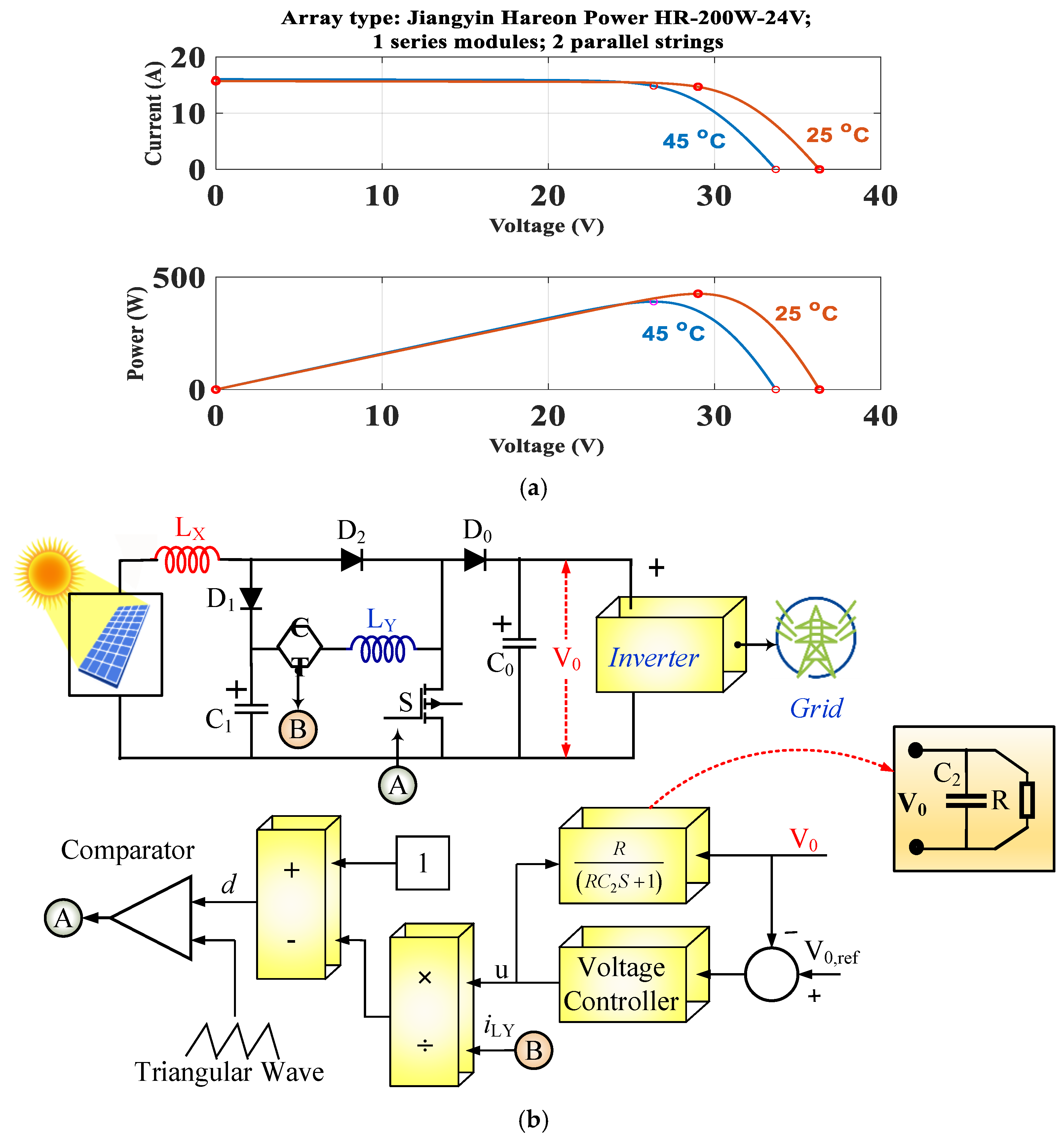
Figure 7a presents the I-V and P-V characteristics of the JIYANGYIN HR-200 W type of the PV array that was selected for hardware implementation. The level of the input voltage and power array were in a good domain of the desired issues presented in
Table 3.
Figure 7b illustrates the final diagram of the proposed converter and controller and as can be seen, a sampling was done based on Equation (9) for the controller design. This diagram is suitable for all kinds of renewable energy sources since these produce limited values of power. The controller loop was drawn based on Equations (18) and (19) and
Figure 5 and
Figure 6. For the controller, PIC18f877 was selected to do the comparison between the reference and sampled voltages and a triangular wave with a 50 kHz frequency was implemented for duty cycle generation to drive the power switch.
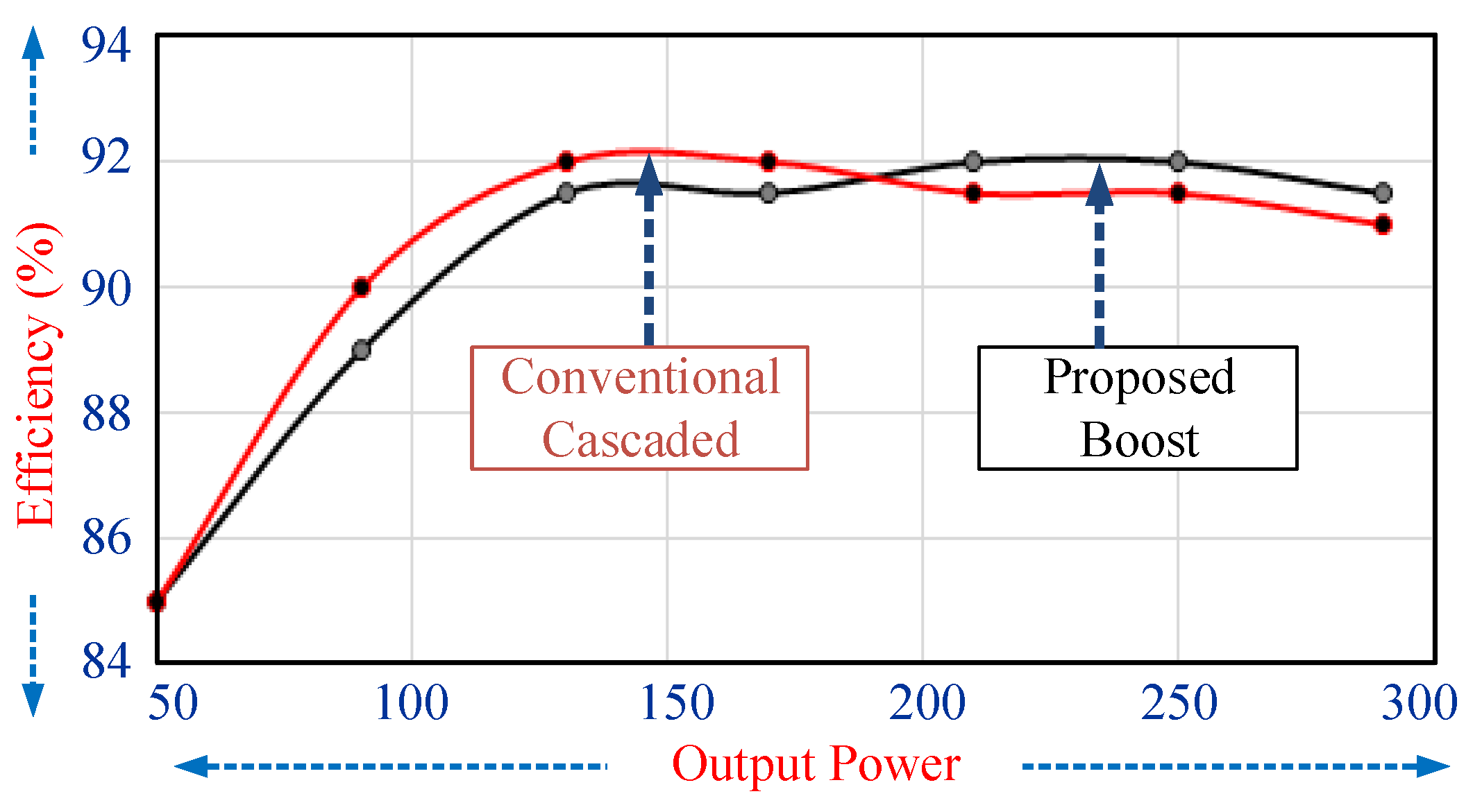
Figure 8 shows the efficiency diagram and was done with a comparison between the conventional cascaded and projected prototypes. The most important reason for the comparable efficiency value for the new converter is its components, especially the power diodes. As mentioned in
Section 2.1, in any time interval of PWM, only one diode will be located in the current direction and will charge the inductors or output capacitor. Additionally, this structure has only one power switch and the same inductor and capacitor values when compared with conventional topologies. As expected, both the proposed and cascaded converters can present low efficiency for lower power based on some fixed losses on devices, and for higher values of power, both structures will be more efficient. By considering that in any time interval two diodes will be active for both topologies by the same number of inductors and since the average current of the proposed converter is approximately equal with the total currents of both MOSFETs of the cascaded converter, efficiency values were obtained close to each other. This figure has been presented for a fixed load with a 200 Ω value and different values of input voltages.
A low-pass filter can be a single-tuned or doubled-tuned filter. This is a technique of eliminating a particular current harmonic by tuning a low-pass filter to a specific frequency that uses low impedance such as 5th multiple or 7th multiple harmonics of the fundamental. High-pass filters on the other hand also consist of passive components with less impedance for harmonics at specific frequencies, thus filtering all harmonics present with higher frequencies [
22]. These filters can be configured as the first order, second order, third order, and fourth-order high pass filters. The first order filters are the simplest form of high-pass filters, containing only one passive component. The order of the high-pass determines the number of component(s) contained in the filter and the higher-order provides better stability to the power system. In our study, we simply applied a capacitor between the PV panel and boost converter. Additionally, the MPPT algorithm of the boost converter helps to decrease the current harmonics of the topology and increase the efficiency.
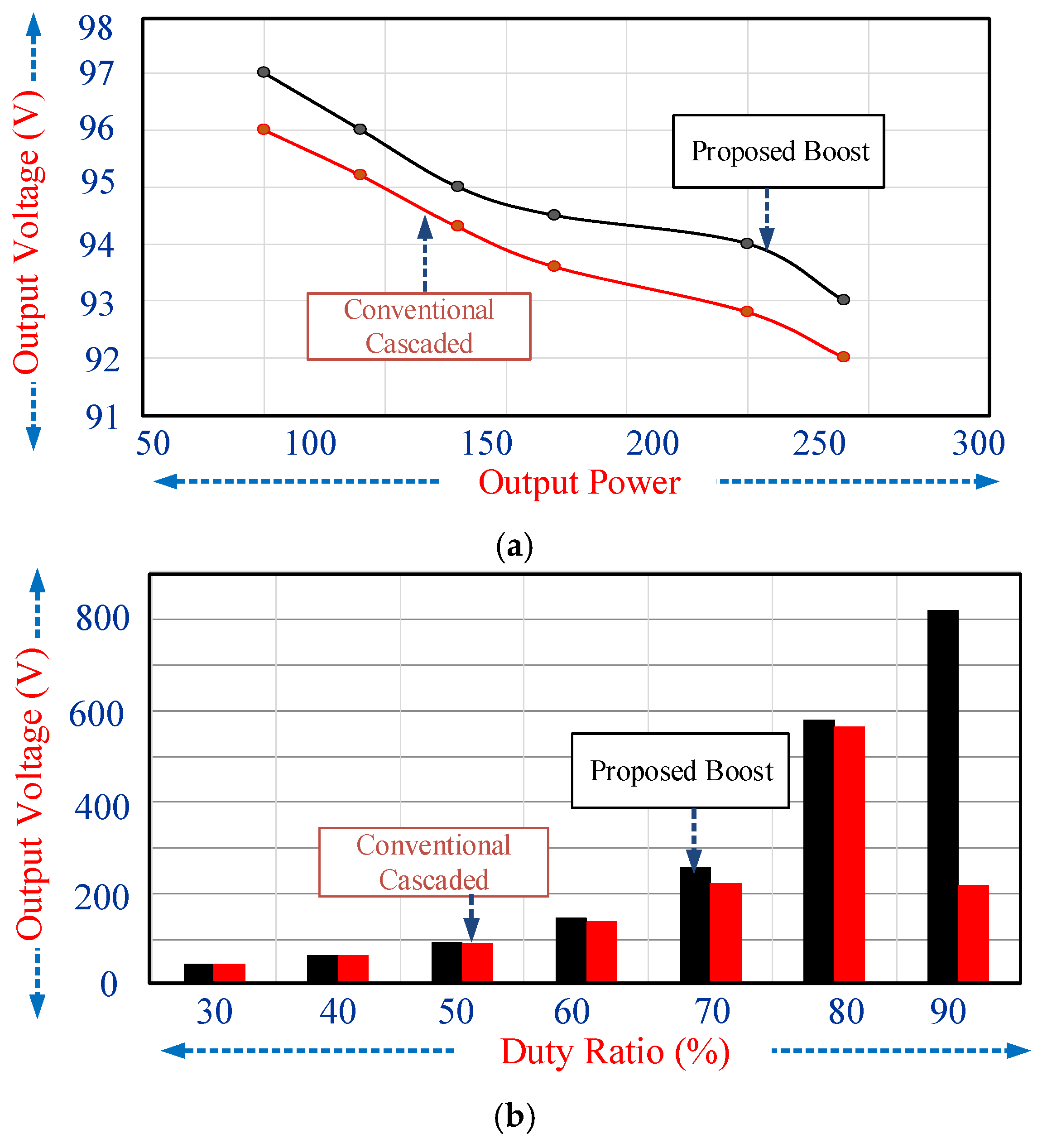
Figure 9a shows the voltage gain for the proposed and conventional boost circuits in 50% of the duty cycle and 50 to 200 Ω as the load. One of the most important issues for a boost converter is the converter’s ability to gain production since voltage transfer is preferred, rather than the current transition in all parts of fossil or renewable energy sources.
The simulation was conducted from 50 W to around 290 W of the output power and for all of this band, the proposed converter presented higher DC gain. Additionally,
Figure 9b illustrates a comparison diagram between the classical cascade and proposed topologies voltage gain for this band of output power for different values of duty cycles from 30 to 90%. The same result is reported for this test.
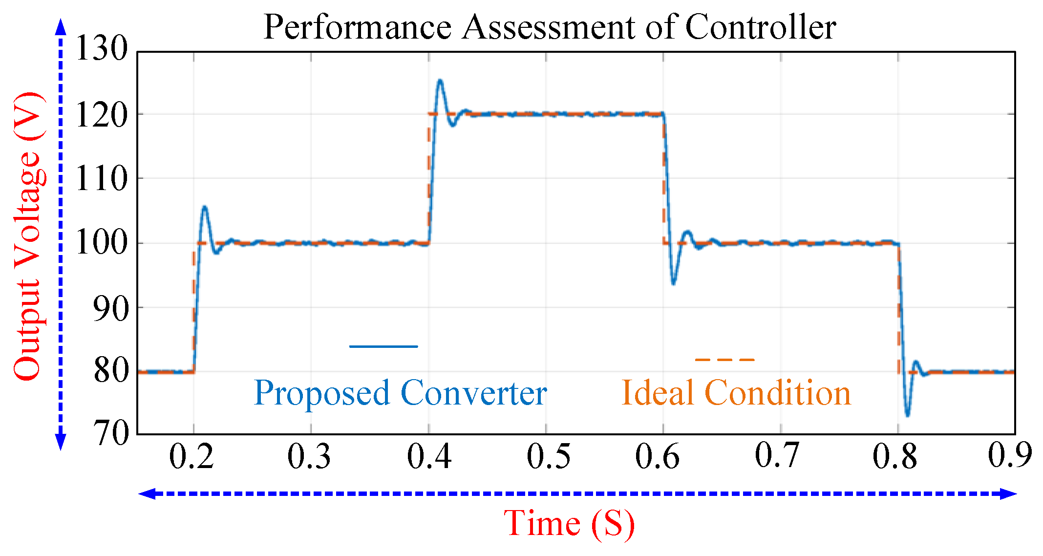
Figure 10 illustrates the controller performance and stability in producing different voltages in output. For this simulation, the input supply was fixed to 24 V and the reference voltage was changed between 80 V, 100 V, and 120 V. For our tests, in order to carry out the PWM implementation to gate-source pins of the power semiconductor switch, the triangle waveform was considered with a 50 kHz frequency. By considering the damping factor for the proposed controller at the change points of the output voltage, a limited value of the overshoot was reported. These overshoot values can have smaller values with PI controller internal adjustments in MATLAB/SIMULINK for the upper and lower output limits, which is applicable for an embedded controller like the M9036A and M9037A or MEC1609 series.
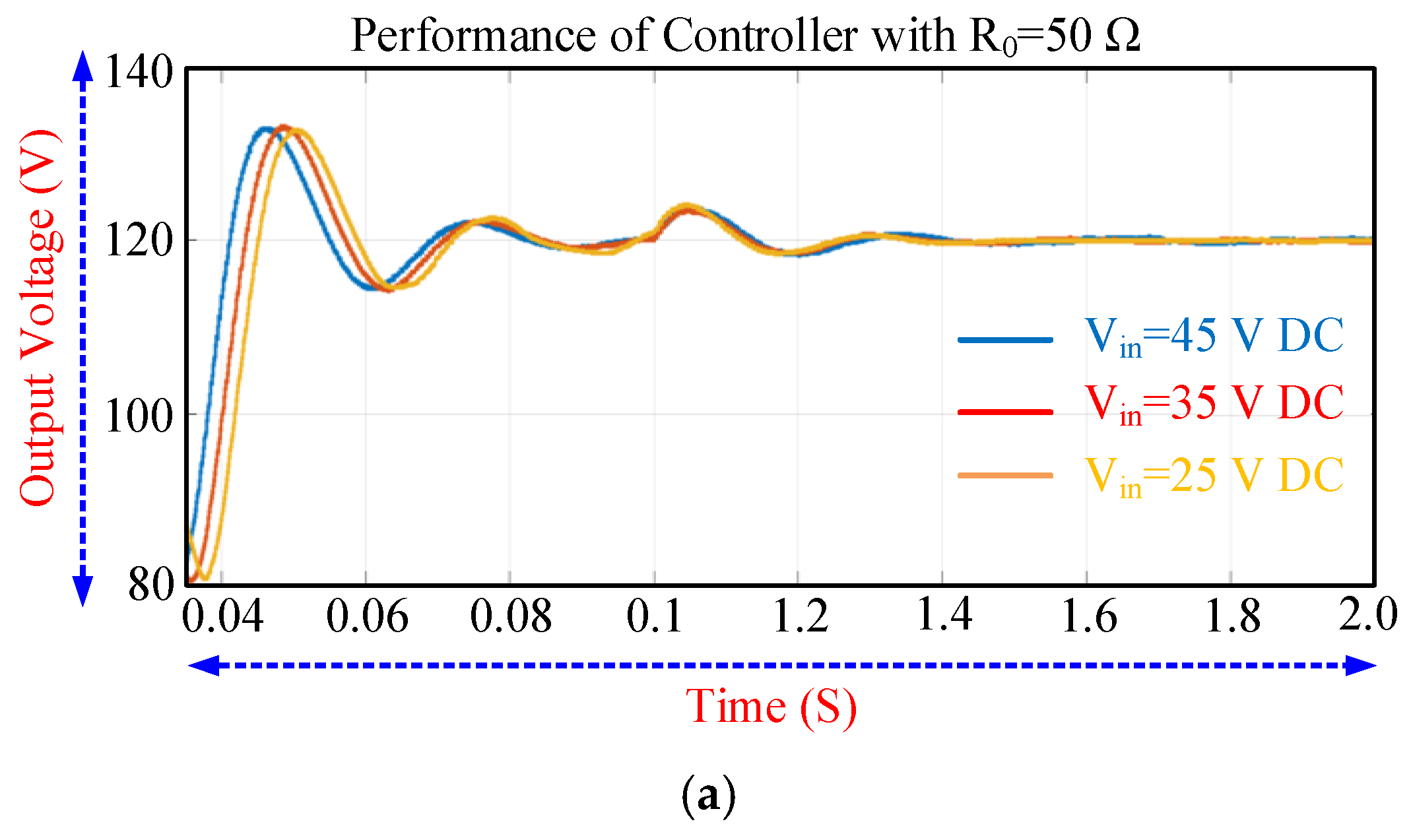
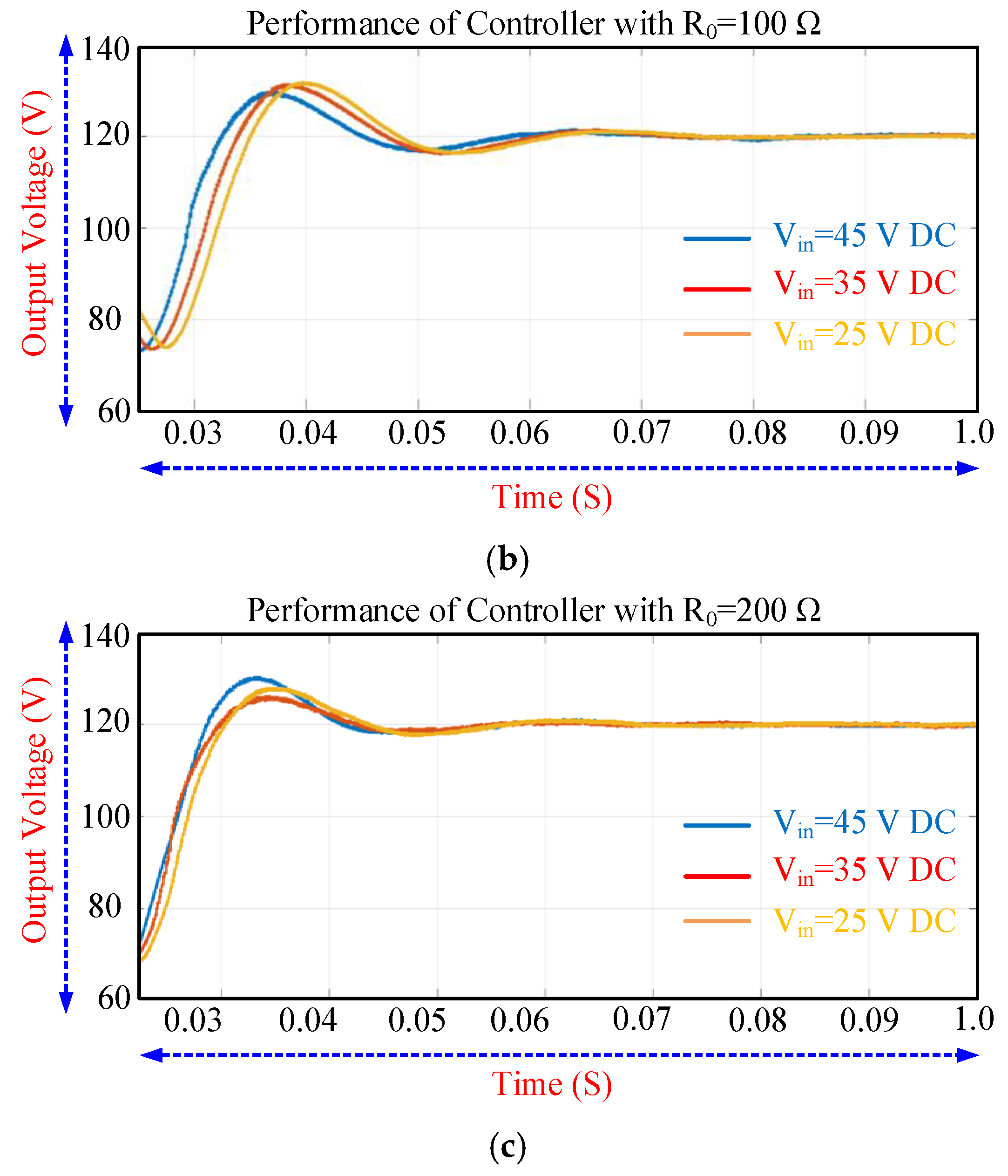
Figure 11 presents the performance of the controller to present the fixed voltage at the load side by changing the input voltage values. As known, PV panels based on different irradiance and temperatures present different values of voltages. Therefore, one of the specifications of a good converter and controller is the ability in obtaining a fixed DC voltage for load by different values of the input voltage. Therefore, in the worst condition, if both the input voltage and output load change, we should consider the performance of the controller for reliability analysis.
Figure 11 presents the reaction of the controller for input voltages from 25 V to 45 V and load values from 50 Ω to 200 Ω. As reported in
Figure 11a, and as expected, for higher loads where higher currents are needed, the overshoot is higher and the settling time is longer. For a higher amount of input voltages and lower amount of output currents, as
Figure 11c presents, both overshoot value and settling time are less. In addition, it can be found that when the input voltage is higher for a fixed load, the overshoot is less and settling time is shorter.
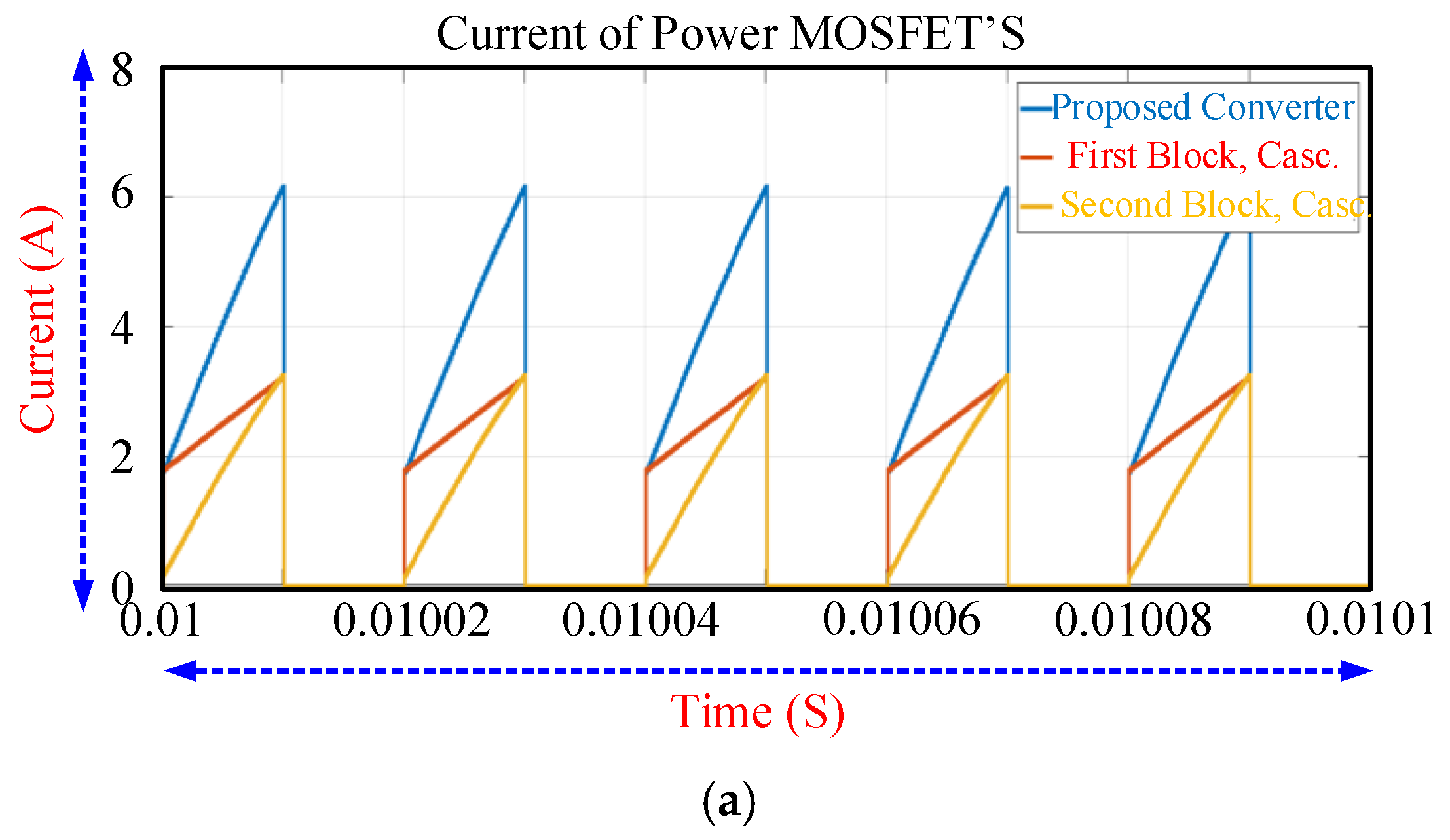
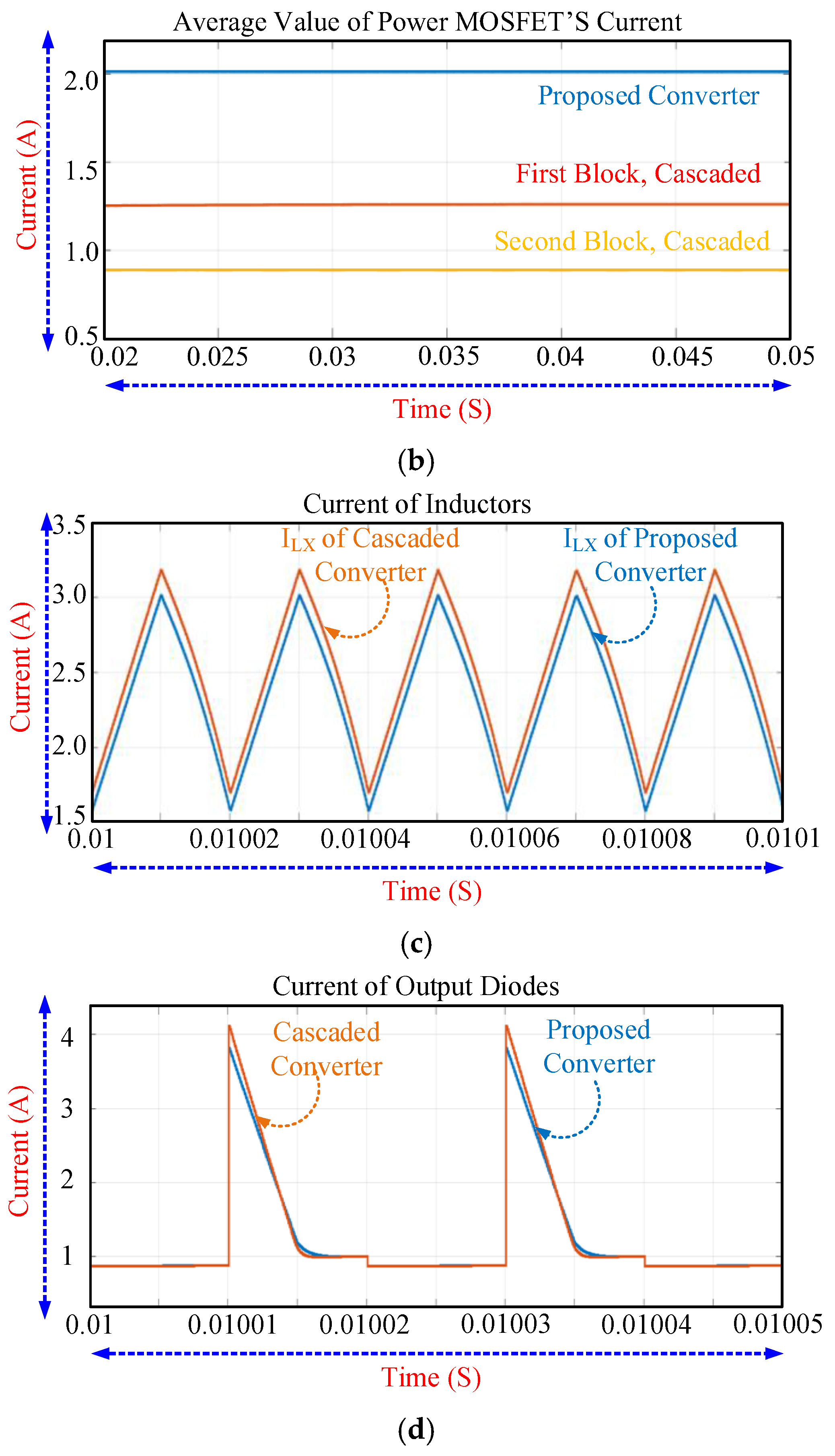
Figure 12 illustrates the current values for the power MOSFETs, output diodes, and input inductors of around 50 W of output power. As can be seen from
Figure 12a,b, approximately the average value of the current for the switch in the proposed converter was equal with the total currents of switches in the cascaded converter. In fact, we should make a trade-off between having two different power MOSFETs with two controller structures and only one power MOSFET with only one controller. Moreover, for the new SiC generation of power MOSFETs, we can present a quick and stable converter and resonant snubber structures can be used to decrease these stresses.
Figure 12c,d show that the proposed converter can present a lower amount of currents for the input inductor and output diode. However, this difference was not impressive. In general, as the mathematical analysis shows, the total losses of the proposed converter are comparable with the cascaded converter and for higher amount of power, it is more efficient.
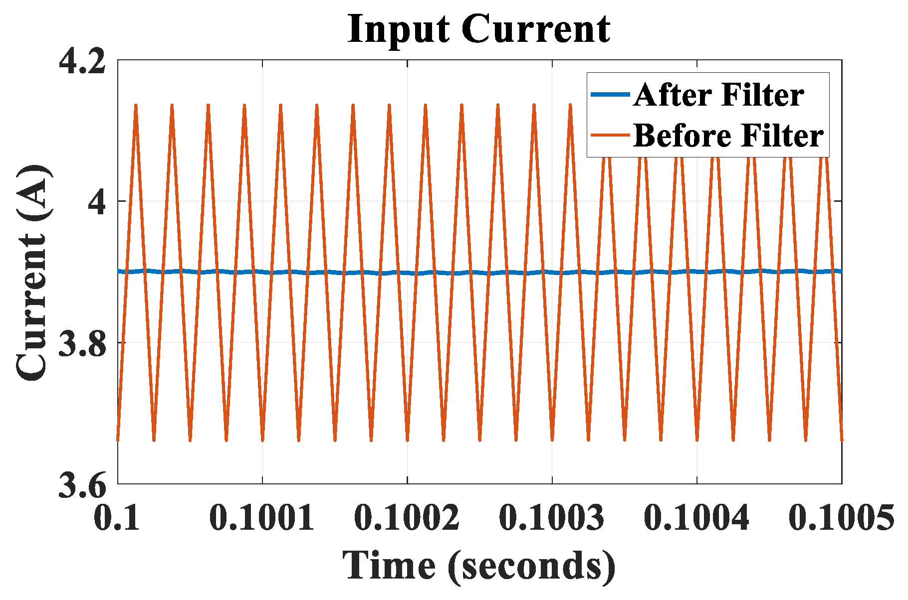
Figure 13 illustrates the current wave form for the input side of the boost converter. As can be seen, the performance of the capacitor as the simple input passive filter was considerable and under the control procedure by the proposed PI controller, a very high quality current wave form could be obtained. This current guarantees a pure DC current for the load.
4. Experimental Results and Discussion
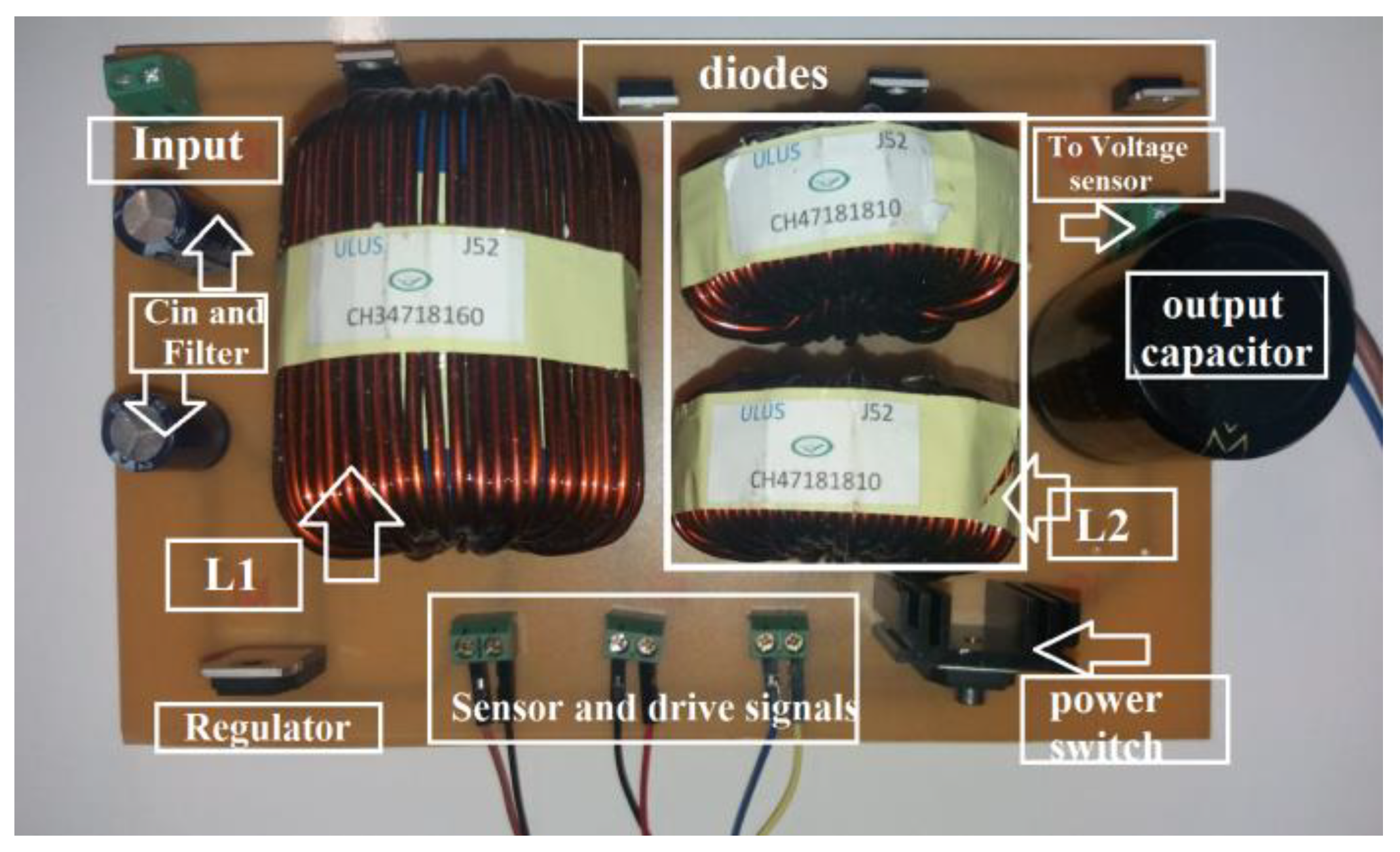
A prototype with around 100 W was implemented and
Figure 14,
Figure 15,
Figure 16 and
Figure 17 show the results. The switching frequency was set to 50 kHz. Inductors
LX and
LY were fixed to 200 uH, the capacitor
C1 value was considered as 1 µF, and the output capacitor C2 as 47 uF.
Figure 14 presents the hardware prototype.
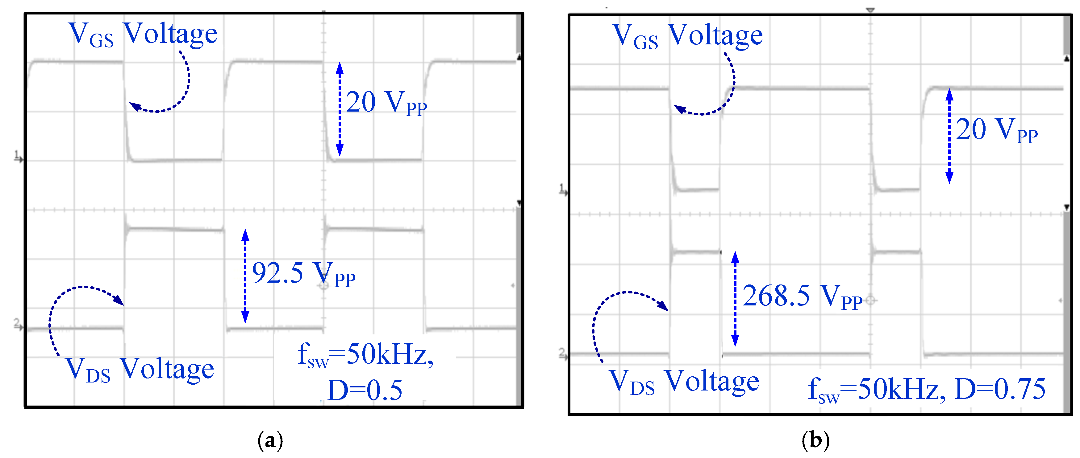
Figure 15 shows the gate source and drain source pulses of the structure in 50% and 75% of duty cycles and as we expected, different values of ON and OFF intervals of power MOSFET and as a result, different duty cycles for the voltages of drain-source pins were obtained.
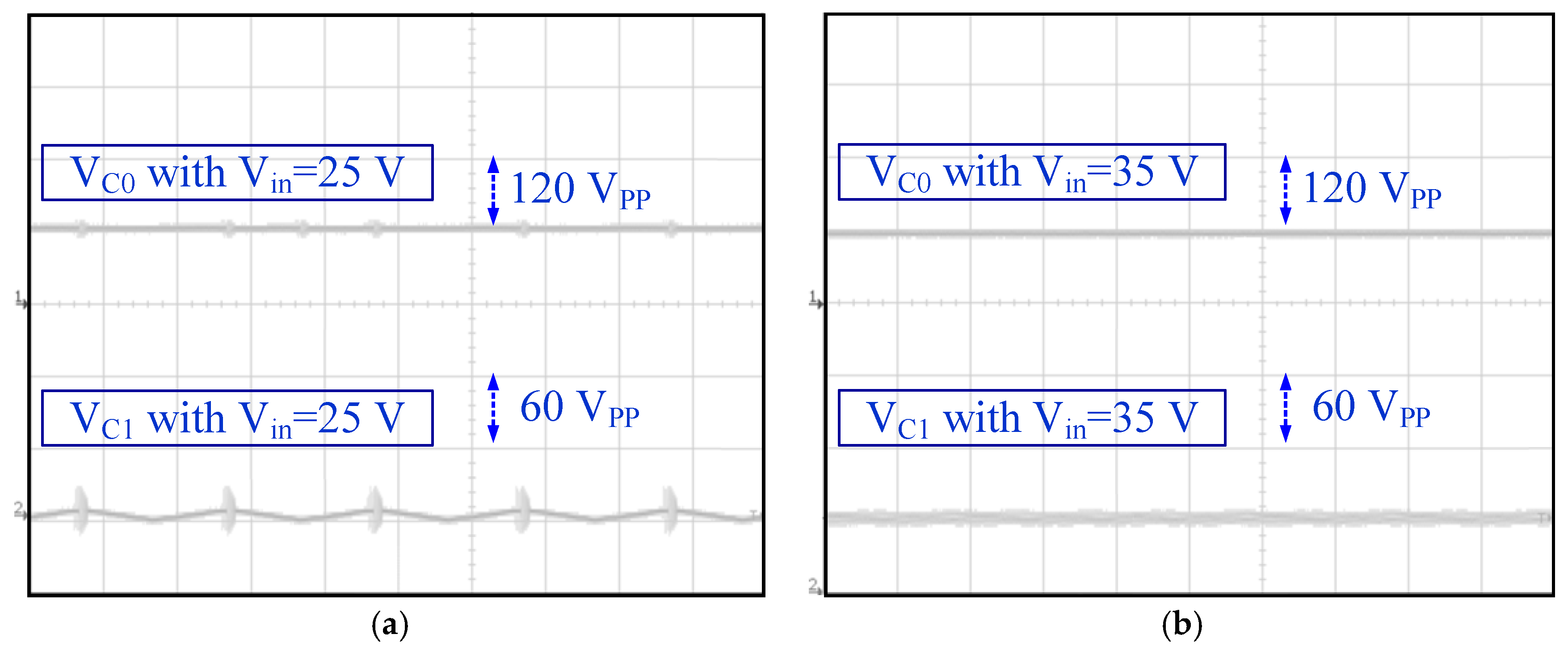
Figure 16 illustrates the voltage waveforms for the capacitors and currents of the inductors.
In
Figure 16a, under 25 V as the input voltage, by applying the proposed controller method, the output voltage was set to 120 V. So, as expected based on Equation (30), half of this value was measured on the first capacitor and the second half of the proposed converter doubled this value on capacitor
C0. This test was undertaken on a 120 Ω resistive load, so the voltages on the capacitors, especially the voltage on capacitor
C1, had fluctuations on switching times. The load value was set to 240 Ω and the input voltage was increased to 35 V for
Figure 16b, and as shown, these sudden ripples decreased. This event is normal because not only was the input voltage increased, but the output current was also a lower level in comparison with the first test.
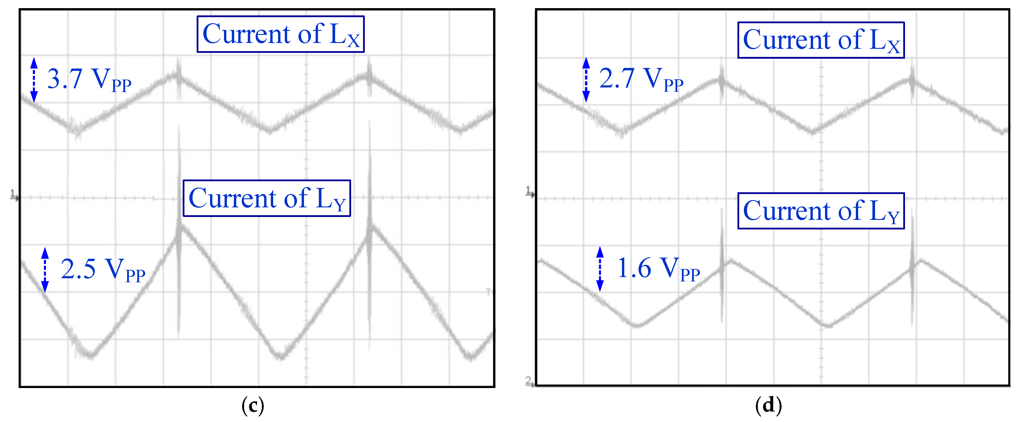
Figure 16c presents the current waveforms of the inductors for a 150 Ω resistive load with 120 V and 25 V as the output and input voltages, respectively. As the results show, the current of the inductor
LY was less and the result confirmed Equations (34) and (35). Additionally, ripple values were reported of around 1.3 and 1.8 A for
LX and
LY, respectively, which is in agreement with the mathematical analysis presented in
Table 1.
Figure 16d reports the results of the same process with a 250 Ω resistive load, 35 V input, and 120 V output voltages. The obtained currents and ripple values confirmed the same equations mentioned for
Figure 16c.
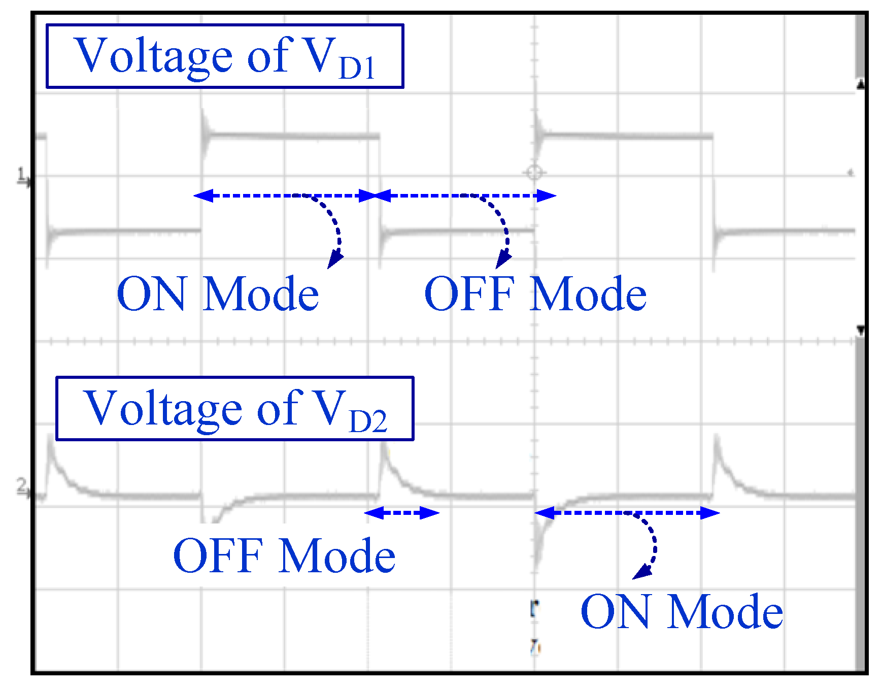
Figure 17 shows the status of the power diodes
D1 and
D2 and confirms the conductivity theory of these diodes in different work principles that was presented in
Section 2.1 in 50% of the duty cycle. Based on this result, when the power diode
D1 is in ON mode,
D2 is in OFF mode and vice versa. A comparison was done in this part between the proposed PI controller and several other controllers in order to assess the performance of the projected structure. Different controllers have been investigated for DC–DC boost converters. The authors in [
23] presented a fault tolerant-based DC–DC boost converter. This structure uses an extra Triode for Alternating Current (TRIAC) and an auxiliary power switch with a DC gain closed to the conventional boost converter. The optimal switching frequency of this converter was adjusted to 20 kHz and the efficiency of the controller was calculated as around 87 percent for low power applications. In [
24], a field-programmable gate array control technique was presented for non-isolated DC–DC converters. The basis of this controller was established on time and the current of the inductor and the robustness of the system was investigated. The controller worked in low switching frequencies around 15 kHz and is suitable for high power applications. The inductor value was comparatively high and at the same time, several internal controller blocks worked to fix the output voltage. The study in [
25] suggested a model-based state estimator approach for the DC–DC converter where the mathematical complexity and specifications of this converter such as switching frequency and inductor value were similar to the method presented in [
24].
A PV-connected DC–DC boost converter using a LUENBERGER observer-based fault detection controller was presented in [
26]. A deep mathematical approach was investigated in this study and the converter block worked as a part of the PV-based maximum power point tracking system. The converter’s disadvantage is not applicable in high switching frequencies and is also proper for high power applications. Therefore, the IGBT is suggested for application instead of the power MOSFET. The authors in [
27] presented a time-domain analysis of the state-space observer residual controller technique for interleaved DC–DC converters. The switching frequency was adjusted to 25 kHz. The total cost of the prototype was categorized in the medium to high range.
Table 4 presents the general specifications of these controllers.
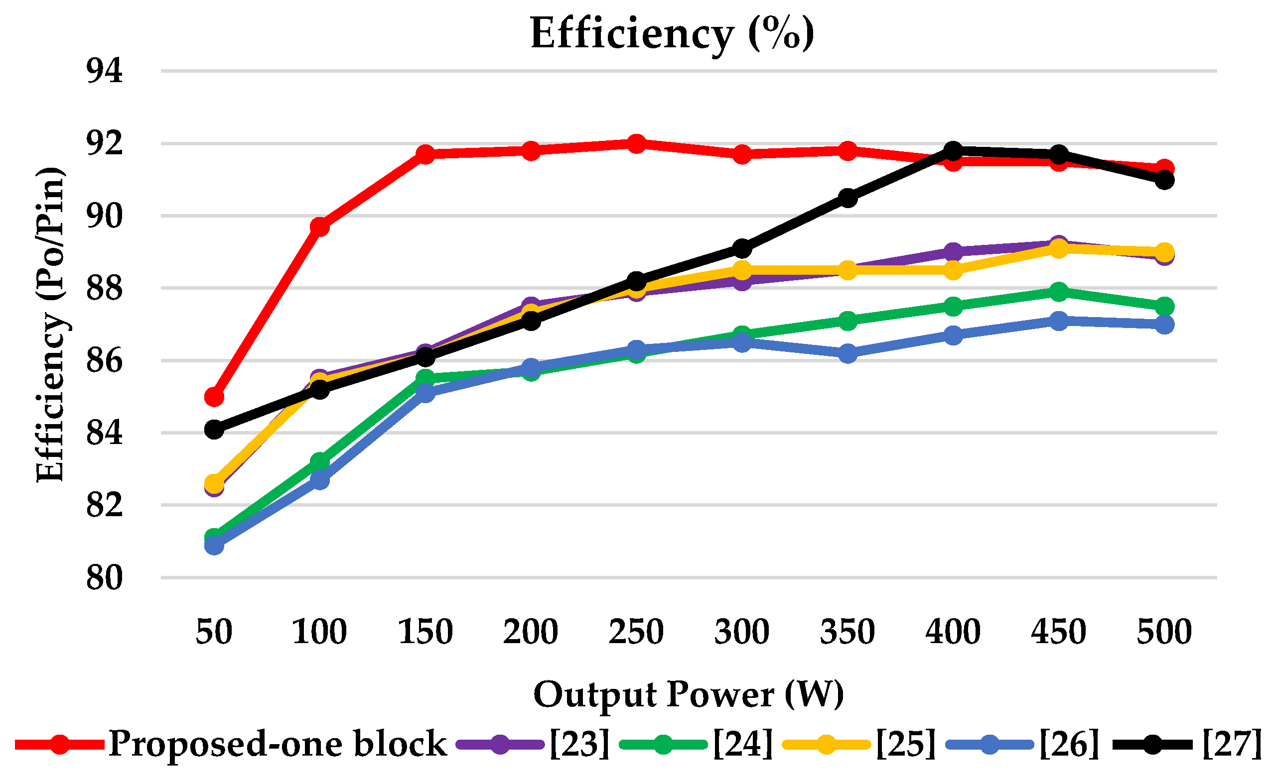
Figure 18 presents the efficiency curves for the presented controllers in
Table 4 versus the output power. As can be seen, the performance of the proposed PI controller is considerable, especially in low powers. It can be interpreted based on all facts presented in
Table 2. Based on less power MOSFET numbers in the converter’s structure and good performance of the proposed PI controller to 350 W, it had the highest efficiency. The performance of the linear observer acts in a similar way to the proposed controller for 350 to 500 power range.
5. Conclusions
This study presents a high gain step-up converter with a simple and cheap controller based on small signal analysis and steady space matrixes. In comparison with the conventional boost converter, the proposed converter uses two additional power diodes, a capacitor, and an inductor. However, the voltage gain of the projected converter is considerable and acts as a cascaded step-up converter. Furthermore, by considering that the topology has only one power switch and in any time interval only two diodes will be in the structure, it presents the same values of the losses in comparison with the cascaded converter by considering the switching, dynamic, and frequency losses. For the controller design, the topology was examined in two ON and OFF states of the switch. So, among all of the equations, the optimal equation that can present a relation between the output voltage and current derivation of the second inductor was selected. The controller was investigated through this equation and the simulation and experimental results showed the robust and stable working conditions for the proposed controller.
A group of simulations was undertaken in MATLAB/SIMULINK 2017a and the results confirmed the theoretical and mathematical analysis. Simulations were done for different values of the input voltages and output loads to generate the different voltages by the PV panels based on the irradiance and temperature. Therefore, a good controller should present stable and fixed DC voltages for the different values of this input source. Additionally, the stability of the structure and controller is important when different values of loads are entered at the output side of the structure. The results showed that for 24 V and 50 Ω as the output load, the controller can reach the fixed desired 120 V with around 0.12 S, which is acceptable for a topology that will work for a long time. A laboratory scaled prototype was implemented. For a 24 V input source, since the simulation results give 93 V as the output voltage in 50% of duty cycles, the prototype can present around 92.5 V, which is acceptable and confirms the theoretical analysis and simulation results. Working in lower switching frequencies will help to decrease the voltage and current stresses on power switches where a high gain application is necessary. As a suggestion, soft switching and snubber sub-structures can be utilized to decrease these stresses.

 ,
, 


