Article

Resistivity and Its Anisotropy Characterization of 3D-Printed Acrylonitrile Butadiene Styrene Copolymer (ABS)/Carbon Black (CB) Composites

Faculty of Biomedical Engineering, Fourth Military Medical University, 169 West Changle Road, Xi’an 710032, China
*
Authors to whom correspondence should be addressed.
These authors contributed equally to this work.
Appl. Sci. 2017, 7(1), 20; https://doi.org/10.3390/app7010020
Submission received: 17 October 2016 / Revised: 14 December 2016 / Accepted: 19 December 2016 / Published: 4 January 2017
(This article belongs to the Section Materials Science and Engineering)

Abstract

:
The rapid printing of 3D parts with desired electrical properties enables numerous applications. Fused deposition modeling (FDM) using conductive thermoplastic composites has been a valuable approach for such fabrication. The parts produced by FDM possess various controllable structural features, but the effects of the structural features on the electrical properties remain to be determined. This study investigated the effects of these features on the electrical resistivity and resistivity anisotropy of 3D-printed ABS/CB composites. The effects of the process parameters of FDM, including the layer thickness, raster width, and air gap, on the resistivity in both the vertical and horizontal directions for cubic samples were studied because the internal structure of the printed parts depended on those process parameters. The resistivities of printed parts in different parameter combinations were measured by an impedance analyzer and finite element models were created to investigate the relationship between the resistivity and the internal structure. The results indicated that the parameters remarkably affected the resistivity due to the influence of voids and the bonding condition between adjacent fibers. The resistivity in the vertical direction ranged from 70.40 ± 2.88 Ω·m to 180.33 ± 8.21 Ω·m, and the resistivity in the horizontal direction ranged from 41.91 ± 2.29 Ω·m to 58.35 ± 0.61 Ω·m at the frequency of 1 kHz. Moreover, by adjusting the resistivities in different directions, the resistivity anisotropy of the printed parts can be manipulated from 1.01 to 3.59. This research may serve as a reference to fabricate parts with sophisticated geometry with desired electrical resistivity and resistivity anisotropy.

1. Introduction

3D printing, also known as additive manufacturing, enables the construction of parts with complex geometries without the need for expensive molds or tools. As such, the method is potentially profitable for both scientific research [1] and commercial manufacturing [2]. With its rapid development in recent years, 3D printing has evolved from manufacturing prototypes to building functional components in numerous fields, ranging from mechanical engineering [3] and biomedical engineering [4,5,6], to electrochemical studies [7]. For applications in various fields, developing and characterizing printable materials with desired properties are currently key areas of research and development.
Materials with desirable electrical properties are indispensable for many research and industrial areas. Materials of controlled electrical resistivity can be employed for controlled electrical conduction, static charge dissipation, and lightning protection in electronics [8].Those materials often require processing before being employed and 3D printing, a useful processing method for fabrication of complex shape parts, has been used to print objects with desired electrical properties. There are currently two main approaches. In one approach, the objects are fabricated to a required geometry using insulating materials, and then conductive additives are embedded in the objects to obtain electrical conductivity [9,10,11].In the other approach, the objects are directly printed with conductive materials [12,13,14,15,16,17]. The second approach is more efficient, and its application areas include electronic sensors [18,19], paper electronics [20], light-emitting diodes [21], microbatteries [22],and electrodes [23,24].The conductive materials for 3D printing mainly comprise metal, carbon, and their polymer composites. The feedstock of polymer composites mixed with various forms of carbon has attracted considerable attention because carbon cannot be oxidized and then become nonconductive. In addition, the polymer composites are always thermoplastic and, thus, can be handled by fused deposition modeling (FDM), a widely used 3Dprinting technology. For instance, Leigh et al. reported a method to fabricate electronic sensors using low-cost 3D FDM printing by polycaprolactone (PCL)/carbon black (CB) [18]. Although the materials appeared to have low resistivity after printing, they did not evaluate the influence of the process of FDM on the resistivity of printed parts. Wei et al. revealed that the resistivity of printed parts was much higher than that of the feedstock for acrylonitrile butadiene styrene copolymer (ABS)/graphene oxide (GO) composites [15]. However, the reason why the resistivity was increased was not described in detail. To the best of our knowledge, despite the potential of these materials for various applications, few studies have specifically characterized the resistivity of 3D-printed conductive composites.
Although the resistivity of the composites is mainly determined by the conductive additives, the process technique and the process parameters are also important factors that influence resistivity [25]. For example, in the traditional injection molding, the process parameters significantly influence the electrical conductivity of molded composites [26]. Additionally, in 3D printing, FDM produces 3D objects by extruding thermoplastic materials and depositing the semi-molten materials onto a stage layer by layer. Microscopically, voids inevitability exist within the model, and adjacent fibers may not be completely fused because the material is semi-molten when deposited [27]. The process parameters considerably influence the mechanical properties [28,29,30,31] and the dimensional accuracy [32] of the printed parts. As the resistivity of the materials are also influenced by the inner microstructure, we hypothesize that the structural features affected by the process parameters also affect the resistivity of the printed parts.
Another obvious characteristic of printed parts is structural anisotropy [33], namely the structures in horizontal direction and vertical direction of printed parts inherently are different. Structural anisotropy of the printed parts of conductive composites also produces anisotropy in resistivity [18]. Especially, considering their stacked structure, printed parts provide a complete conductive path in the horizontal printing direction of the fibers. However, perpendicular to such direction, the formation of a conductive pathway is reliant on the melting between adjacent printed fiber layers [18], which is affected by the process parameters. Since the process parameters affect the internal fiber structure of the printed parts, we hypothesize that the parameters also influence the resistivity anisotropy and the relationship between the anisotropy ratio and the process parameters must be clarified to fabricate parts with controllable resistivity anisotropy.
Accordingly, this study aims to characterize the resistivity and its anisotropy of 3D-printed parts derived from ABS/CB composites. As it is proven that the resistivity of printed parts is much higher than that of the feedstock, we herein attempt to investigate how the parameters influence the internal structure and, hence, affect the resistivity and its anisotropy of 3D-printed ABS/CB parts. Based on these findings, we present a new method to fabricate 3D components of controllable resistivity and its anisotropy.

2. Materials and Methods

2.1. The Fabrication of Filaments and Printed Parts

ABS is a standard material used in 3D printers for fused deposition, and CB is a suitable filler material in conductive polymer composites. As such, ABS/CB composite pellets with 15 wt% CB, a composite with good conductive performance [34], was chosen. ABS/CB conductive composite pellets (Guangzhou Plastic Technology Co., Ltd., Guangzhou, China) were extruded into a 1.75 mm diameter filament to fit the 3D printer using a single screw extruder [35] (Supplementary Materials, Figure S1). Due to the swell phenomenon during extrusion, a discrepancy in diameter exists between the nozzle and the produced filament. A copper nozzle with an internal diameter of 1.70 mm was chosen to produce a filament with an average diameter of 1.75 mm and a standard deviation of 0.03 mm.
An open source 3D printer, Prusa i3, was used to fabricate the samples (Figure S2). The dimensions of the cubic sample are 20 mm × 20 mm × 20 mm (length × width × height). Afterwards, a series of experiments was carried out using a three-level, three-factor factorial design to study the influence of three process parameters, i.e., layer thickness (A), raster width (B), and air gap (C), on the resistivity and its anisotropy. The typical parameter value was selected as the middle level, and the two other levels were chosen on the basis of the literature [28] as shown in Table 1. Each parameter was controlled independently through the slice software (Slic3r, Version 1.0), referring to the parameter combinations of the array in Table S1. Such experimental design could obtain all possible parameter combinations. The other fixed process parameters were as follows: nozzle diameter (0.4 mm), movement speed of the nozzle during printing (100 mm/s), extrusion temperature (230 °C), hot bed temperature (110 °C), and extrusion speed (generated automatically by the slice software depending on the nozzle movement speed and material diameter). Moreover, two parameters were set for all of the samples to ensure surface smoothness, thus facilitating resistance measurement. To improve the precision and to estimate the standard deviation, three samples for each parameter combination were produced.

2.2. Resistivity Measurement

Sample resistivity was measured using an impedance analyzer (Solartron SI1260, Schlumberger, New York, NY, USA) with a general-purpose interface board (GPIB) and a computer for system control and data input/output (Figure S3). Silver-plated copper conductive rubber (Shenzhen Brilliance Rubber and Plastic Materials Co., Ltd., Shenzhen, China) with a resistivity less than 10−4 Ω·m was used as the measuring electrode. By virtue of the elasticity of the conductive rubber, excellent contact between the electrode and the sample surface was attained to reduce the contact resistivity between the sample and electrode. The test cell with the conductive rubber electrode can be seen in Figure S3b. We evaluated the contact resistivity by measuring samples with the same cross-sectional area and different heights in the test cell and it revealed that the contact resistivity was negligible compared with the resistivity of the samples.
Filament and fiber resistivities were measured using the two-electrode method, and the cubic sample resistivity was measured by the four-electrode method. Both of the measurements were conducted with a 0.5 mA drive current in sweep frequency mode in the frequency range of 1 Hz–1 MHz. For the cubic sample, the measurement was carried out in the vertical and two horizontal directions, and the mean value of the measurements in the two horizontal directions was used as the final resistivity in the horizontal direction. The vertical direction refers to the object’s building direction, namely, the growth direction during object generation. The horizontal direction includes two directions, namely, the width and length directions, and the resistivities in the two directions are identical in theory (the difference of them is less than 2% in actual measurement). The resistivity anisotropy was defined as the ratio of resistivity in the vertical direction to resistivity in the horizontal direction. The resistivity of each sample was measured thrice, and the average was obtained to decrease measuring error. In addition, conductive composites are affected by temperature; hence, measurements were performed at isoperibol (25 ± 0.3 °C) in a controlled temperature box as shown in Figure S3a.

2.3. Data Processing, Simulation,and Scanning Electron Microscopy

The data measured from different parameter combinations were analyzed using statistical software (Minitab 16, Minitab Inc, State College, PA, USA).The main effects were used to evaluate the influence of each parameter on the resistivities. Moreover, as the parameters influence the resistivity via changes in the internal structure, simulation of the relationship between the resistivity and the internal structure of 3D-printed parts was carried out using the finite element simulation software (COMSOL Multiphysics 5.2, COMSOL Inc, Stockholm, Sweden). In the simulation models, the resistivity of the fibers was the same as that of the filament. To calculate the resistivity of the models, two copper electrodes of 0.5 mm thickness were added to two sides of the simulation models. One electrode was driven by 1 A/m2 current density, and the other electrode was grounded. Finally, scanning electron microscopy (S-3400N, Hitachi, Tokyo, Japan) was used to characterize the internal structure of the printed parts.

3. Results and Discussion

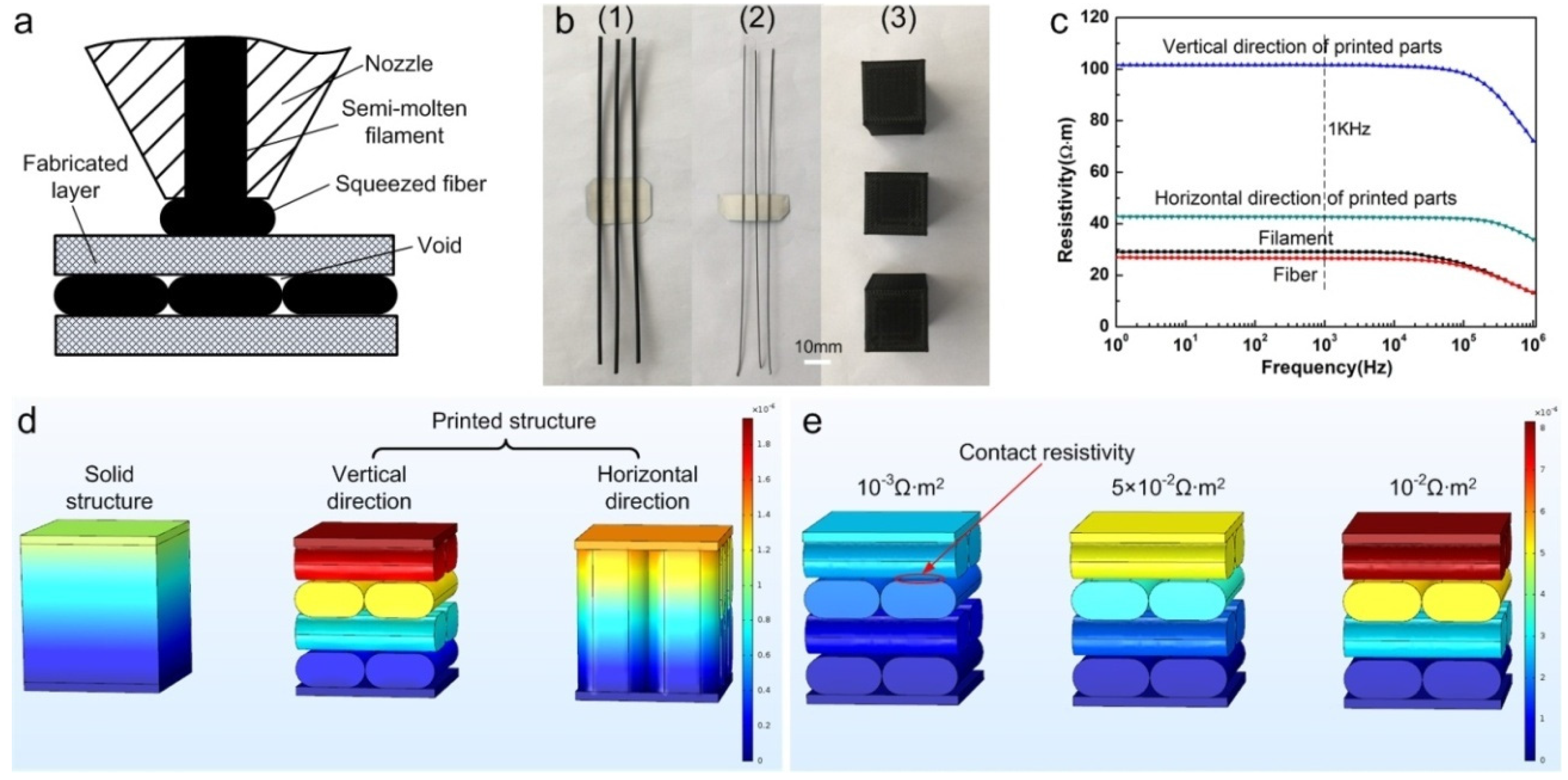
3.1. Resistivities of Filaments and Printed Parts

In FDM, the filaments were heated into a semi-molten state and extruded into thin fibers from a nozzle of the 3D printer. The fibers were deposited layer by layer according to the sliced model design to build 3D models (Figure 1a). To compare the resistivity of the ABS/CB composites in different shapes, the resistivities of the filaments, fibers, and the cubic samples (Figure 1b) at frequencies of 1Hz–1 MHz were measured and are shown in Figure 1c, wherein cubic samples were fabricated by a default process parameter combination (layer thickness: 0.2 mm, raster width: 0.4 mm, air gap: 0.00 mm). The resistivities of differently-shaped parts were relatively constant from 1 Hz to 100 kHz, and then decreased gradually from 100 kHz to 1 MHz.The resistivities of the cubic samples are much higher than those of the filaments, as reported previously for ABS/GO composites [15], and the resistivities of the extruded fibers wereslightly lower than those of the filaments. In addition, the resistivities of the cubic samples significantly varied in different directions (Figure 1c), which is consistent with previous reports [18]. For instance, at a frequency of 1 kHz, the resistivities of the filaments, the fibers, the samples in the horizontal direction and the samples in the vertical direction were 29.06 ± 0.77 Ω·m, 26.55 ± 0.50 Ω·m, 42.59 ±1.94 Ω·m and 101.60 ± 6.85 Ω·m, respectively. It can,thus,be concluded that the resistivities of the cubic samples increased compared to the fibers, but the resistivities of the filaments did not increase compared to the fibers. Consequently, the possible reason was due to the internal structural features of the printed parts produced during deposition of the fibers but not to the heating and extruding process of the materials.
To investigate why the resistivity changed from fibers to the printed samples, a finite element model was established to simulate the printed structure that was created from the fibers. The cross-section of the fiber is circular when the material extrudes from the nozzle, but the fiber becomes squeezed and deformed when deposited. The fiber was modeled with two straight sides and two rounded sides [28], as shown in Figure 1a. The advantage of this model was that the mass density decrease from the solid model to the printed structure model was similar to the actual case considering the existence of voids for printed parts. Specifically, the density decreased from 1.178 g/cm3 for the ABS/CB composite filament to 1.051 g/cm3 for the printed parts and the density ratio of the printed structure to solid structure was 0.891 for simulation models. The simulation results indicated that the resistivities of the printed structure in the vertical and horizontal directions are 1.85 and 1.38 times of those of the cubic solid model, respectively, as shown in Figure 1d. In fact, the measured values were 3.83 and 1.60 times. Therefore, voids may not be only factor to determine the resistivities of cubic samples. Although using a greater void fraction in the simulation model could increase the predicted resistivity, it also unavoidably decreases the density further, inconsistent with the actual case.
The fibers extruded from the nozzle are semi-molten [27,28,36] and not completely fused. The imperfect bonding conditions between adjacent fibers may cause contact resistivity. Hence, besides voids, the influence of this contact resistivity between fiber layers on the resistivity in the vertical direction was also examined in the simulation model. As shown in Figure 1e, the resistivity indicated by the model increased with contact resistivity. The relationship between the resistivity in the vertical direction and the contact resistivity was given in Figure S4. When the contact resistivity was 3.16 × 10⁻³ Ω·m2, the resistivity of the deposited structure in the vertical direction was approximately3.83 times that of the solid structure, which was identical to the measured value. In addition, it can be seen in Figure 1d,e that, regardless of the presence of the contact resistivity, the resistance of the whole sample mainly emerges between the fibers rather than within the fibers. It suggests that the interlayer bonding, including the bonding area and the bonding quality, may significantly influence the resistivity in the vertical direction of the printed parts.

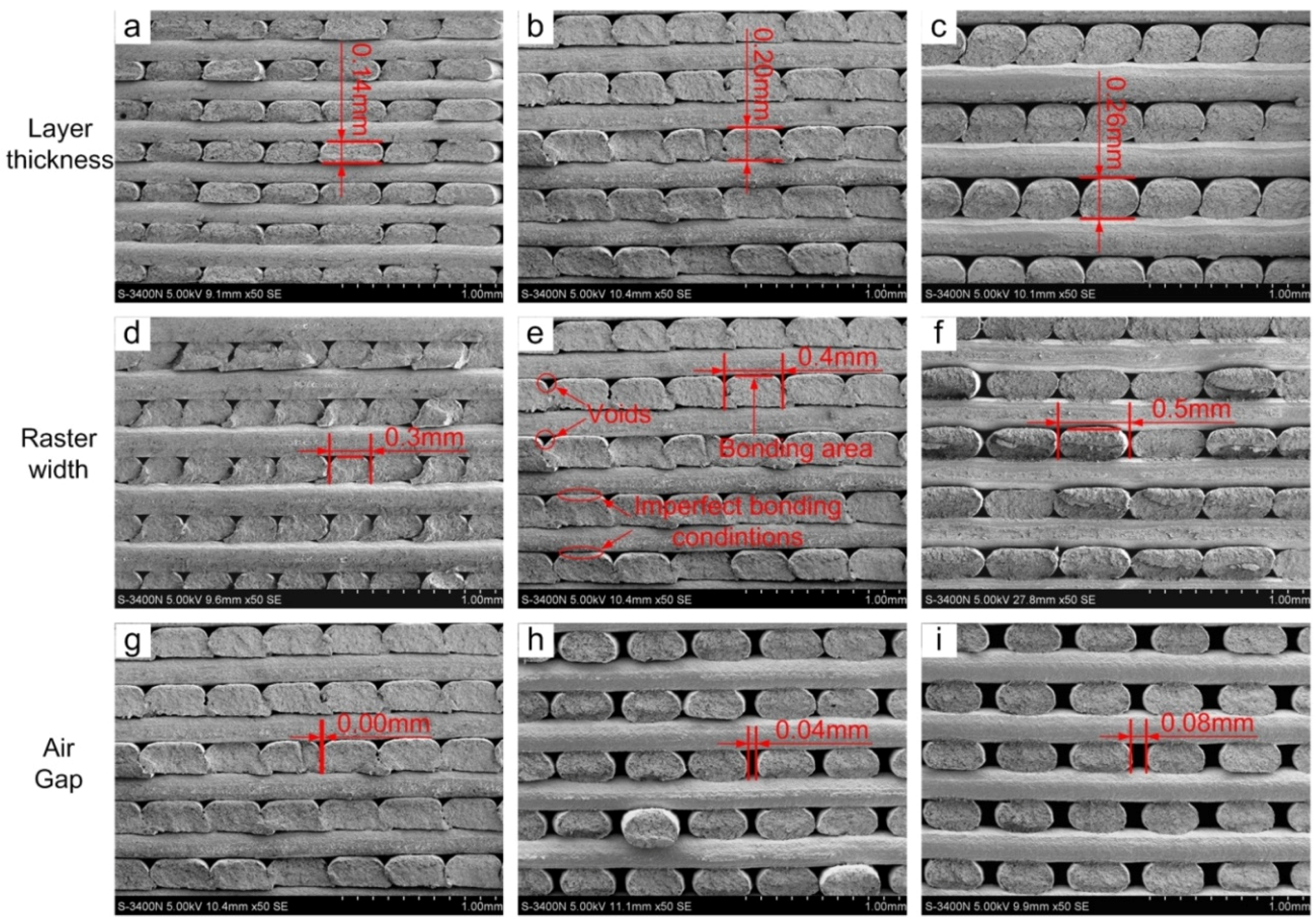
3.2. Influence of Process Parameters on the Resistivities of Printed Parts

The influence of three process parameters, i.e., layer thickness, raster width, and air gap (as shown in Figure 2a), was investigated by a three-level, three-factor factorial design. The resistivities of the samples (frequency = 1 kHz) in the vertical and horizontal directions were measured and shown in Figure 2b. The resistivity was higher in the vertical direction than in the horizontal direction for all of the samples. Compared with the resistivity in the horizontal direction, the resistivity in the vertical direction was more readily affected by the process parameters. Specifically, the maximum resistivity in the vertical direction was more than two times greater than that of the minimum value.
Data on the resistivity in the vertical direction were further analyzed using statistical software to determine the importance of each factor. Figure 2c shows the effect of each independent variable (AC) on the resistivity in the vertical direction of the samples, namely average values and standard deviations. Among the three parameters, the effect of B (raster width) was much greater than those of A (layer thickness) and C (air gap). With increasing raster width, the resistivity in the vertical direction decreased significantly. With increasing the air gap, the resistivity increased slightly, and the effect of the layer thickness on the resistivity in the vertical direction was not obvious. Moreover, the optimum A, B, and C showing the lowest electrical resistivity in the vertical direction was A1B3C1 (layer thickness: 0.14 mm, raster width: 0.5 mm, air gap: 0.00 mm).
The effect of the main factors derived from the statistical analysis on the resistivity in the horizontal direction is presented in Figure 2d. A (layer thickness) exerted the greatest effect on the resistivity of the samples, with the resistivity in the horizontal direction increasing with layer thickness. C (air gap) also evidently influenced the resistivity, with the resistivity in the horizontal direction increasing with the air gap. In addition, the effect of B (raster width) on resistivity in the horizontal direction was not significant, and the optimum A, B, and C showing the lowest electrical resistivity in the horizontal direction was A1B2C1 (layer thickness: 0.14 mm, raster width: 0.4 mm, air gap: 0.00 mm).
To further explain these findings, we conducted simulation experiments to clarify the relationship between the resistivity and internal structure for simulated parts similar to the printed ones. The influence of raster width and air gap on the resistivity in the vertical direction and layer thickness and air gap on the resistivity in the horizontal direction was examined as the effect of layer thickness on the resistivity in the vertical direction and raster width on the resistivity in the horizontal direction was not obvious. The result of the simulation examining the influence of the raster width on the resistivity in the vertical direction is shown in Figure 3a. As the resistivity of the fibers remained the same in the models with different raster widths, the differences between these models were the structure. For different raster widths, the void area was the same between parallel fibers, and the difference was the bonding area between fiber layers. It appears that with increasing raster width, the bonding area increased, and this decreased the resistivity in the vertical direction. In addition, the air gap also had a significant impact on the resistivity. It is obvious that, with the increasing air gap, the void area was enlarged and this increased the resistivity in the vertical direction. Comparing Figure 3a,b, it is shown that the influence of raster width was more significant than that of the air gap, maybe indicating the effect of the contact condition was greater than voids in the vertical direction.
The simulation results for the influence of the layer thickness and the air gap on the resistivity in the horizontal direction are shown in Figure 3c,d. We can see that increasing the layer thickness and air gap enlarged the void area. As the current was passed along the fiber in the horizontal direction, the bonding condition between adjacent fibers did not significantly affect the resistivity. It appears that the voids were the main reason that impacts resistivity in the horizontal direction.
For the further investigation of the relationship between the resistivity of 3D-printed parts and their structural properties affected by the process parameters, scanning electron microscopy (SEM) was used to analyze the structural features of the printed parts as shown in Figure 4. We observed from the SEM images that the shape of deposited fibers from different process parameters was similar to that employed in the simulation models, namely, fibers with across-sectional area bound by two straight parallel sides and two rounded sides. Specifically, for images of different layer thicknesses, the void area increased and the number of layers decreased with the increase of layer thickness as indicated in Figure 4a–c. For images of different raster widths, it can be observed that the shape and area of the voids resulting from different raster widths was almost the same and that the bonding area increased with increasing raster width as shown in Figure 4d–f, and both of these observations were the same as the simulation model predictions. For images of different air gaps, the voids significantly increased with the air gap as given in Figure 4a–c, which must induce the increase of resistivities in two directions.
A feature of the actual internal structure of printed parts that was different with the simulated structure was that the actual bonding condition was not perfect between adjacent fibers, as shown in Figure 4. The imperfect bonding condition must induce the arising of the contact resistivity between adjacent fibers and increase the resistivity of the printed parts, especially in the vertical direction. In the simulation analysis, when a contact resistivity existed, the decrease of the resistivity in the vertical direction was more substantial with the increasing raster width, as shown in Figure S4c, which can explain the resistivity decrease from 154.87 Ω·m to 89.07 Ω·m when the raster width changed from 0.3 mm to 0.5 mm.
For the structure of printed parts, current in the vertical direction must pass through the adjacent fiber layers to obtain electrical conductivity. For the simulation analysis, the increase of the resistivity in the vertical direction occurs between the fiber layers, and the presence of the contact resistivity between the fiber layers increases the resistivity of the whole structure. In addition, with the increase of the raster width, the contact area between the fibers increased, and the resistivity decreased. Hence, the evidence of simulation and electron microscopy analysis could demonstrate bonding conditions, including the bonding area and bonding quality, which are the most important factors that affect the resistivity in the vertical direction. On the other hand, the current in the horizontal direction cannot only spread along the fiber, but also transmit through the adjacent parallel fibers from the structure of printed parts. The presence of voids reduces the contact of the adjacent fibers, as well as the effective cross-sectional area of the fibers and, therefore, may increase the resistivity. Both simulation and electron microscopy proved the results. Thus, voids are supposed to be the most important factor to affect resistivity in horizontal direction.
The electrical conductivity of ABS/CB is afforded by the conductive fillers and the structure of contact between carbon filler is a factor to affect the resistivity of printed parts, but the main issue we focused on were structural features within the scope of extruded fibers, and the influence of contact between carbon filler on resistivity could be found in other studies [37,38]. In addition, although the shape of the actual fibers and the bonding condition between adjacent fibers had some inconsistencies, which may be caused by inaccuracies in the positioning stage or the extrusion rates, the effect of these deviations on resistivity was slight because the fibers are relatively small in size and the error due to each fiber was averaged over a number of fibers. Therefore, there is evidence that the resistivity in the vertical direction can be adjusted by changing the raster width.

3.3. Control of the Resistivity Anisotropy of Printed Parts

The internal structure of the printed parts inherently appears anisotropic, and when the printed parts serve as a conductive medium, the resistivity is also anisotropic [18]. In the vertical direction, the current must pass through adjacent fiber layers but, in the horizontal directions, the current is not distributed only along the individual fiber but also across parallel fibers. As the process parameters influence the structure of printed parts, it also impacts the resistivity anisotropy ratios of the parts. The resistivity anisotropy ratios for the different parameter combinations are shown in Figure 5a by calculating the ratio of the resistivity in the vertical direction to that in the horizontal direction. The maximum anisotropy ratio is 3.59 and the minimum ratio is 1.47. The effect of the main factors of the anisotropy ratio for the three parameters is indicated in Figure 5b. Similar to that of resistivity in the vertical direction, the most influential parameter was the raster width, and the anisotropy ratio decreased with increasing raster width.
To further clarify the relationship between the anisotropy ratio and raster width, the anisotropy ratio for the raster width range of 0.30 to 0.70 mm at intervals of 0.05 mm was examined. It can be seen from Figure 5c that with increasing raster width, the resistivity anisotropy ratio decreased monotonically. Although the structure of the printed parts was anisotropic when the raster width was 0.70 mm, the resistivity anisotropy ratio was close to 1.0. This result suggested that the resistivity of the printed parts can be adjusted to be nearly isotropic. This indicated that although the internal structure of printed parts was inevitably anisotropic, isotropic resistivity for conductive composites can be achieved by adjusting the process parameters. The relationship between the anisotropy ratio and raster width was fitted by an exponential function as shown in Figure 5c. The correlation coefficient was 0.993. It can be concluded that the resistivity anisotropy ratio can be adjusted from 1.01 to 3.59 by directly altering the raster width. Therefore, this could be considered as a new approach to fabricate parts with complex shapes and desired resistivity anisotropy ratio. Further, although the resistivity anisotropy ratio manipulation can also be achieved by printing with two kinds of materials with different resistivities using a two-nozzle printer, the advantage of this method was that only one conductive composites and the most widely used one-nozzle printer were needed.
Since controllable and well-defined anisotropy materials are required in the construction of phantoms to test methods that evaluate medical imaging equipment, such as diffusion tensor imaging [39] and electrical impedance tomography [40], the process we detailed to manipulate resistivity anisotropy may serve as a new approach to fabricate a model by 3D printing with a complex shape and the desired resistivity anisotropy for imaging electrical anisotropy.

4. Conclusions

The aim of this study was to investigate resistivity and its anisotropy characterization of 3D-printed conductive composites. A conductive, CB-filled ABS filament for a fused filament modeling printer was created. Comparing the resistivity of the filaments and cubic samples made by 3D-printing, it can be concluded that the resistivity of the printed samples increased remarkably. Specifically, the resistivity increased from 29.06 Ω·m ± 0.77 Ω·m for the filaments to 42.59 ± 1.94 Ω·m and 101.60 ± 6.85 Ω·m for the cubic samples in the horizontal direction and the vertical direction, respectively.
The influence of process parameters, i.e., layer thickness, raster width, and air gap, on the resistivity of the 3D-printed parts was also studied. Raster width and air gap significantly affected the resistivity in the vertical direction, and layer thickness and air gap significantly affected the resistivity in the horizontal direction. It was evident that process parameters affected the internal structure of printed parts and influenced the resistivity. It also appeared that a wider raster width produced a greater bonding area, which decreased the resistivity in the vertical direction; a greater air gap produced a larger void, which increased the resistivity; increasing either the layer thickness or the air gap produced larger voids and then increased the resistivity in the horizontal direction. Hence, the resistivity of printed parts can be adjusted by carefully changing the process parameters.
The resistivity of the printed parts was anisotropic as the internal structure of the parts was anisotropic. The process parameters alter the internal structure and, thus, modify the resistivity anisotropy ratio simultaneously. This study indicates that the resistivity anisotropy ratio can be adjusted from 1.01 to 3.59 by adjusting the raster width. This feature offers an efficient and reliable method to fabricate objects with controllable resistivity anisotropy.

Supplementary Materials

The following are available online at www.mdpi.com/2076-3417/7/1/20/s1. Figure S1: The fabrication of filaments from pellets by the single screw extruder, Figure S2: The fabrication of samples by 3D printer, Figure S3: Resistivity measurement system, Figure S4: The relationship between the resistivity in the vertical direction and the contact resistivity, Table S1: Experimental design showing the three-level, three-factor factorial design and experimental results.

Acknowledgments

This work was supported by the National Natural Science Foundation of China under Grant 51477176 and 31600799.

Author Contributions

J.Z. and X.D. conceived and designed the experiments. J.Z., B.Y., M.D., F.F., and F.Y. carried out the experiments. J.Z., B.Y., M.D., F.F., and F.Y. analyzed the data. J.Z. and B.Y. wrote the paper. All authors reviewed the manuscript.

Conflicts of Interest

The authors declare no conflict of interest.

References

  1. Pearce, J.M. Building research equipment with free, open-source hardware. Science 2012, 337, 1303–1304. [Google Scholar] [CrossRef] [PubMed]
  2. Bogue, R. 3D printing: The dawn of a new era in manufacturing? Assem. Autom. 2014, 33, 307–311. [Google Scholar] [CrossRef]
  3. Tekinalp, H.L.; Kunc, V.; Velez-Garcia, G.M.; Duty, C.E.; Love, L.J.; Naskar, A.K.; Blue, C.A.; Ozcan, S. Highly oriented carbon fiber-polymer composites via additive manufacturing. Compos. Sci. Technol. 2014, 105, 144–150. [Google Scholar] [CrossRef]
  4. Wang, X.; Ao, Q.; Tian, X.; Fan, J.; Wei, Y.; Hou, W.; Tong, H.; Bai, S. 3D bioprinting technologies for hard tissue and organ engineering. Materials 2016, 9, 802. [Google Scholar] [CrossRef]
  5. Jakus, A.E.; Secor, E.B.; Rutz, A.L.; Jordan, S.W.; Hersam, M.C.; Shah, R.N. Three-dimensional printing of high-content graphene scaffolds for electronic and biomedical applications. ACS Nano 2015, 9, 4636–4648. [Google Scholar] [CrossRef] [PubMed]
  6. Wang, D.; Wang, Y.; Wang, J.; Song, C.; Yang, Y.; Zhang, Z.; Lin, H.; Zhen, Y.; Liao, S. Design and fabrication of a precision template for spine surgery using selective laser melting (SLM). Materials 2016, 9, 608. [Google Scholar] [CrossRef]
  7. Ambrosi, A.; Pumera, M. 3D-printing technologies for electrochemical applications. Chem. Soc. Rev. 2016, 45, 2740–2755. [Google Scholar] [CrossRef] [PubMed]
  8. Chung, D. Electrical applications of carbon materials. J. Mater. Sci. 2004, 39, 2645–2661. [Google Scholar] [CrossRef]
  9. Salvo, P.; Raedt, R.; Carrette, E.; Schaubroeck, D.; Vanfleteren, J.; Cardon, L. A 3D printed dry electrode for ecg/eeg recording. Sens. Actuators APhys. 2012, 174, 96–102. [Google Scholar] [CrossRef]
  10. Swensen, J.P.; Odhner, L.U.; Araki, B.; Dollar, A.M. Printing three-dimensional electrical traces in additive manufactured parts for injection of low melting temperature metals. J. Mech. Robot. 2015, 7, 021004. [Google Scholar] [CrossRef]
  11. Cooperstein, I.; Layani, M.; Magdassi, S. 3D printing of porous structures by uv-curable o/w emulsion for fabrication of conductive objects. J. Mater. Chem. C 2015, 3, 2040–2044. [Google Scholar] [CrossRef]
  12. Postiglione, G.; Natale, G.; Griffini, G.; Levi, M.; Turri, S. Conductive 3D microstructures by direct 3D printing of polymer/carbon nanotube nanocomposites via liquid deposition modeling. Compos. Part A Appl. Sci. Manuf. 2015, 76, 110–114. [Google Scholar] [CrossRef]
  13. Zhang, Q.; Zhang, F.; Medarametla, S.P.; Li, H.; Zhou, C.; Lin, D. 3D printing of graphene aerogels. Small 2016, 12, 1702–1708. [Google Scholar] [CrossRef] [PubMed]
  14. Layani, M.; Cooperstein, I.; Magdassi, S. Uvcrosslinkable emulsions with silver nanoparticles for inkjet printing of conductive 3d structures. J. Mater. Chem. C 2013, 1, 3244–3249. [Google Scholar] [CrossRef]
  15. Wei, X.; Li, D.; Jiang, W.; Gu, Z.; Wang, X.; Zhang, Z.; Sun, Z. 3D printable graphene composite. Sci. Rep. 2015, 5. [Google Scholar] [CrossRef] [PubMed]
  16. Roberson, D.A.; Wicker, R.B.; Murr, L.E.; Church, K.; MacDonald, E. Microstructural and process characterization of conductive traces printed from ag particulate inks. Materials 2011, 4, 963. [Google Scholar] [CrossRef]
  17. Ambrosi, A.; Moo, J.G.S.; Pumera, M. 3D printing: Helical 3D-printed metal electrodes as custom-shaped 3d platform for electrochemical devices. Adv. Funct. Mater. 2016, 26, 698–703. [Google Scholar] [CrossRef]
  18. Leigh, S.J.; Bradley, R.J.; Purssell, C.P.; Billson, D.R.; Hutchins, D.A. A simple, low-cost conductive composite material for 3D printing of electronic sensors. Plos One 2012, 7, e49365. [Google Scholar] [CrossRef] [PubMed]
  19. Muth, J.T.; Vogt, D.M.; Truby, R.L.; Mengüç, Y.; Kolesky, D.B.; Wood, R.J.; Lewis, J.A. Embedded 3D printing of strain sensors within highly stretchable elastomers. Adv. Mater. 2014, 26, 6307–6312. [Google Scholar] [CrossRef] [PubMed]
  20. Zheng, Y.; He, Z.; Gao, Y.; Liu, J. Direct desktop printed-circuits-on-paper flexible electronics. Sci.Rep. 2013, 3. [Google Scholar] [CrossRef]
  21. Kong, Y.L.; Tamargo, I.A.; Kim, H.; Johnson, B.N.; Gupta, M.K.; Koh, T.-W.; Chin, H.-A.; Steingart, D.A.; Rand, B.P.; McAlpine, M.C. 3D printed quantum dot light-emitting diodes. Nano Lett. 2014, 14, 7017–7023. [Google Scholar] [CrossRef] [PubMed]
  22. Sun, K.; Wei, T.S.; Ahn, B.Y.; Seo, J.Y.; Dillon, S.J.; Lewis, J.A. 3D printing of interdigitatedli-ionmicrobattery architectures. Adv. Mater. 2013, 25, 4539–4543. [Google Scholar] [CrossRef] [PubMed]
  23. Ahn, B.Y.; Duoss, E.B.; Motala, M.J.; Guo, X.; Park, S.-I.; Xiong, Y.; Yoon, J.; Nuzzo, R.G.; Rogers, J.A.; Lewis, J.A. Omnidirectional printing of flexible, stretchable, and spanning silver microelectrodes. Science 2009, 323, 1590–1593. [Google Scholar] [CrossRef] [PubMed]
  24. Rymansaib, Z.; Iravani, P.; Emslie, E.; Medvidović-Kosanović, M.; Sak-Bosnar, M.; Verdejo, R.; Marken, F. All-polystyrene 3D-printed electrochemical device with embedded carbon nanofiber-graphite-polystyrene composite conductor. Electroanalysis 2016, 28, 1517–1523. [Google Scholar] [CrossRef] [Green Version]
  25. Lux, F. Models proposed to explain the electrical conductivity of mixtures made of conductive and insulating materials. J. Mater. Sci. 1993, 28, 285–301. [Google Scholar] [CrossRef]
  26. Mahmoodi, M.; Arjmand, M.; Sundararaj, U.; Park, S. The electrical conductivity and electromagnetic interference shielding of injection molded multi-walled carbon nanotube/polystyrene composites. Carbon 2012, 50, 1455–1464. [Google Scholar] [CrossRef]
  27. Rodriguez, J.F.; Thomas, J.P.; Renaud, J.E. Characterization of the mesostructure of fused-deposition acrylonitrile-butadiene-styrene materials. Rapid Prototyp. J. 2000, 6, 175–186. [Google Scholar] [CrossRef]
  28. Sood, A.K.; Ohdar, R.; Mahapatra, S. Parametric appraisal of mechanical property of fused deposition modelling processed parts. Mater. Des. 2010, 31, 287–295. [Google Scholar] [CrossRef]
  29. Croccolo, D.; De Agostinis, M.; Olmi, G. Experimental characterization and analytical modelling of the mechanical behaviour of fused deposition processed parts made of abs-m30. Comput. Mater. Sci. 2013, 79, 506–518. [Google Scholar] [CrossRef]
  30. Rodríguez, J.F.; Thomas, J.P.; Renaud, J.E. Mechanical behavior of acrylonitrile butadiene styrene (ABS) fused deposition materials. Experimental investigation. Rapid Prototyp. J. 2001, 7, 148–158. [Google Scholar] [CrossRef]
  31. Wu, W.; Geng, P.; Li, G.; Zhao, D.; Zhang, H.; Zhao, J. Influence of layer thickness and raster angle on the mechanical properties of 3d-printed peek and a comparative mechanical study between peek and abs. Materials 2015, 8, 5271. [Google Scholar] [CrossRef]
  32. Sood, A.K.; Ohdar, R.; Mahapatra, S. Improving dimensional accuracy of fused deposition modelling processed part using grey taguchi method. Mater. Des. 2009, 30, 4243–4252. [Google Scholar] [CrossRef]
  33. Ahn, S.-H.; Montero, M.; Odell, D.; Roundy, S.; Wright, P.K. Anisotropic material properties of fused deposition modeling abs. Rapid Prototyp. J. 2002, 8, 248–257. [Google Scholar] [CrossRef]
  34. Foulger, S.H. Electrical properties of composites in the vicinity of the percolation threshold. J. Appl. Polym. Sci. 1999, 72, 1573–1582. [Google Scholar] [CrossRef]
  35. Baechler, C.; Devuono, M.; Pearce, J.M. Distributed recycling of waste polymer into reprap feedstock. Rapid Prototyp. J. 2013, 19, 118–125. [Google Scholar] [CrossRef]
  36. Peng, A.; Xiao, X.; Yue, R. Process parameter optimization for fused deposition modeling using response surface methodology combined with fuzzy inference system. Int. J. Adv. Manuf. Technol. 2014, 73, 87–100. [Google Scholar] [CrossRef]
  37. Ou, R.; Gerhardt, R.A.; Marrett, C.; Moulart, A.; Colton, J.S. Assessment of percolation and homogeneity in abs/carbon black composites by electrical measurements. Compos. Part B Eng. 2003, 34, 607–614. [Google Scholar] [CrossRef]
  38. Liang, X.; Ling, L.; Lu, C.; Liu, L. Resistivity of carbon fibers/abs resin composites. Mater. Lett. 2000, 43, 144–147. [Google Scholar] [CrossRef]
  39. Ogrezeanu, G.; Hartlep, A. Fiber Tracking Phantom. U.S. Patent 7,521,931, 21 April 2009. [Google Scholar]
  40. Sadleir, R.J.; Neralwala, F.; Te, T.; Tucker, A. A controllably anisotropic conductivity or diffusion phantom constructed from isotropic layers. Ann. Biomed. Eng. 2009, 37, 2522–2531. [Google Scholar] [CrossRef] [PubMed]
Figure 1. Varied shapes and their resistivities for materials in FDM. (a) Process of FDM, the semi-molten fibers weresqueezed and deposited to form parts with the desired shape; (b) varied shapes of materials: filament, fiber, and cube; (c) resistivities of materials in different shapes and frequencies of 1 Hz–1 MHz; (d) resistivities of the models in varied structures and shapes from the simulation, including solid structure, printed structure in the vertical direction, and printed structure in the horizontal direction. In the color bars, the gradient from blue to red means that the potential increases, i.e., the resistivity increases, as the current density is the same for all of models; and (e) resistivites of the printed structure modelsin the vertical direction with different contact resistivities between fiber layers.
Applsci 07 00020 g001
Figure 2. Effect of parameters on the resistivity of printed parts. (a) Illustration of the process parameters, including layer thickness, raster width, and air gap; (b) resistivities of printed parts in the vertical and horizontal directions for different parameter combinations from factorial design; (c) main effects on resistivity in the vertical direction, including average values and standard deviations; and (d) main effects on resistivity in the horizontal direction.
Applsci 07 00020 g002
Figure 3. Resistivity of the simulated structure similar to the printed parts as a function of the different process parameters. In the figures, the meaning of the color bars has been illustrated in Figure 1. (a) Resistivity in the vertical direction for raster widths of 0.3, 0.4, and 0.5 mm; (b) resistivity in the vertical direction for air gaps of 0.00, 0.04, 0.08 mm; (c) resistivity in the horizontal direction for layer thicknesses of 0.14, 0.20, and 0.26 mm; and (d) resistivity in the horizontal direction for air gaps of 0.00, 0.04, and 0.08 mm.
Applsci 07 00020 g003
Figure 4. SEM images of the internal structure of 3D-printed parts for different parameter values.(ac) Cross-sections in the vertical direction for layer thickness 0.14, 0.20, and 0.26 mm, respectively; (df) cross-sections in the vertical direction for raster widths 0.3, 0.4, and 0.5 mm, respectively; and (gi) cross-sections in the vertical direction for air gaps of 0.00, 0.04, and 0.08 mm, respectively; in (e), it is indicated that the voids existed between adjacent fibers although the air gap was set to zero and the bonding conditions between fiber layers were always imperfect. In addition, the bonding areas between fibers were always less than raster width.
Applsci 07 00020 g004
Figure 5. Resistivity anisotropy of 3D-printed ABS/CB parts. (a) Anisotropy ratio of the printed parts in different parameter combinations from factorial design; (b) the main effects of the anisotropy ratio, including average values and standard deviations; an (c) the relationship between the anisotropy ratio and raster width ranged from 0.30 to 0.70 mm at intervals of 0.05 mm.
Applsci 07 00020 g005
Table 1. Process parameters and their levels.
Parameter(Factor)Level
123
A: Layer thickness (mm)0.140.20.26
B: Raster width (mm)0.30.40.5
C: Air gap (mm)0.000.040.08

