Critical Review of Size Effects on Microstructure and Mechanical Properties of Solder Joints for Electronic Packaging


School of Mechanics, Civil Engineering and Architecture, Northwestern Polytechnical University, Xi’an 710072, China
*
Author to whom correspondence should be addressed.
Appl. Sci. 2019, 9(2), 227; https://doi.org/10.3390/app9020227
Submission received: 9 December 2018
/
Revised: 31 December 2018
/
Accepted: 3 January 2019
/
Published: 10 January 2019
(This article belongs to the Section Nanotechnology and Applied Nanosciences)
Abstract
:With the miniaturization of electronic packaging and devices, the size of solder joints in electronics is also decreasing from bulk solder joints to micro-bumps. Both the microstructure and mechanical properties of the solder joints are also evolving with the decreasing size, which brings great concern for the reliability of different sizes of solder interconnections. In this paper, the effect of solder size on the microstructure (i.e., interfacial intermetallic compound (IMC) growth, precipitation in the solder matrix, dendrite arms, and undercooling) and mechanical properties (i.e., tensile property, shear and compression strength, fracture toughness, and creep deformation) are reviewed from the mechanical point of view. In addition, some areas for further researches about size effects on solder joints are discussed.
1. Introduction
With the rapid updating of electronic packaging and devices, micro-bumps are becoming widely used in 3D packaging [1,2,3]. The mechanical properties of lead-free solder alloys are dependent on the microstructural morphologies, such as the β-Sn phase, intermetallic precipitations, and doped nanoparticles in the solder matrix [4,5,6]. The decreasing size of solder joints has significant effects on the interfacial reaction, the forming of interfacial intermetallic compounds (IMCs), and the evolution of crystallization in the solder matrix, which further affect the mechanical properties [6,7,8]. Volume and size effects on microscale solder joints were reviewed by Yin et al. [9] in 2011. Recently, more concerns were focused on the size and volume effects on solder joints due to the industrial application demands. Indeed, the size effects on solder joints of electronic devices is a complicated topic which covers the microstructure evolution (such as the formation of multiple kinds of intermetallic compounds) and the mechanical behavior (such as shear, creep, and fracture behaviors), each of which was separately discussed in the existing literature. To achieve a comprehensive up-to-date view for the electronic packaging industry, a review on recent researches is needed to build the association between microstructure and mechanical properties, by emphasizing the size effects of solder joints.
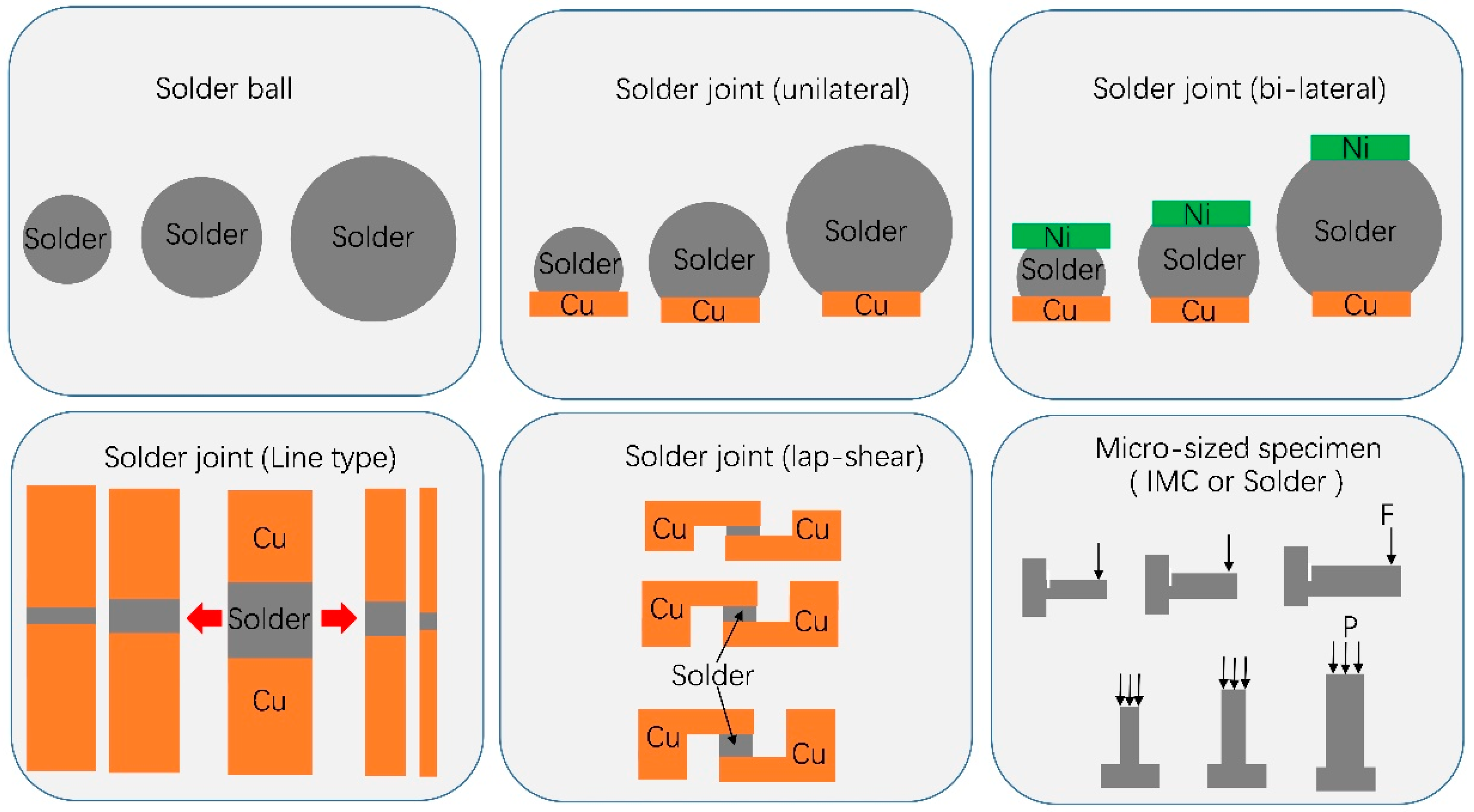
Different types of specimens have been used to investigate the size effects of solder joints, including solder balls, unilateral solder joints, bi-lateral solder joints, line-type solder joints, lap-shear solder joints, and micro-specimens, as summarized in Figure 1. Solder balls without substrate are usually used to investigate the thermal properties such as undercooling, solidification, and phase transformation. Unilateral solder joints are suitable to study the interfacial reaction and measure the IMC growth rate, as well as shear strength. The bi-lateral solder joint type is more approximate to the solder interconnects in packaging structures, and can be used to study the interfacial reaction with different substrates. The diameters of the solder balls and unilateral and bi-lateral solder joints usually range from 0.2 to 1.0 mm. Line-type and lap-shear solder joints are usually used to test the tensile and shear properties, respectively. Furthermore, there are two classes of line-type solder joints: One has a constant solder diameter but reducing solder height, and the other has a constant solder diameter-to-height ratio. The diameters of the Cu pillars of the line-type solder joints range from 300 μm to 2 mm, and the heights of solder layers range from 5 μm to 2 mm. Micro-sized specimens are fabricated by focused ion beam (FIB) milling, and can be utilized to explore the mechanical properties on the microscale and have received much more attention recently. For example, the fracture toughness of the IMC Cu6Sn5 can be obtained with the nanoindentation test on the microcantilever cylinder with a prefabricated notch. The microcantilever can be milled into a length of several microns, which is smaller than a single Cu6Sn5 grain. The depth of the notch can be milled to hundreds of nanometers. The compression test of Cu6Sn5 on the micron scale can also be conducted with FIB milling and nanoindentation. Wedge indenters are used in the microcantilever fracture test, while flat-end indenters are used in the compression test.
2. Size Effects on Microstructure in Solder Joints
2.1. IMC Formation and Growth
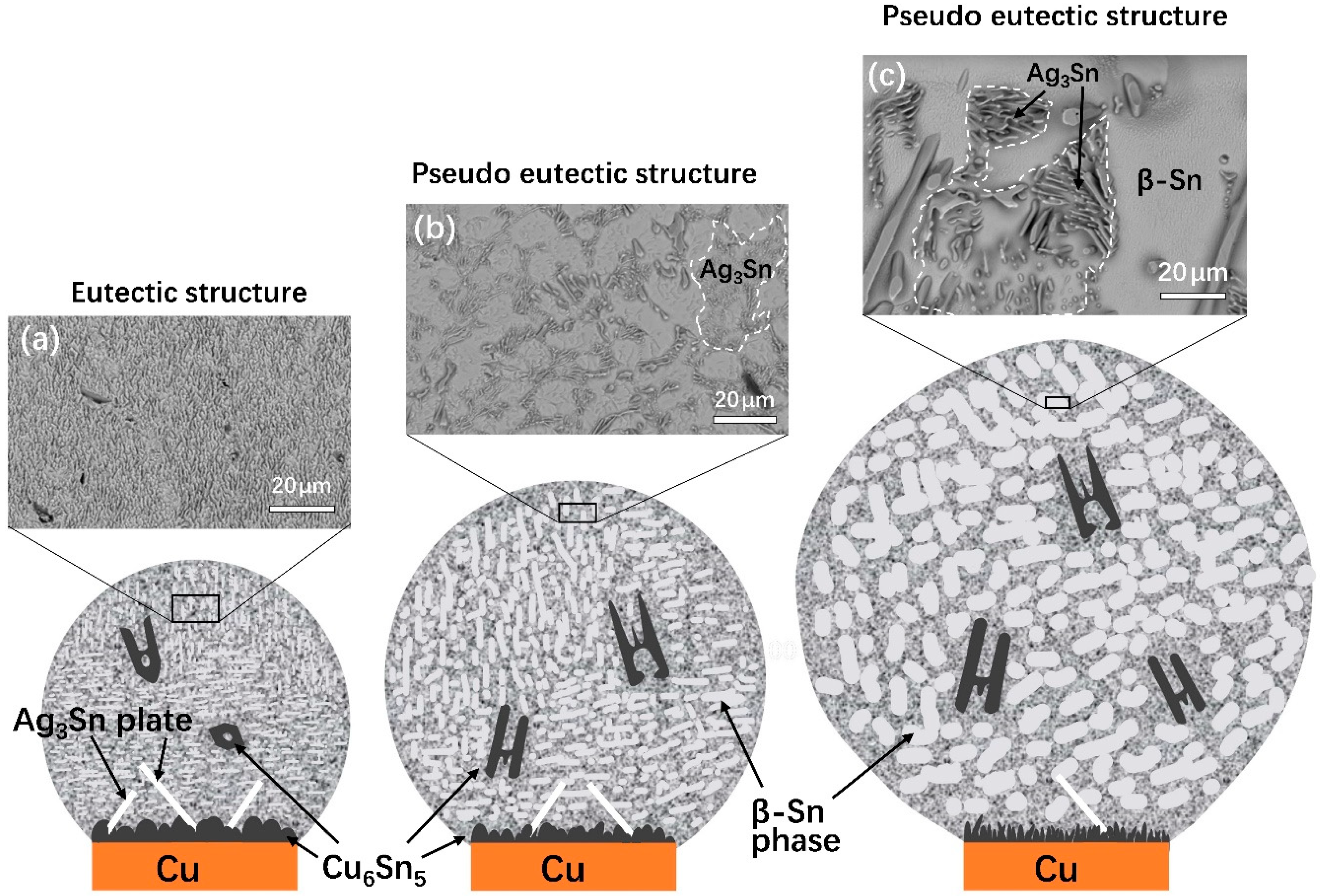
IMCs form during the reflow or thermal aging process in solder materials. Cu and Ni substrates are the most commonly used substrates in lead-free solder joints. For Cu-substrate solder joints, Cu6Sn5 and Cu3Sn are the major types of IMCs. As for Ni-substrate solder joints, Ni6Sn5 and Ni3Sn IMCs commonly occur at the Ni/Solder interface. Other types of substrate, such as Au/Ni–P/Cu (ENIG), Ag, Pa/Ti/Si, Co, Au, Fe, Cu–Mn, and Cu–Zn were summarized in Kotadia et al.’s study [10], while the IMCs formed during interfacial reactions in Sn–Ag–Cu solder joints of different substrates are listed in Table 1. IMCs act as the mechanical and electrical connections between the solder matrix and substrate. Therefore, the growth and evolution of IMC layers have a significant effect on the reliability of the solder joints [11,12]. The IMC growth corresponds to the Cu dissolution from substrate into the solder matrix, which is found to be greatly affected by the substrate area/solder volume ratio (V/A ratio) [9,13]. By taking the unilateral solder joints as an example, the size effects on the internal microstructure are shown in Figure 2. In general, the decreasing solder volume leads to the apparent coarsening of interfacial IMCs (i.e., Cu6Sn5 and Ag3Sn) and a finer dendritic β-Sn phase. The shapes and amount of precipitation (i.e., Cu6Sn5 and Ag3Sn) in the solder matrix formed in solidification are also dependent on the joint size. In eutectic structures, Ag3Sn dispersion in the solder alloy can increase the ductility. However, excessive thermal aging or multiple reflows can lead to plate-like Ag3Sn on the Cu6Sn5 IMCs. This plate-like Ag3Sn will increase the strain singularity near the interfacial layers of the solder joints. The solder joint size has significant effect on the eutectic structures in Sn–Ag–Cu solder joints. Dendritic Ag3Sn precipitation (see in the dashed lines) in the pseudo-eutectic structures also weaken the mechanical strength of the solder joints.
The IMC layer in a thinner or smaller solder joint is usually thicker than that in a solder joint with a larger volume. Lee et al. [27] studied the effect of gap size in solder joints on the microstructure at the interfaces of Ni/Sn/Cu and Cu/Sn/Cu using single-lap specimens, and showed that the gap size has a more significant effect on IMC thickness at the Ni/Sn interface than at the Cu/Sn interface. Park et al. [28] investigated the bump size and reflow time effects on the IMC thickness and growth rate. They found that the IMC layers in smaller Sn1.0Ag0.5Cu/Cu solder joints were thicker than those in larger solder joints after the initial reflow, but the IMC growth rate in smaller joints was slower than in larger solder joints during the second and third reflows. In contrast to the findings by Park et al. [28], Tian et al. [29] conducted thermal shock tests on Cu/Sn3.0Ag0.5/Ni solder joints with 100 and 200 μm pitches, and found that the IMC growth rates in the 100 μm pitch solder joints were obviously higher than those in joints with a 200 μm pitch. Studies of Cu/Sn/Cu under 160 °C solid-state thermal aging by Zhu et al. [30] indicated that the thickness effect of solder joints on the IMC growth rate was not that “the thinner the solder layer was, the faster the IMC grew” as usually believed. Instead, there was a threshold value of δ = 30 μm for solder thickness, and the initial growth rate of IMC in thinner solder joints (δ < 30 μm) was greater than that of thicker solder joints (δ > 30 μm), but the former decreased and the latter increased with an increasing aging time [30]. The size-dependent IMC growth rate was also reported by Wang et al. [31]. Based on both solid-state and liquid-state diffusions, they found that the commonly reported size-dependent IMC growth rate may be only valid under a liquid-state diffusion, but invalid under a solid-state diffusion.
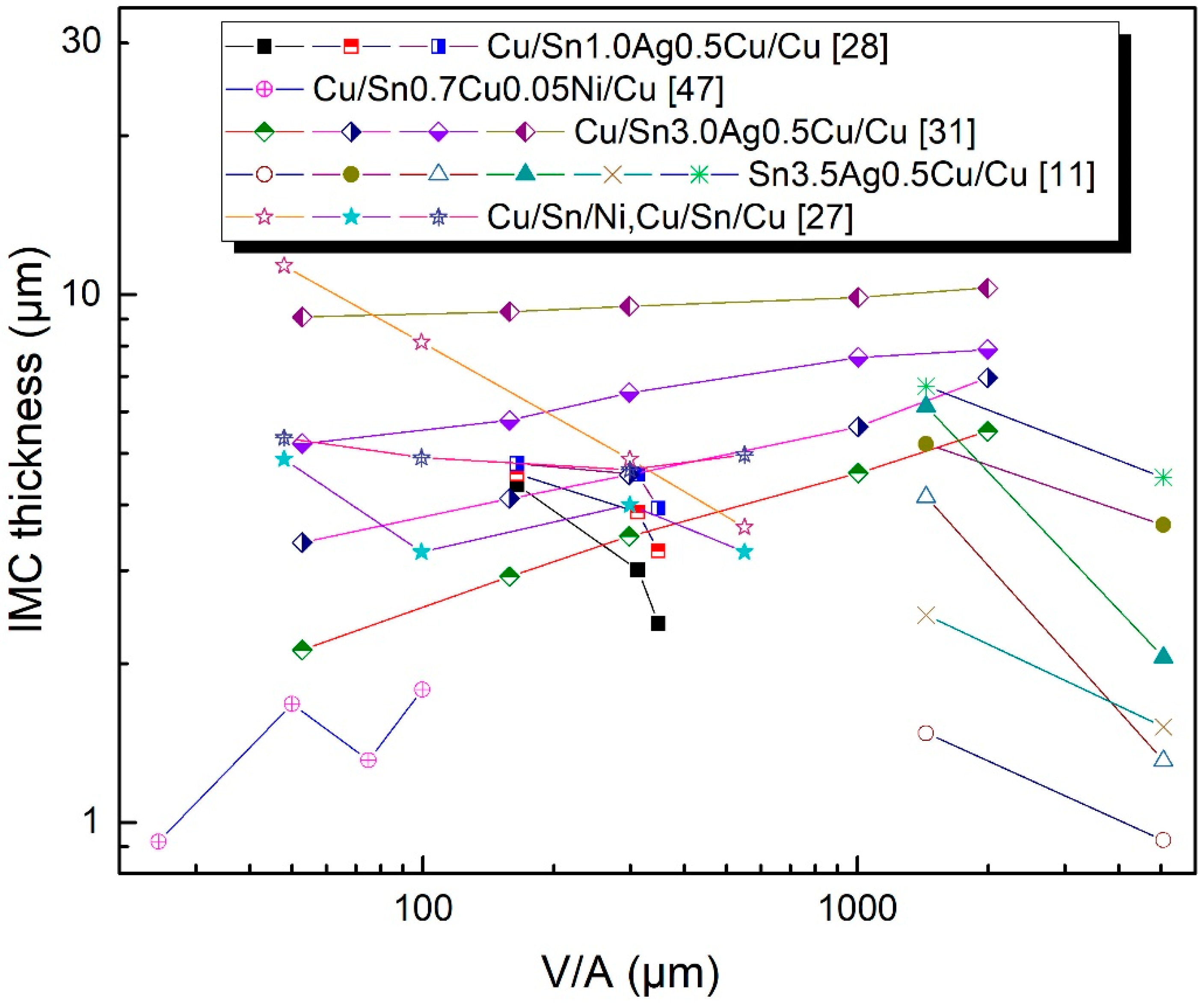
To obtain a more general relationship between solder joint size and IMC growth, the IMC thicknesses corresponding to solder joints with different ratios of solder volume to substrate area (V/A) are presented in Figure 3. It is observed that a linear relationship, as shown in Equation (1), seems to exist between the logarithmic IMC thickness and the V/A ratio, even though the slope of the linear fitting line can be positive or negative.
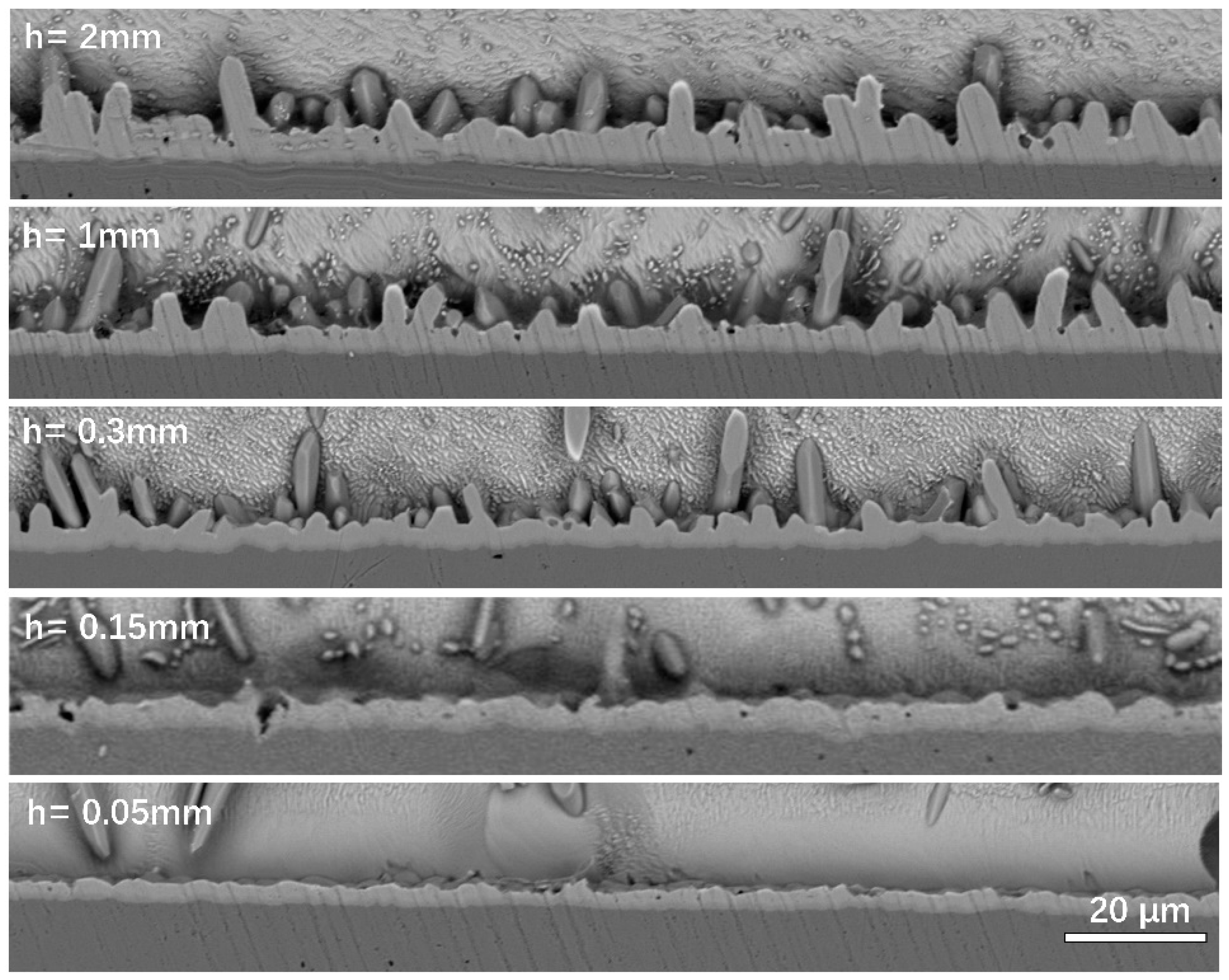
where r is the V/A ratio, t is the thickness of the IMC, t0 is related to the IMC thickness of the initial state, is a function related to the IMC growth rate, and the slope k depends on the specimen shape. Based on the data reviewed in Figure 3, a negative slope k usually occurs in line-type or bi-lateral solder joints, while unilateral solder joints always have a positive k value. Therefore, a constraint effect in line-type or bi-lateral solder joints, which slows down the IMC growth, is speculated to be the dominant mechanism for such a negative k value. The constraint effect on the IMC growth can be seen in Figure 4, where the solder joints with small gap sizes (50 and 150 μm) only form thin lamellar-type IMCs instead of scallop-type IMCs, which have been observed in the other three types of solder joint [31].
From the interaction point of view, the IMC growth rate is dominated by the Cu diffusion. Therefore, the underlying mechanism for the size effects of solder joints is highly likely to be related to the Cu flux. Abdelhadi et al. [32] established an analytical model to investigate the growth rate of Cu3Sn, which was found to be joint-size dependent and obey the parabolic relation with time. Huang et al. [33] measured the IMC evolution of Sn3.0Ag0.5Cu solder joints on Cu or Ni–P pads, and the Cu flux variation was inferred to be the cause of solder volume size effects. Li et al. [34] performed experiments and simulations regarding the Cu concentration effect on different sizes of Sn3.0Ag0.5C0.1TiO2/Cu solder joints, and concluded that the IMC formation may not simply obey diffusion-controlled or interfacial reaction-controlled growth, but was instead a combination of both. Compared with bulk diffusion, surface diffusion and intergranular diffusion are fast diffusion channels. Thus, one can infer that solder joints with a larger specific surface area tend to have a higher IMC growth rate under the same reflow or thermal conditions. Sun et al. [35] investigated the geometrical size effects on the interfacial IMC growth rate using wedge-shaped samples. Due to the higher IMC growth rate at the angle of the wedge than other districts, a salient triangle formed at the angle. Due to the significant solder volume to substrate surface area ratio in micro-bump solder joints, the IMC growth behavior could be controlled by the surface diffusion mechanism [36].
2.2. Solidification and Recrystallization in the Solder Matrix
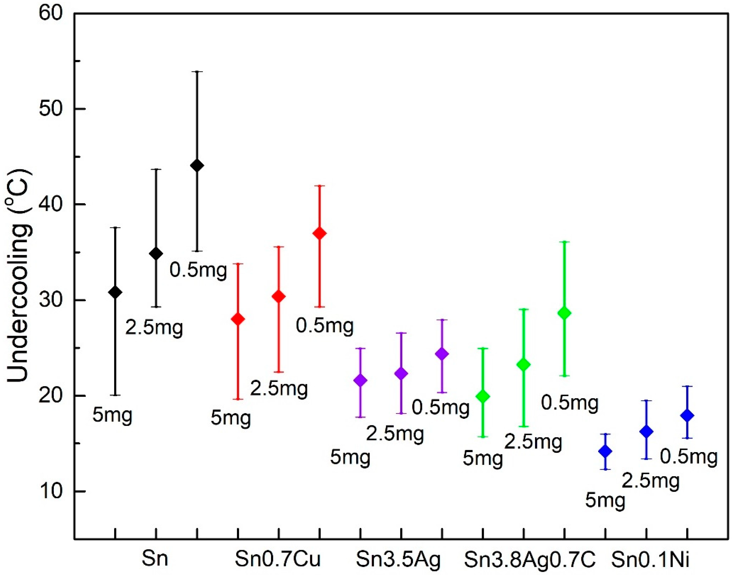
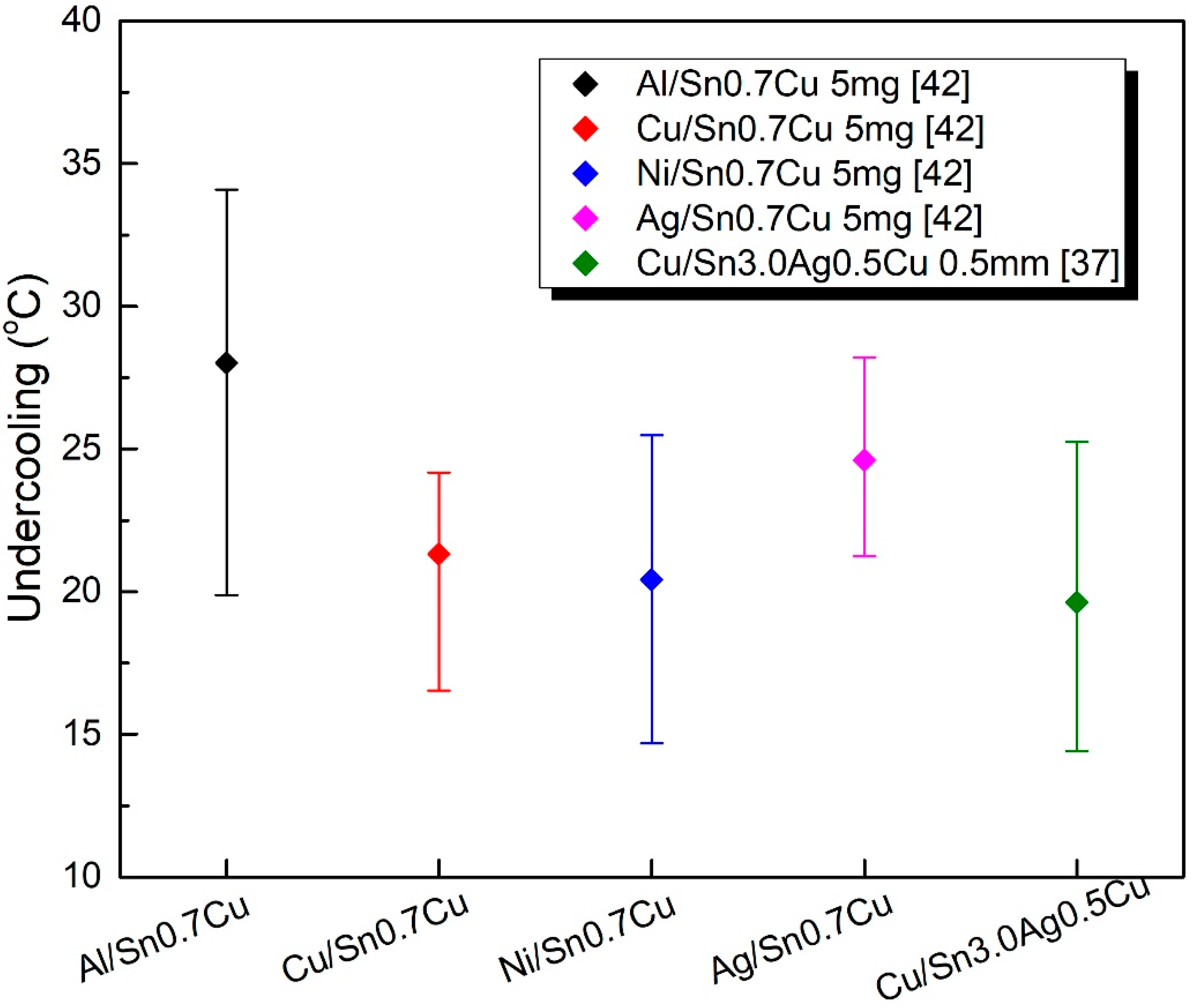
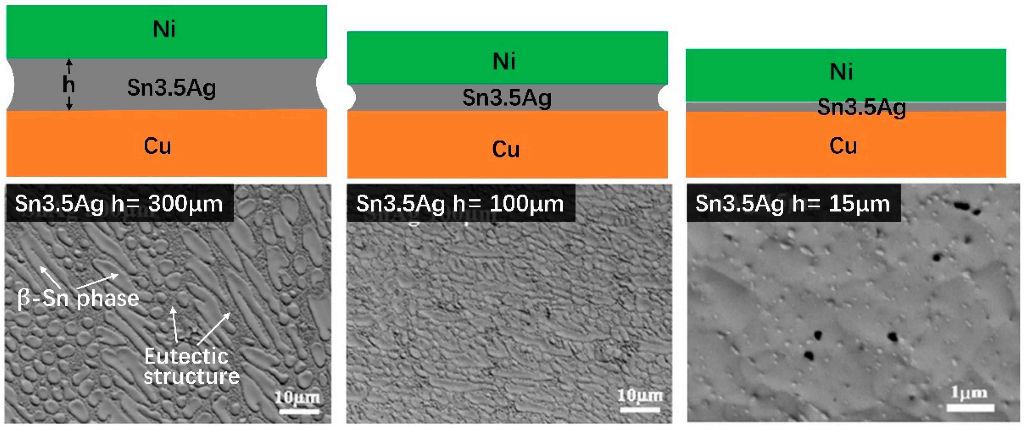
Apart from the interfacial microstructure, the solder size also has a crucial effect on the microstructure, including the β-Sn phase, eutectic phase, and bulk primary solidification phase in the solder matrix. The mechanical strength of solder balls is commonly regarded to be dependent on the microstructure size, while both the dendrite arm size and the eutectic phase size depend on the solder ball dimension. Furthermore, the microstructures in solder balls and solder joints are directly dependent on the solidification behavior in the annealing or reflow procedures [37,38,39]. Kinyanjui et al. [40] studied the undercooling behavior of Sn3.9Ag0.6Cu solder joints with diameters ranging between 200 to 2000 μm by differential scanning calorimetry (DSC) reflow tests, and reported a linear relationship between the undercooling temperature and inverse nominal diameter of the solder balls. Additionally, the dendrite arm sizes, which were approximately 0.008 times of the solder ball diameter, were found to be strongly size-dependent. Zhou et al. [41] investigated the increasing undercooling behavior of Sn3.0Ag0.5Cu solder balls and solder joints with diameters decreasing from 760 to 300 μm with DSC analysis. They found that the large primary solidification Ag3Sn phase had a large undercooling in the small solder balls, while the primary Cu6Sn5 phase formed in the solder joints. In addition, the grain size of the β-Sn phase was reported to be smaller, and the contained eutectic structure was observed to be less in the sample with small undercooling. Huang et al. [42] measured the size and substrate effects on the undercooling of solder alloys including Sn, Sn0.7Cu, Sn3.5Ag, Sn3.8Ag0.7Cu, and Sn0.1Ni, and found that the primary solidification phases of those solder alloys were β-Sn, Cu6Sn5, Ag3Sn, and Ni3Sn4, respectively. The primary solidification phase was illustrated to be the principle factor for the degrees of undercooling, followed by the substrate factor and solder ball size factor [42]. Solder volume and substrate effects on the undercooling of different types of solder alloy are summarized in Figure 5 and Figure 6, respectively.
The undercooling of solder joints depends on the solidification behavior. The effect of solder joint size on the solidification is intuitively depicted in Figure 2. For Sn3.0Ag0.5Cu solder joints with a 200 μm diameter, the β-Sn phase in Figure 2a is relatively small compared with that in Figure 2b,c. As the solder joints’ diameters increase to 500 and 760 μm, the eutectic structures transform to pseudo-eutectic structures, which means that Ag3Sn and Cu6Sn5 phases precipitate during the solidification.
Based on the classic solidification theory, the relationship between solder size and undercooling can be described as follows [41]:
where d is the diameter of the solder ball, ΔT is the degree of undercooling, and Ts and Tm are the theoretical solidification and melting temperature, respectively. Additionally, r is the cooling rate, Ks depends on the atoms’ vibration frequency, γsl is the crystal–liquid interfacial energy, Lν is the melting enthalpy per volume, and f(θ) is dependent on the catalytic potency. For small solder bumps, the driving force for solidification is usually larger than big bumps, which leads to the stronger undercooling. Furthermore, smaller solder bumps are apt to bear more severe temperature gradients, which also promotes the rapid cooling and enhances the undercooling phenomenon. As the main intermetallic compounds in the solder matrix, Ag3Sn particles in Sn–Ag alloy solder joints are part of the significant hardening phase, but the related studies are relatively exiguous. Ma et al. [43] studied the size effects on Ag3Sn intermetallic growth in Sn3.5Ag solder joints during reflows, and the size of Ag3Sn particles was observed to increase with the increase of the solder ball diameter.
3. Size Effects on Mechanical Properties of Solder Joints
Mechanical properties of the solder joints can be affected by not only the macro-geometry size-induced constraints but also the microstructural size-induced enhancement. What makes the size effects more intricate is that the microstructural size, such as for the β-Sn phase, is also affected by the macro-geometry of the solder joints. For example, for the bump size effect on solder hardening, the creep resistance and hardness of Sn3.0Ag0.5Cu and Sn3.5Ag solder joints are illustrated to be increasing with the decrease of bump height. Meanwhile, the secondary β-Sn dendrite arm length was found to be linear with respect to the logarithm of the bump height [44], as shown in Figure 7. Apart from the size effects on intrinsic mechanical properties of the solder matrix, local mechanical behavior of IMCs was also reported to be size-dependent. Higher hardness and elastic modulus were observed in smaller Sn3.5Ag/Cu solder joints by the nanoindentation method [45]. Therefore, simple conclusions related to size effects on mechanical behavior are difficult to arrive at, but the transition or tendency of mechanical properties under certain circumstances are meaningful for the exploration of underlying mechanisms of size effects on the mechanical properties of solder joints.
3.1. Tensile Behavior of Solder Joint
With the decreasing bump height, the transition of the failure mode from ductile fractures in solder to brittle fractures along IMCs was reported in tensile tests [46]. It is noted that Cu pillar micro-bump solder joints are an important type of interconnection in 3D electronic packaging. Researches usually employ the line-type specimen to investigate the properties of Cu pillar micro-bump solder joints, with different solder heights which range from 5 to 60 μm, such as in Wang et al.’s study [46]. When the solder height of the micro-bump solder joint drops to 10 μm or less, the whole solder alloy has the potential to transform into IMCs. Then, Cu/IMC/Cu or Ni/IMC/Cu solder joints will occur. Apart from the brittle IMCs, micro-cracks due to Kirkendall voids will bring reliability challenges. More elaborate properties on Cu pillar micro-bump solder joints were summarized by Tu et al. [1]. Li et al. [47] investigated the joint gap size effects on the tensile properties of Cu/Sn0.7Cu0.05Ni/Cu solder joints by experiments and simulations. Wang et al. [31] conducted tensile tests on Cu/Sn3.0Ag0.5Cu/Cu solder joints with gap sizes ranging from 50 to 2000 μm, and they found that the tensile strength increased as the joint gap decreased, and the stress triaxiality was used to explain the higher strength of joints with smaller gaps. Qin et al. [48] performed microscale tensile tests of Ni/Sn3.0Ag0.5Cu/Ni and Cu/Sn3.0Ag0.5Cu/Cu solder joints with thickness-to-diameter ratios (R) from 1/3 to 1/12 by a dynamic mechanical analyzer (DMA). Both tensile strength and fracture mode were dependent on R, and the damage-equivalent stress, which is deemed as a suitable criterion in evaluating the strength and damage of the joints by the finite element method, showed a decreasing trend with the decrease of the R value. In addition to the typical gap size effects on solder joint behavior, void formation in the solder joints during flux outgassing was found to enhance the ductility of the Cu/Sn3.5Ag0.75Cu/Cu solder joints in tensile tests. This effect was significantly more obvious in joints with larger solder gaps [49]. For an ideal rigid plastic body, the geometry effect on fracture strength σF of the solder joint was suggested as:
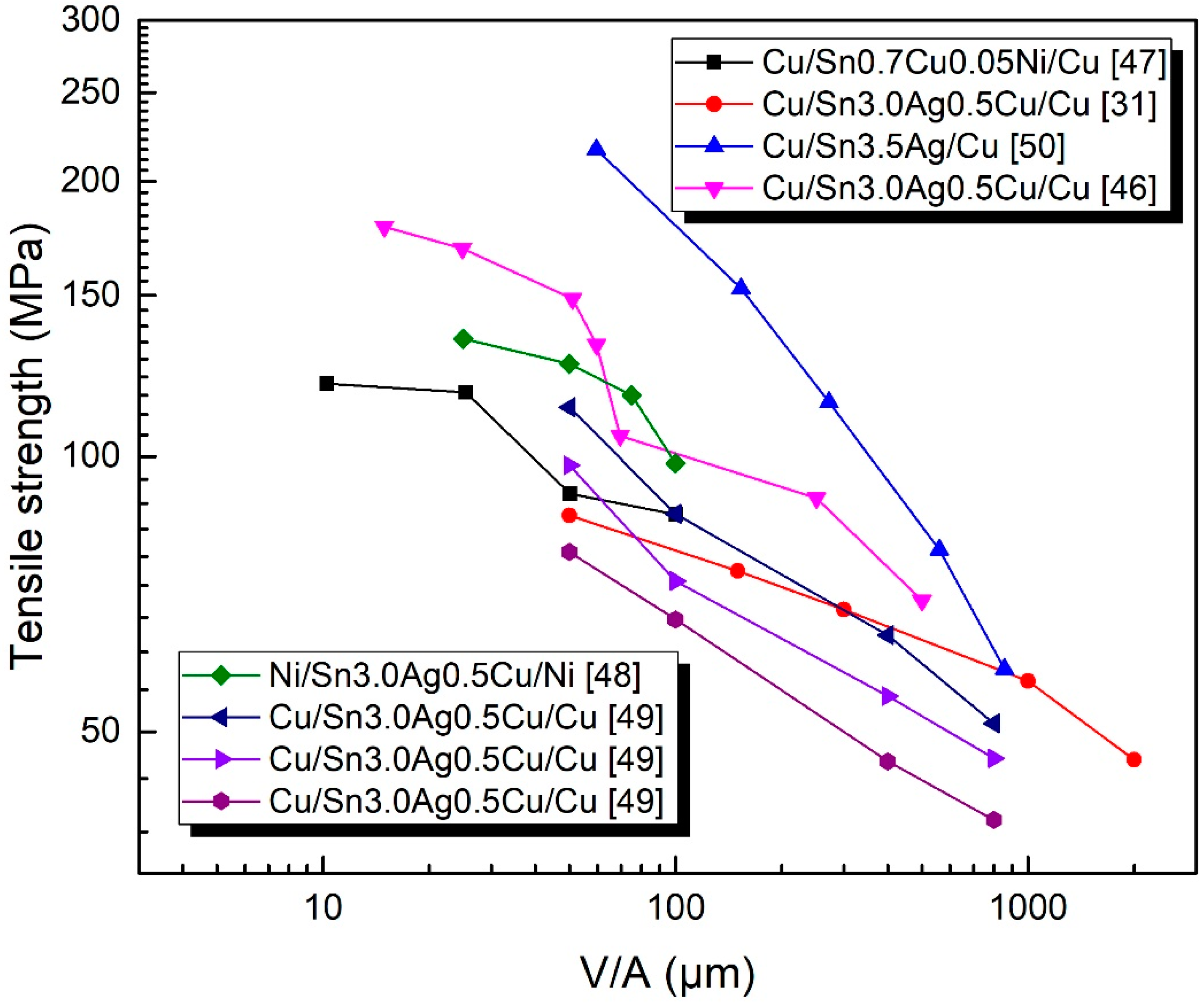
where σyield is the yield strength of the solder material, and h and d are the solder thickness and substrate diameter, respectively. However, the ideal rigid plasticity is a strong assumption, especially when h approaches d. Tensile strengths of different types of solder joints are summarized in Figure 8. A linear relationship between the logarithmic tensile strength and the logarithmic V/A is found. As noticed for the data from Hutter et al. and Kim et al.’s studies [24,26] which are not well-appropriated by linear fitting, this may be due to the significantly slower loading rate, which leads to creep failure [26], and also the excessive IMC growth in solder joints with small V/A ratios, which leads to failure mechanism transition [24].
Zimprich et al. [50] evaluated the mechanical size effects of Cu/Sn3.5Ag/Cu solder joints with gap sizes ranging from 25 to 850 μm by the Orowan model. Based on a constraint mechanism that enhanced the shear strength and was different from that in tensile specimen, they also pointed out that the constraint effect which enhanced the ultimate tensile and yield strengths was only dominant for gap sizes below 200 μm. The IMC effect on the mechanical strength, as found in Zimprich’s research [50], does not seem obvious. However, when the IMCs occupy a significant portion of the whole solder joint, the IMC effect cannot be neglected. Mo et al. [51] performed finite element simulations to investigate the size dependency of solder joints formed only by IMC, and found that the stress concentration was more significant due to the absence of the ‘relief’ effect of bulk solder joints (the ‘relief’ effect refers to the ductility of the solder alloy, which can blunt the crack front and relieve the stress singularity). Wang et al. [52] investigated the solder volume, aging, and reflow effects on the shear strength of Sn3.0Ag0.5Cu/Cu solder joints, and they found that reflow times had a tiny influence on the shear strength because reflow mainly increased the interfacial IMCs but did not alter the microstructure in solder layers. Chen et al. [53] used the lap-shear specimen to measure the shear strength of Cu/Sn/Cu and FeNi/Sn/FeNi solder joints. In their experiment, Sn grain size was observed to enlarge with the decreasing of solder thickness, thus explaining the unusual relationship between shear strength and solder thickness.
Shear strengths of different kinds of solder joints are summarized in Table 2. Compared with the tensile strengths in Figure 8, most of the reviewed data in Table 2 show milder decreasing tendencies with the increase of the V/A ratio, except the data from Zimprich et al.’s study [50] which indicated a different mechanism of mechanical constraint between shear and tensile specimens. Of course, the deformation mechanisms between shear and tensile specimens are different, and thus different stresses and displacement singularities at the joint corners are found. With the theoretical analysis on the singularities of solder joint corners, the constraint differences between tensile and shear specimens can be expected to be revealed.
Size effects on the strength of solder joints are not always “smaller-being-stronger”. Instead, under certain circumstances, the “smaller-being-weaker” phenomenon can occur as well. Gan et al. [54] reported an unusual size effect on the strength of Sn/Pb solder joints with fine lamellar phases, in which both micropillars compression tests and dislocation modeling were employed to analyze the decreasing strength with the specimen size. It was reported that there were fewer interphase boundaries in smaller sized specimens, which blocked the dislocation and thus led to the lower mechanical strength.
3.2. Fracture and Creep Deformation of Solder Joints
Li et al. [55] investigated size and constraint effects on the fracture behavior of Sn3.0Ag0.5Cu and Sn37Pb solder joints by simulations with elastic–plastic and dynamic fracture methods. The damage-equivalent stress area and energy release distribution, which strongly depend on the diameter-to-thickness ratio (d/t) of the solder joints, were used to characterize the fracture mechanism and position. They found that the solder joints with a small d/t were apt to fracture at the middle of the solder layer, while the joints with a large d/t tended to fracture at the solder/IMC interface. Wang et al. [56] developed a theoretical model based on the local stress singularity at the bi-material corner to analyze the relationship between the microstructure size and macro-fracture toughness of lead-free solder joints. The IMC grain size effect on the fracture toughness of solder joints was stated as follows [34]:
where KQ is the predicted interfacial fracture toughness and d is the representative length of the interfacial IMC grain. The parameters K0Q and d0, which are dependent on the specimen material and geometry, can be obtained by numerical fitting. The parameters λIMC and λs, which can be theoretically and numerically determined, are the order of displacement singularity at the corner of the IMC grain and the solder joint, respectively. This size effect was suggested to be valid in solder joints with scallop-type IMCs [56,57,58,59], as shown in Figure 9.
Size effects on the creep deformation of line-type Cu/Sn3.0Ag0.5Cu/Cu solder joints were studied by Li et al. [60] using DMA. They found that the creep exponents ranged from 4.2 to 3.1 and the creep activation energy varied from 90 to 66 kJ/mol as the joint thickness increased from 50 to 200 μm. Lattice diffusion was deemed to be the dominant creep mechanism, since the creep exponents were closed to the theoretical exponents of lattice diffusion. The findings by Li et al. [60] are in accordance with the bump height effect on solder hardening [44].
Size effects on solder joints are usually complicated in terms of various compositions and microstructures. Therefore, a multi-scale microstructure-based modeling method, which can capture the hardening and aging effects of mixed intermetallic phases on the constitutive behavior, is becoming an important approach for exploring the relationship between the microstructure and mechanical behavior of solder joints [61]. However, so far the multi-scale modeling method is only appropriate in simulating the mechanical behavior of solder layers which incorporate fine intermetallic particles. When a relatively weak interface strength is referred to, this method may not be applicable.
4. Conclusions
The characteristics of both microstructures (interfacial IMC layers, precipitation, eutectic structures, and β-phases in the solder matrix) and mechanical properties (tensile strength, shear and compression, fracture, and creep deformation) of different-sized solder joints were summarized in this review. Though there were many researches on the size effects of solder joints, some issues are still expected to be further explored and elucidated:
- Fatigue properties of different scales of solder joints are relatively scarce. Due to different microstructures and stress singularities, crack initiation and propagation behaviors of micro-bump solder joints can be quite different from the bulk solder joints.
- A multi-scale microstructure-based modeling method is urgently required to predict the mechanical behaviors of solder joints with different sizes. Modeling based on the microstructure distribution and evolution can capture the local characteristics with reasonable accuracy, and thus is more convincing than the homogenization model.
- Defects evolve in different sizes of solder joints. Defects such as Kirkendall voids form in the Cu3Sn layer and can have important effects on the mechanical reliability of solder joints. Research on the dislocation motivations under different loadings and the dislocation density transition in different-sized solder joints are also important for understanding the size effects.
- The differences of the constraint mechanism between shear and tensile specimens are still not clear and need further investigations.
Author Contributions
S.W. and X.L. conceived and drafted the review; S.W. performed the literature review; X.L., Y.Y. and S.W. discussed the paper frame.
Funding
This research was funded by the National Natural Science Foundation of China (grant number 51508464), the Natural Science Foundation of Shaanxi Province (grant number 2017JM1013), the Astronautics Supporting Technology Foundation of China (grant number 2019-HT-XG), and the Fundamental Research Funds for the Central Universities (grant number 3102018ZY015).
Conflicts of Interest
The authors declare no conflict of interest.
References
- Tu, K.N. Reliability challenges in 3D IC packaging technology. Microelectron. Reliab. 2011, 51, 517–523. [Google Scholar] [CrossRef]
- Ladani, L.J. Numerical analysis of thermo-mechanical reliability of through silicon vias (TSVs) and solder interconnects in 3-dimensional integrated circuits. Microelectron. Eng. 2010, 87, 208–215. [Google Scholar] [CrossRef]
- Liu, Y.; Chu, Y.-C.; Tu, K.N. Scaling effect of interfacial reaction on intermetallic compound formation in Sn/Cu pillar down to 1 μm diameter. Acta Mater. 2016, 117, 146–152. [Google Scholar] [CrossRef]
- Zhang, L.; Tu, K.N. Structure and properties of lead-free solders bearing micro and Nano particles. Mater. Sci. Eng. 2014, 82, 1–32. [Google Scholar] [CrossRef]
- Tsao, L.C.; Chang, S.Y. Effects of Nano-TiO2 additions on thermal analysis, microstructure and tensile properties of Sn3.5Ag0.25Cu solder. Mater. Des. 2010, 31, 990–993. [Google Scholar] [CrossRef]
- Gain, A.K.; Zhang, L.; Quadir, M.Z. Thermal aging effects on microstructures and mechanical properties of an environmentally friendly eutectic tin-copper solder alloy. Mater. Des. 2016, 110, 275–283. [Google Scholar] [CrossRef]
- Gain, A.K.; Zhang, L. Microstructure, thermal analysis and damping properties of Ag and Ni nano-particles doped Sn–8Zn–3Bi solder on OSP–Cu substrate. J. Alloys Compd. 2014, 617, 779–786. [Google Scholar] [CrossRef]
- Liu, S.; McDonald, S.; Sweatman, K.; Nogita, K. The effects of precipitation strengthening and solid solution strengthening on strain rate sensitivity of lead-free solders: Review. Microelectron. Reliab. 2018, 84, 170–180. [Google Scholar] [CrossRef]
- Yin, L.; Li, W.; Wei, S.; Xu, Z. Size and volume effects in microscale solder joint of electronic packaging. In Proceedings of the 12th International Conference on Electronic Packaging Technology and High Density Packaging, Shanghai, China, 8–11 August 2011; pp. 832–834. [Google Scholar]
- Kotadia, H.R.; Howes, P.D.; Mannan, S.H. A review: On the development of low melting temperature Pb-free solders. Microelectron. Reliab. 2014, 54, 1253–1273. [Google Scholar] [CrossRef]
- Islam, M.N.; Sharif, A.; Chan, Y.C. Effect of volume in interfacial reaction between eutectic Sn-3.5% Ag-0.5% Cu solder and Cu metallization in microelectronic packaging. J. Electron. Mater. 2005, 34, 143–149. [Google Scholar] [CrossRef]
- Arzt, E.J.A.M. Size effects in materials due to microstructural and dimensional constraints: A comparative review. Acta Mater. 1998, 46, 5611–5626. [Google Scholar] [CrossRef]
- Chang, C.C.; Kao, C.R. Dissolution and interfacial reaction between Cu and Sn-Ag-Cu solders. In Proceedings of the International Microsystems, Packaging, Assembly and Circuits Technology, Taipei, Taiwan, 1–3 October 2007; pp. 54–57. [Google Scholar]
- Laurila, T.; Vuorinen, V.; Kivilahti, J.K. Interfacial reactions between lead-free solders and common base materials. Mater. Sci. Eng. 2005, 49, 1–60. [Google Scholar] [CrossRef]
- Abtew, M.; Selvaduray, G. Lead-free Solders in Microelectronics. Mater. Sci. Eng. 2000, 27, 95–141. [Google Scholar] [CrossRef]
- Wang, J.; Zhang, L.G.; Liu, H.S.; Liu, L.B.; Jin, Z.P. Interfacial reaction between Sn–Ag alloys and Ni substrate. J. Alloys Compd. 2008, 455, 159–163. [Google Scholar] [CrossRef]
- Moon, K.W.; Boettinger, W.J.; Kattner, U.R.; Biancaniello, F.S.; Handwerker, C.A. Experimental and thermodynamic assessment of Sn-Ag-Cu solder alloys. J. Electron. Mater. 2000, 29, 1122–1136. [Google Scholar] [CrossRef] [Green Version]
- He, M.; Lau, W.H.; Qi, G.; Chen, Z. Intermetallic compound formation between Sn–3.5Ag solder and Ni-based metallization during liquid state reaction. Thin Solid Films 2004, 462–463, 376–383. [Google Scholar] [CrossRef]
- Wu, R.W.; Tsao, L.C.; Chang, S.Y.; Jain, C.C.; Chen, R.S. Interfacial reactions between liquid Sn3.5Ag0.5Cu solders and Ag substrates. J. Mater. Sci. 2011, 22, 1181–1187. [Google Scholar] [CrossRef]
- Kim, T.H.; Kim, Y.-H. Sn-Ag-Cu and Sn-Cu solders: Interfacial reactions with platinum. JOM 2004, 56, 45–49. [Google Scholar] [CrossRef] [Green Version]
- Wang, C.-H.; Kuo, C.-Y. Coupling Effect of the Interfacial Reaction in Co/Sn/Cu Diffusion Couples. J. Electron. Mater. 2010, 39, 1303–1308. [Google Scholar] [CrossRef]
- Zhu, W.; Wang, J.; Liu, H.; Jin, Z.; Gong, W. The interfacial reaction between Sn–Ag alloys and Co substrate. Mater. Sci. Eng. A 2007, 456, 109–113. [Google Scholar] [CrossRef]
- Lee, T.K.; Zhang, S.; Wong, C.C.; Tan, A.C.; Hadikusuma, D. Interfacial microstructures and kinetics of Au/SnAgCu. Thin Solid Films 2006, 504, 441–445. [Google Scholar] [CrossRef]
- Hutter, M.; Schmidt, R.; Zerrer, P.; Rauschenbach, S.; Wittke, K.; Scheel, W.; Reichl, H. Effects of additional elements (Fe, Co, Al) on SnAgCu solder joints. In Proceedings of the 2009 59th Electronic Components and Technology Conference, San Diego, CA, USA, 26–29 May 2009; pp. 54–60. [Google Scholar]
- Tseng, C.-F.; Wang, K.-J.; Duh, J.-G. Interfacial Reactions of Sn-3.0Ag-0.5Cu Solder with Cu-Mn UBM During Aging. J. Electron. Mater. 2010, 39, 2522–2527. [Google Scholar] [CrossRef]
- Kim, Y.M.; Roh, H.-R.; Kim, S.; Kim, Y.-H. Kinetics of Intermetallic Compound Formation at the Interface Between Sn-3.0Ag-0.5Cu Solder and Cu-Zn Alloy Substrates. J. Electron. Mater. 2010, 39, 2504–2512. [Google Scholar] [CrossRef]
- Lee, G.; Song, J.; Lae, Y.; Chiu, Y.; Su, C. Size and substrate effects on microstructure and shear properties of solder joints. In Proceedings of the 10th International Conference on Electronic Materials and Packaging, (EMAP 2008), Taipei, Taiwan, 22–24 October 2008; pp. 187–190. [Google Scholar]
- Park, Y.; Kwon, Y.; Moon, J.; Lee, Y.; Lee, J.; Paik, K. Effects of fine size lead-free solder ball on the interfacial reactions and joint reliability. In Proceedings of the 11th Electronic Packaging Technology Conference (EPTC 2009), Singapore, 9–11 December 2009; pp. 321–324. [Google Scholar]
- Tian, Y.; Liu, X.; Chow, J.; Wu, Y.P.; Sitaraman, S.K. Comparison of IMC growth in flip-chip assemblies with 100 and 200 μm pitch SAC305 solder joints. In Proceedings of the IEEE 63rd Electronic Components and Technology Conference (ECTC 2013), Las Vegas, NV, USA, 28–31 May 2013; pp. 1005–1009. [Google Scholar]
- Zhu, Y.; Sun, F. Effect of solder joint thickness on intermetallic compound growth rate of Cu/Sn/Cu solder joints during thermal aging. J. Electron. Packag. 2016, 138, 041005. [Google Scholar] [CrossRef]
- Wang, S.; Yao, Y.; Long, X. Size effect on microstructure and tensile properties of Sn3.0Ag0.5Cu solder joints. J. Mater. Sci. 2017, 28, 17682–17692. [Google Scholar] [CrossRef]
- Abdelhadi, O.M.; Ladani, L. Effect of joint size on microstructure and growth kinetics of intermetallic compounds in solid-liquid interdiffusion Sn3.5Ag/Cu-substrate solder joints. J. Electron. Packag. 2013, 135, 021004. [Google Scholar] [CrossRef]
- Huang, M.L.; Yang, F. Size effect on interfacial reactions of Sn3.0Ag0.5Cu solder balls on Cu and NiP pads. J. Mater. Sci. 2014, 26, 933–942. [Google Scholar]
- Li, Z.L.; Li, G.Y.; Li, B.; Cheng, L.X.; Huang, J.H.; Tang, Y. Size effect on IMC growth in micro-scale Sn-3.0Ag-0.5Cu-0.1TiO2 solder joints in reflow process. J. Alloys Compd. 2016, 685, 983–991. [Google Scholar] [CrossRef]
- Sun, X.; Sun, F.; Liu, Y. Geometrical size effect on interfacial diffusion of solder joint. In Proceedings of the International Symposium on Advanced Packaging Materials (APM 2011), Xiamen, China, 25–28 October 2011; pp. 242–245. [Google Scholar]
- Zhou, M.; Zhao, X.; Yue, W.; Ke, C.; Zhang, X. Size and boundary effects on the growth and morphology evolution of interfacial intermetallic compound of Sn0.3Ag0.7Cu/Cu micro-bump joints. In Proceedings of the 18th International Conference on Electronic Packaging Technology (ICEPT 2017), Harbin, China, 16–19 August 2017; pp. 1667–1671. [Google Scholar]
- Zhou, M.B.; Ma, X.; Zhang, X.P. Undercooling Behavior and Solidification Microstructure Evolution of Sn-Cu-Ni Solders Modified by Minute Amount of Mixed Rare Earth La-Ce. In Materials Science Forum; Trans Tech Publications: Princeton, NJ, USA, 2010; pp. 1373–1376. [Google Scholar]
- Kang, J.; Conrad, H. Microstructure coarsening during static annealing of 60Sn40Pb solder joints: II eutectic coarsening kinetics. J. Electron. Mater. 2001, 30, 1303–1307. [Google Scholar]
- Huang, Y.C.; Chen, S.W. Effects of Co Alloying and Size on Solidification and Interfacial Reactions in Sn-57 wt.%Bi-(Co)/Cu Couples. J. Electron. Mater. 2011, 40, 62–70. [Google Scholar] [CrossRef]
- Kinyanjui, R.; Lehman, L.P.; Zavalij, L.; Cotts, E. Effect of Sample Size on the Solidification Temperature and Microstructure of SnAgCu Near Eutectic Alloys. J. Mater. Res. 2005, 20, 2914–2918. [Google Scholar] [CrossRef]
- Zhou, M.; Xiao, M.; Zhang, X. Size effect on the intermetallic compound coalescence in Sn-Ag-Cu solder and Sn-Ag-Cu/Cu solder joints. In Proceedings of the 2011 12th International Conference on Electronic Packaging Technology and High Density Packaging (ICEPT-HDP 2011), Shanghai, China, 8–11 August 2011; pp. 248–253. [Google Scholar]
- Huang, Y.C.; Chen, S.W.; Wu, K.S. Size and Substrate Effects upon Undercooling of Pb-Free Solders. J. Electron. Mater. 2010, 39, 109–114. [Google Scholar] [CrossRef]
- Ma, H.; Kunwar, A.; Huang, R.; Chen, J.; Wang, Y.; Zhao, N.; Ma, H. Size effect on IMC growth induced by Cu concentration gradient and pinning of Ag3Sn particles during multiple reflows. Intermetallics 2017, 90, 90–96. [Google Scholar] [CrossRef]
- Ho, C.; Tsai, M.; Duh, J.; Lee, J. Bump height confinement governed solder alloy hardening in Cu/SnAg/Ni and Cu/SnAgCu/Ni joint assemblies. J. Alloys Compd. 2014, 600, 199–203. [Google Scholar] [CrossRef]
- Ladani, L.; Abdelhadi, O. Structural size effect on mechanical behavior of intermetallic material in solder joints: Experimental investigation. J. Electron. Packag. 2014, 137, 014501. [Google Scholar] [CrossRef]
- Wang, Y.; De Rosa, I.M.; Tu, K.N. Size effect on ductile-to-brittle transition in Cu-solder-Cu micro-joints. In Proceedings of the 65th IEEE Electronic Components and Technology Conference (ECTC 2015), San Diego, CA, USA, 26–29 May 2015; pp. 632–639. [Google Scholar]
- Li, W.; Zhou, M.; Qin, H.; Ma, X.; Zhang, X. Experimental and numerical study of the size effect on microstructure and mechanical behavior of Cu/Sn0.7Cu0.05Ni/Cu joints with very small solder volume. In Proceedings of the 13th International Conference on Electronic Packaging Technology and High Density Packaging (ICEPT-HDP 2012), Guilin, China, 13–16 August 2012; pp. 749–754. [Google Scholar]
- Qin, H.B.; Zhang, X.P.; Zhou, M.B.; Zeng, J.B.; Mai, Y.W. Size and constraint effects on mechanical and fracture behavior of micro-scale Ni/Sn3.0Ag0.5Cu/Ni solder joints. Mater. Sci. Eng. A 2014, 617, 14–23. [Google Scholar] [CrossRef]
- Magnien, J.; Khatibi, G.; Lederer, M.; Ipser, H. Investigation of interfacial behavior in miniaturized solder interconnects. Mater. Sci. Eng. A 2016, 673, 541–550. [Google Scholar] [CrossRef]
- Zimprich, P.; Saeed, U.; Betzwar-Kotas, A.; Weiss, B.; Ipser, H. Mechanical size effects in miniaturized lead-free solder joints. J. Electron. Mater. 2008, 37, 102–109. [Google Scholar] [CrossRef]
- Mo, L.; Wu, F.; Liu, C.; Xia, W. The size dependency of full IMC solder joint for 3D interconnection. In Proceedings of the 2012 IEEE 62nd Electronic Components and Technology Conference (ECTC 2012), San Diego, CA, USA, 29 May–1 June 2012; pp. 839–843. [Google Scholar]
- Wang, C.; Wang, X.; Tian, Y. Volume effect on shear strength of SnAgCu lead-free solder joints. Trans. China Weld. Inst. 2011, 32, 1–4. [Google Scholar]
- Chen, C.; Zhang, L.; Zhao, J.X.; Cao, L.H.; Shang, J.K. Gap Size Effects on the Shear Strength of Sn/Cu and Sn/FeNi Solder Joints. J. Electron. Mater. 2012, 41, 2487–2494. [Google Scholar] [CrossRef]
- Gan, K.F.; Ngan, A.H.W. The unusual size effect of eutectic Sn/Pb alloys in the micro regime: Experiments and modeling. Acta Mater. 2018, 151, 282–292. [Google Scholar] [CrossRef]
- Li, B.; Zhang, X.P.; Yang, Y.; Yin, L.M.; Pecht, M.G. Size and constraint effects on interfacial fracture behavior of microscale solder interconnects. Microelectron. Reliab. 2013, 53, 154–163. [Google Scholar] [CrossRef]
- Wang, S.; Yao, Y.; Wang, W. Microstructure and size effect of interfacial intermetallic on fracture toughness of Sn3.0Ag0.5Cu solder interconnects. Eng. Fract. Mech. 2018, 202, 259–274. [Google Scholar] [CrossRef]
- Nadimpalli, S.P.V.; Spelt, J.K. R-curve behavior of Cu–Sn3.0Ag0.5Cu solder joints: Effect of mode ratio and microstructure. Mater. Sci. Eng. A 2010, 527, 724–734. [Google Scholar] [CrossRef]
- Huang, Z.; Kumar, P.; Dutta, I.; Pang, J.H.L.; Sidhu, R.; Renavikar, M.; Mahajan, R. Fracture of Sn-Ag-Cu Solder Joints on Cu Substrates: I. Effects of Loading and Processing Conditions. J. Electron. Mater. 2012, 41, 375–389. [Google Scholar] [CrossRef]
- Hayes, S.M.; Chawla, N.; Frear, D.R. Interfacial fracture toughness of Pb-free solders. Microelectron. Reliab. 2009, 49, 269–287. [Google Scholar] [CrossRef]
- Li, W.; Cao, S.; Zhang, X. Size effect on creep deformation and fracture behavior of micro-scale Cu/Sn-3.0Ag-0.5Cu/Cu solder joints. In Proceedings of the 17th International Conference on Electronic Packaging Technology (ICEPT 2016), Wuhan, China, 16–19 August 2016; pp. 860–864. [Google Scholar]
- Maleki, M.; Cugnoni, J.; Botsis, J. Multi-scale modeling of elasto-plastic response of SnAgCu lead-free solder alloys at different ageing conditions: Effect of microstructure evolution, particle size effects and interfacial failure. Mater. Sci. Eng. A 2016, 661, 132–144. [Google Scholar] [CrossRef]
Figure 1.
Schematic diagram of the specimens of solder balls and joints with different sizes and shapes.
Figure 1.
Schematic diagram of the specimens of solder balls and joints with different sizes and shapes.

Figure 2.
Schematic diagram of microstructure in the as-reflowed Sn3.0Ag0.5Cu/Cu solder joints, with solder diameter ranging from 200 to 760 μ7. (a) Eutectic structure in a 200 μm diameter solder joint; (b) pseudo-eutectic structure in a 500 μm diameter solder joint; (c) pseudo-eutectic structure in a 760 μm diameter solder joint.

Figure 3.
IMC thickness of solder joints with different substrate area/solder volume (V/A) ratio.

Figure 4.
Cu6Sn5 IMCs at the interfacial layers of line-type Cu/Sn3.0Ag0.5Cu/Cu solder joints after reflow and 210 °C aging for 6 h [31]. (Reused with permission).
Figure 4.
Cu6Sn5 IMCs at the interfacial layers of line-type Cu/Sn3.0Ag0.5Cu/Cu solder joints after reflow and 210 °C aging for 6 h [31]. (Reused with permission).

Figure 5.
Solder ball size effect on undercooling of several types of solder alloy. (Extracted data from Huang et al. [42]).
Figure 5.
Solder ball size effect on undercooling of several types of solder alloy. (Extracted data from Huang et al. [42]).

Figure 6.
Substrate effects on undercooling of solder joints.

Figure 7.
Eutectic structures and β-Sn dendrite phases in the Ni/Sn3.5Ag/Cu solder joints with different bump heights [44]. (Reused with permission).
Figure 7.
Eutectic structures and β-Sn dendrite phases in the Ni/Sn3.5Ag/Cu solder joints with different bump heights [44]. (Reused with permission).

Figure 8.
Size effects on tensile strengths of solder joints characterized by V/A, and shear and compression strengths of the solder joints.
Figure 8.
Size effects on tensile strengths of solder joints characterized by V/A, and shear and compression strengths of the solder joints.

Figure 9.
IMC grain size effect on the fracture toughness of solder joints [56]. (Reused with permission).
Figure 9.
IMC grain size effect on the fracture toughness of solder joints [56]. (Reused with permission).


Table 1.
Interfacial intermetallic compound (IMC) layers between SAC/Substrate after reflow [10]. (Reused with permission).
Table 1.
Interfacial intermetallic compound (IMC) layers between SAC/Substrate after reflow [10]. (Reused with permission).
| Substrate | IMCs | Reference |
|---|---|---|
| Cu | Cu6Sn5, Cu3Sn | [14] |
| Ni | (Cu,Ni)3Sn4 or (Cu,Ni)6Sn5 | [15,16] |
| Au/Ni-P/Cu (ENIG) | (Cu,Ni)3Sn4 or (Cu,Ni)6Sn5 Ni3P, Ni-Sn-P | [17,18] |
| Ag | Ag3Sn | [19] |
| Pt/Ti/Si | PtSn4 | [20] |
| Co | CoSn3 | [21,22] |
| Au | AuSn2 or AuSn4 or both | [23] |
| Fe | FeSn2 | [24] |
| Cu-Mn | Cu6Sn5 and Cu-Mn | [25] |
| Cu-Zn | (Cu,Sn)6Sn5 (Cu,Zn)3Sn | [26] |
Table 2.
Shear strengths of lead-free solder joints with different V/A ratios.
| Solder and Substrate Type | V/A Ratio (μm) | Shear Strength (MPa) | Reference |
|---|---|---|---|
| Cu/Sn/Cu | 49 | 23.7 | [27] |
| 102 | 22.7 | ||
| 300 | 21.3 | ||
| 550 | 18.6 | ||
| Cu/Sn/Ni | 47 | 21.9 | [27] |
| 100 | 22.2 | ||
| 300 | 17.7 | ||
| 550 | 17.1 | ||
| Cu/Sn-3.5Ag/Cu | 156 | 110.6 | [50] |
| 186 | 80.3 | ||
| 243 | 62.1 | ||
| 326 | 37.5 | ||
| Cu/Sn3.0Ag0.5Cu | 192 | 56.8 | [52] |
| 288 | 52.9 | ||
| 384 | 48.7 | ||
| 480 | 48.1 | ||
| 576 | 46.8 | ||
| Fe-Ni/Sn/Fe-Ni | 18 | 13.9 | [53] |
| 48 | 14.8 | ||
| 300 | 10.9 |
© 2019 by the authors. Licensee MDPI, Basel, Switzerland. This article is an open access article distributed under the terms and conditions of the Creative Commons Attribution (CC BY) license (http://creativecommons.org/licenses/by/4.0/).
Share and Cite
MDPI and ACS Style
Wang, S.; Yao, Y.; Long, X. Critical Review of Size Effects on Microstructure and Mechanical Properties of Solder Joints for Electronic Packaging. Appl. Sci. 2019, 9, 227. https://doi.org/10.3390/app9020227
AMA Style
Wang S, Yao Y, Long X. Critical Review of Size Effects on Microstructure and Mechanical Properties of Solder Joints for Electronic Packaging. Applied Sciences. 2019; 9(2):227. https://doi.org/10.3390/app9020227
Chicago/Turabian StyleWang, Shaobin, Yao Yao, and Xu Long. 2019. "Critical Review of Size Effects on Microstructure and Mechanical Properties of Solder Joints for Electronic Packaging" Applied Sciences 9, no. 2: 227. https://doi.org/10.3390/app9020227
Note that from the first issue of 2016, this journal uses article numbers instead of page numbers. See further details here.