Review

ZnO Quasi-1D Nanostructures: Synthesis, Modeling, and Properties for Applications in Conductometric Chemical Sensors

by
Vardan Galstyan
1,2,*,†,
Elisabetta Comini
1,2,†,
Andrea Ponzoni
1,2,†,
Veronica Sberveglieri
1,† and
Giorgio Sberveglieri
1,2,†
1
Sensor Lab, CNR, National Institute of Optics (INO), Via Valotti 9, 25133 Brescia, Italy
2
Sensor Lab, Department of Information Engineering, University of Brescia, Via Valotti 9, 25133 Brescia, Italy
*
Author to whom correspondence should be addressed.
These authors contributed equally to this work.
Chemosensors 2016, 4(2), 6; https://doi.org/10.3390/chemosensors4020006
Submission received: 25 November 2015 / Revised: 18 January 2016 / Accepted: 16 March 2016 / Published: 23 March 2016
(This article belongs to the Special Issue Chemical Vapor Sensing)

Abstract

:
One-dimensional metal oxide nanostructures such as nanowires, nanorods, nanotubes, and nanobelts gained great attention for applications in sensing devices. ZnO is one of the most studied oxides for sensing applications due to its unique physical and chemical properties. In this paper, we provide a review of the recent research activities focused on the synthesis and sensing properties of pure, doped, and functionalized ZnO quasi-one dimensional nanostructures. We describe the development prospects in the preparation methods and modifications of the surface structure of ZnO, and discuss its sensing mechanism. Next, we analyze the sensing properties of ZnO quasi-one dimensional nanostructures, and summarize perspectives concerning future research on their synthesis and applications in conductometric sensing devices.

Graphical Abstract

1. Introduction

Conductometric gas sensors based on metal oxide materials are among the most used devices for the detection of gas during environmental and safety monitoring [1]. ZnO, with the direct band gap (3.37 eV) and high exciton energy (60 meV), is one of the most studied metal oxides for its applications in sensing devices due to its mixed covalent/ionic aspects in chemical bonding [2,3]. The crystal structures shared by ZnO are wurtzite, zinc blende, and rocksalt. Under ambient conditions, wurtzite is the stable phase of ZnO [4]. ZnO is composed of ions having a closed-shell electronic configuration. The energy bands in ZnO arise, to a first approximation, from the filled 2p levels of the O, and the empty 4s levels of the Zn++, which are broadened when the ions are brought together to form the solid. The filled 2p band is separated from the empty 4s band by a forbidden energy region [3]. The conductance of the ZnO is changed when oxidizing or reducing species in air chemisorb onto its surface. These conductivity changes are exploited for the fabrication of conductometric chemical sensors based on ZnO [5].
Nanostructuration of the ZnO with the different shapes improved its properties enabling the variety of applications and the miniaturization of the final device [5,6,7]. The research studies published over the last years regarding ZnO nanomaterials as sensors, and especially on chemical/gas sensors, indicate that interest in the synthesis of ZnO nanostructures and investigations into their sensing properties for manufacturing of the gas sensing devices appreciably increased. Figure 1 reports the number of publications over the years from 2000 to 2015 with the topic “ZnO AND nano* AND gas OR chemical AND sensors” retrieved from the “Web of Knowledge” database. This trend demonstrates the continuously growing interest in this specific field.
Unfortunately, these large number of publications normally report individual sensing performances which are obtained by measuring the sensor response in non-real environments and working conditions completely different from real world sensor scenarios. For example, air is not used as a gas carrier, measurements are performed in absence of humidity, and the effect of possible interference gases is not taken into account or not studied. So far, a direct comparison of the results reported in the literature is almost impossible. Little attention is made to treatments that may change the presence of pre-adsorbed species, and in turn, influence the adsorption of gases. Furthermore, a large number of parameters influence the chemical sensing properties (for example, the type of substrate and the electrode shape and composition, the morphology of the active material, its thickness or density). This causes widespread differences in the sensing performances reported in literature for the same active metal oxide (as is the case for zinc oxide). That is the reason why it is extremely important to consider the combination of fundamental, spectroscopic studies in situ or in operando conditions.
Among the different nanosized morphologies, the quasi-one dimensional (quasi-1D) nanostructures are more attractive for the development of the final nanodevice. The thickness and the width of the structures are limited in the nanoscale range from 1 to 100 nm. The lengths of the 1D nanostructures can be longer (tens of micrometers) allowing their integration in the macroscopic circuits for physical measurements [7]. Therefore, the quasi-1D ZnO nanostructures are proper materials in the chemical gas sensors’ engineering design.
In this paper, we will provide a review of the state-of-the-art research studies focused on synthesis, modelling, and sensing properties of ZnO quasi-1D nanostructures for applications in conductometric gas sensing devices.

2. Synthesis of Quasi-1D ZnO Nanostructures

2.1. Hydrothermal Synthesis

Hydrothermal synthesis is performed in the autoclave (steel pressure vessel) with or without Teflon liners under the controlled temperature or pressure with the reaction in aqueous solutions. Guo et al. synthesized ZnO nanostructures in the autoclave changing only the concentration of hexamethylene tetramine in the aqueous solution of zinc acetate dehydrate and keeping the other growth parameters the same [8]. They obtained rod-like, grenade-like, brush-like, and sandglass-like morphologies. Song et al. performed the experiments under the same synthesis conditions using different zinc salts (zinc acetate, zinc chloride, or zinc sulfate) and prepared porous ZnO [9]. The reported results show that the different anionic species affect the morphologies and microstructural features of the obtained porous ZnO. The average pore size of the samples obtained from zinc acetate, zinc sulfate, and zinc chloride is 30.92, 27.09, and 14.54 nm, respectively. ZnO nanostructures with the different morphologies are possible to obtain also in the zinc nitrate based suspensions. Chen et al. observed morphology changes decreasing the concentration of the zinc nitrate in the suspension and reducing the growth time (at 150 °C) [10]. They prepared ZnO with the flower-like and tubular shapes. Wang et al. and Catto et al. obtained ZnO nanorods (Figure 2) in the zinc nitrate based solution at the relatively lower temperatures of 90 and 110 °C, respectively [11,12]. Rai et al. prepared flower-like structures in two steps using a similar solution. In the first step, they grew ZnO nanorods at 200 °C. Then, they mixed the prepared nanorods with the [Zn(OH)4]2− solution and transferred it into the autoclave. The nanorods transformed into the flower-like structures after 10 h at 100 °C [13].
These studies show that by means of hydrothermal synthesis it is possible to modify the morphology of ZnO by varying the temperature and the time of the growth process, and by changing the type, the concentration, and the amount of solution. A seed layer of the crystalline ZnO may also be applied to promote the growth process. The obtained ZnO nanostructures usually are crystalline after the hydrothermal growth because the process is carried out at high temperatures.
The solvothermal method is very similar to hydrothermal synthesis except that the solvent used for the precursor’s preparation is not aqueous. Yin et al. fabricated ZnO nanorods using the solvothermal method [14]. They prepared the solvent mixing the zinc nitrade and hexamethylene tetramine. Precursors were obtained by dissolving the prepared mixture in the mixture of doubly distilled water and absolute ethanol. The synthesis was carried out in a blast oven. Then the obtained material was heat treated at 500 °C for 1 h. The observations indicated that the diameter of the obtained ZnO nanorods decreases with the increase of the ethanol content in the precursor solution.

2.2. Electrochemical Anodization

Electrochemical anodization is a low-cost and facile approach to fabricate nanostructures of ZnO and other metal oxides [15]. The anodization process is carried out in an electrochemical cell anodizing the thin films or the foils of the metallic zinc under the specific conditions. The schematic of the electrochemical anodization system is shown in Figure 3. The oxidation and the dissolution of the metallic zinc are the key processes for the formation of ZnO nanostructures during the electrochemical anodization process. It is possible to modify the shape and the structure of the ZnO by controlling the electrochemical parameters such as the applied potential, the anodization time, and the chemical composition of the electrolyte [16,17].
Park et al. performed the anodization of Zn thin films and foils by potentiostatic and galvanostatic modes in a 5 mM potassium bicarbonate aqueous solution [16]. The obtained structures were ZnO nanowires. They found that in the initial stage of the galvanostatic mode that there can be 4.5 times more production of the nucleation sites in comparison to the potentiostatic mode. Unlike in the galvanostatic mode, in the potentiostatic mode the nucleation sites increase as anodization is occurring. The formation of ZnO nanowires in a potassium bicarbonate aqueous solution is also dependent on the anodization temperature. The nanowires are more homogenous and their density is increases when the anodization process is carried out below room temperature. The optimal growth temperature is 5 °C. The films began to crack and peel off below 5 °C [18]. Furthermore, ammonium fluoride containing sulfide-based electrolytes can also be used to grow ZnO nanostructures. The structures grow in the form of nanotubes on the surface of the zinc foils. The tubes can reach ~7 µm length by the modification of the anodization parameters [15].
Recently we demonstrated a new approach for the fabrication of ZnO nanostructures with a novel architecture of the shape. The method is a combination of the electrochemical anodization and the thermal annealing [17,19]. Initially, we synthesized ZnC2O4·2H2O (zinc oxalate) nanostructures by the electrochemical anodization of the metallic zinc films. Then the prepared ZnC2O4·2H2O was transformed to ZnO by thermal decomposition. After the decomposition process, we obtained chain-like ZnO structures made of nanoparticles (Figure 4). The length of the chains and the dimensions of the particles depend on the anodization parameters and the decomposition regimes.
The preparation and the modification of the shape and the size of ZnO nanostructures with the high adjustability of their geometry at room temperature are the main advantages of the electrochemical anodization method. The only disadvantage of this method is that the obtained oxide materials are mainly amorphous. Therefore, the crystallization of the prepared structures is carried out by the post-growth thermal annealing [20]. Unlike other oxides, in the case of anodic ZnO the crystallinity is already present even in the freshly anodized samples. However, after the thermal annealing there is a clear enhancement in the XRD signals [15].

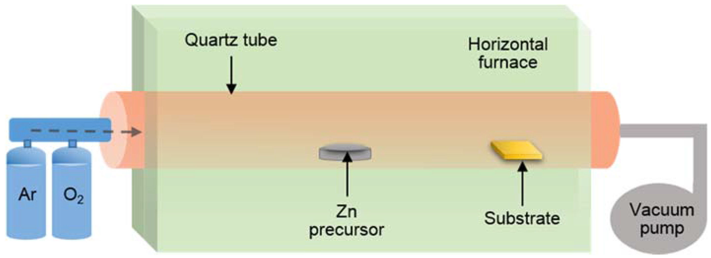
2.3. Chemical Vapor Deposition

Chemical vapor deposition (CVD) is a chemical process for the preparation of thin film nanostructures. During the deposition process, one or more volatile precursors are transported via the vapor phase to the reaction chamber where they decompose on the substrate. Heat energy is applied for activation of gas and gas–solid phase reactions. The substrate is also heated to improve the absorption of precursors (Figure 5). The morphology and the structure of the obtained material are dependent on the operating pressure of the reactor, the substrate temperature, the composition, and chemistry of the gas-phase [21]. The CVD process is carried out mainly at high temperatures (>580 °C) for fabrication of quasi-1D ZnO nanostructures [22,23]. ZnO nanorods with different diameters were obtained in the quartz tube reactor using metallic zinc as a source material. Argon and oxygen were used as the carrier and reactant [22,23]. Diethylzinc can also be used for the preparation of ZnO nanorods. Jung et al. obtained ZnO nanorods on the various types of substrates using diethylzinc as the precursor, and argon as the carrier gas. The reactor temperature was at 500 °C [24].

2.4. Atomic Layer Deposition

Atomic layer deposition (ALD) is a method based on successive, alternating surface-controlled reactions from the gas phase to produce highly conformal and uniform thin film nanostructures, and provides the thickness control at the atomic level [25,26]. The structure growth principle by ALD is similar to the CVD, except the ALD reaction breaks the CVD process into two half-reactions, keeping the precursor materials separate during the reaction. The ALD process is performed in a hot-wall horizontal flow-type reactor. The first precursor is pulsed in to the reactor and chemisorbs on the surface of the substrate. The unreacted precursor and the reaction byproducts are removed by the inert gas purge. Next, the second precursor is purged and reacts with the first precursor on the surface. At the end of the process, the unused second precursor and the reaction byproducts are also removed [25,26]. The precursors for the ALD can be solid, liquid, and gaseous. ALD is carried out at an elevated temperature for increasing the precursor and the substrate reactivity, and accelerating the sorption process [25,26,27].
ALD is a template-based technique to grow nanostructures with uniform dimensions and well-ordering. Porous anodic aluminum oxide (AAO) is a common nanotemplate for the fabrication of ZnO nanostructures by means of ALD [27,28]. Preparation of the well-ordered AAO porous arrays is an important consideration for growing uniform and highly aligned ZnO nanostructures [28]. Lim et al. grew uniform ZnO nanorod arrays on AAO porous template at 200 °C using diethyl zinc as a precursor and H2O as a reactant gas [28]. ZnO nanorods with the diameter of 60 nm (as was the diameter of AAO nanopores) were formed by filling the pores of the AAO nanotemplate. Porous AAO and diethyl zinc were also used for fabrication of well-ordered ZnO nanotube arrays [27]. The templated-assisted approach is used in order to obtain uniform and highly ordered ZnO nanostructures. However, this is the main disadvantage of ALD method; the template-assisted approach creates difficulties in the integration of existing planar structures for the development of the final device.

2.5. Physical Vapor Deposition

Physical vapor deposition (PVD) is a technique for the preparation of metal oxide nanostructures that has been optimized during recent years [29,30,31]. In this case, The ZnO nanowires can grow according to two different mechanisms: vapor-liquid-solid or vapor-solid, depending on both the source material and destination growth sites [30,31]. The PVD system consists of a tubular furnace with regulable temperature which is connected to a rotary vacuum pump in order to control the pressure inside the furnace. The substrates and the source material (powder of ZnO) are placed inside the tubular furnace. Two mass flow controllers inject the transport gases (argon or oxygen) inside the system. The powder is evaporated in the furnace at very high temperatures, in vacuum or at ambient pressure. The carrier gas is used to assist the mass transport from the evaporation region toward the substrates. In general, a catalyst (Pt, Pd, or Au, for example) is deposited on the substrates to promote the nucleation of nanostructures [30]. The morphology modifications of the fabricated nanostructures are carried out by changing the condensation temperature, the pressure inside the tubular furnace, the carrier gas flow and composition, the deposition time, and the catalyst on the target substrates. The PVD system can also be used for direct thermal oxidation of the metallic zinc to prepare ZnO nanostructures [30,31]. The thermal growth consists of two steps: metallic layer deposition and thermal oxidation. The metal oxide growth process is carried out under the oxygen flow (oxidation process); it is not a conventional PVD technique, but it may be included in this category. Thermal oxidation is the simplest among PVD processes since it may be performed in atmospheric pressure without the need of vacuum equipment.

2.6. Synthesis of Doped and FUNCTIONALIZED ZnO Nanostructures

Doping of the metal oxide materials is an effective way to improve their functional properties as well as their sensing performance [20,32]. Hydrothermal synthesis is an effective manner for the preparation of Mn- and Al-doped ZnO nanorods [33,34]. Mn has a suppression effect on the axial growth of ZnO crystals. However, Mn-doped ZnO nanorods had higher aspect ratios than un-doped ZnO. Chang et al. doped ZnO nanorods with Ce. In the first step, they prepared a ZnO seed layer on alumina substrates. Next, the samples were immersed in a solution consisting of Ce(NO3)3·6H2O, zinc nitrate hydrate, and hexamethylenetetramine [32]. In this case, it was possibnle to increase the diameter and the length of the nanorods by extending the growth time. The seed layer was applied for the preparation of titanium and aluminum doped ZnO nanorods as well [34,35]. The doping with the titanium was performed in the tubular furnace system using zinc powder and titanium wire as the precursors. To enhance the doping process the temperature of the metallic titanium precursor must be relatively high (1100–1400 °C) [35] because of its high melting point (1668 °C) [36]. During the thermal growth process, the concentration of titanium in the structure increases with the increase of the titanium precursor’s temperature. In addition, the titanium has a suspension effect on the length of nanorods (such as with Mn) [35].
The fabrication of the doped ZnO nanostructures can be also performed from the doped ZnO targets using traditional sputtering techniques, such as RF magnetron sputtering and pulsed laser deposition [37,38]. Recently the synthesis of aluminum doped ZnO nanorods by the microemulsion method with different types of surfactants was reported [39].
Functionalization of the surface of ZnO has proven to be beneficial for the improvement of its sensing properties. In recent years, ZnO quasi-1D nanostructures have been functionalized with the noble catalytic metals (Au, Pd, and Ag) mainly in the shape of nanoparticles [40,41,42]. Au is the most used catalyzer among the noble metals according to reported studies [40,43,44,45]. Au nanoparticles with uniform dispersion can be loaded using Chloroauric acid (HAuCl4) as the precursor [43,44]. Direct current (DC) sputtering is another technique for the functionalization of ZnO nanostructures with the homogeneous distribution of the Au nanoparticles [40,45]. The loading of Pd nanoparticles is performed using a solution of PdCl2 [41]. Ag functionalized ZnO nanomaterials were prepared by means of RF sputtering using mild conditions [42]. Rai et al. demonstrated the functionalization of ZnO with crystalline CuO nanoparticles (Figure 6). They performed the process using the chemical bath deposition method [46].

3. Modeling

3.1. Basic Transduction Mechanism

The sensing mechanism of metal oxides is mainly related to the population of oxygen ions (O, O2−, O 2 ) over the oxide surface, which is modulated by interaction with gaseous molecules. In particular, oxygen chemisorption is fundamental in conductometric gas sensors, since it creates acceptor surface states, which, in turn, cause an upward band-bending and the development of a surface space charge layer. In n-type oxides, such as ZnO, this is a depletion layer. The presence of such a surface barrier and its modulation due to gas-exposure determines the electrical properties of the material as well as its gas-sensing properties.
Electrical conduction in metal oxides is usually dominated by defects, both intrinsic and extrinsic. Stoichiometric oxides are usually wide band-gap semiconductors with marked ionic character [47], and thus are highly resistive. The n-type conductivity observed for most pure oxides, including ZnO, is commonly associated with oxygen vacancies, which introduces donor levels in the oxide band-gap.
The surface population of oxygen ions depends on the interplay between two kind of reactions: namely oxygen ionosorption and red/ox reactions among gaseous compounds and chemisorbed oxygen species.
The former is described through Equations (1a) and (1b), where g and ads stands for gas and adsorbed, respectively, S is an adsorption site, and e represents an electron exchanged with the semiconductor. α and β parameters assume different values depending on the form in which oxygen chemisorbs. Ionosorbed oxygen species may be either molecular (β = 2) or ionic (β = 1), and can be either singly (α = 1) or doubly ionized (α = 2). TPD, FTIR, and ESR investigations showed that below 150 °C the molecular form ( O 2 ) dominates, while above this temperature the ionic species ( O or O 2 ) dominate [48]. Lattice oxygen is typically considered not to be involved in chemiresistors due to the relatively low working temperature (below 500 °C), compared to ionic conductors.
β 2 O 2 , g + S O β , a d s
O β , a d s + α e O β , a d s α
As far as gases other than oxygen are concerned, their effect is primary distinguished based on their oxidizing or reducing character.
Oxidizing gases, such as NO2 or O3, typically interact with metallic cations withdrawing electrons from the conduction band.
Considering NO2 as an example, it oxidizes the oxide surface through different reactions, which are schematically represented by Equations (2a) and (2b) (molecular adsorption) and Equations (2c) and (2d) (dissociative adsorption):
N O 2 , g + S N O 2 , a d s
N O 2 , a d s + e N O 2 , a d s
N O 2 , g + S N O 2 , a d s
N O 2 , a d s + e N O g a s + O a d s
Usually described in terms of reduction of the oxide surface through interaction with surface oxygen species, which act as the preferred adsorption sites according to Equation (3):
C O g + O a d s C O 2 , g + e
More complex molecules, such as ethanol, can oxidize through different oxidation pathways, or can undergo different reactions from direct oxidation. Moreover, reaction by-products can further complicate the modeling of reactions occurring at sensor surfaces [47].
Once the basic equations of red-ox reactions occurring at the oxide surface are introduced, these need to be linked to the electrical properties of the semiconductor in order to explain the sensing mechanism of chemisresistor devices.
The SCL width (W) is typically calculated by solving the one-dimensional Poisson equation within the abrupt approximation (the SCL is considered completely depleted from charge carriers, outside the SCL, and the semiconductor is assumed to feature bulk properties) and by applying charge neutrality to the crystallite. This yields to a quadratic dependence of band bending on space coordinates, and W, as expressed by Equation (4), is:
W = ε r ε 0 V S q n b
where εr is the relative permittivity of the metal oxide, ε0 is the dielectric constant of vacuum, VS is the band bending, q is the electron charge, and nb is the charge carrier density.
Considering reasonable, average values for ZnO of nb ≈ 1017 cm−3 [49], εr ≈ 8 [50] and qVS ≈ 0.5 eV, [51], typical W values are of the order of several tens of nanometers.
This provides an important reference for designing effective sensitive layers: these should be nanostructured with crystallites having their size close to the space charge layer width (W). In this way, the whole semiconductor will be affected by gas-adsorption phenomena, resulting in a higher response.
In a one-dimensional geometry, the barrier height qVS, in turn, depends on the density of the surface states NS which is modulated by the aforementioned reactions with gases according to Equation (5):
q V S = q 2 N S 2 2 ε r ε 0 n b
At this level, it is worth noting that Equations (4) and (5) represent a useful, widely used, but approximated approach. Identifying the relationship between W and VS, and between qVS and NS, requires a shape dependent three-dimensional approach instead of the simplified one-dimensional approach introduced here. Solving the three dimensional Poisson equation leads to a simple equation (similar to the 1D solution reported in Equations (4) and (5)) only for the sheet morphology; cylindrical or spherical shapes require numerical solutions. Such a numerical approach has been recently reported in literature for the situation of non-completely depleted crystallites (i.e., 2W < D) showing a weak shape dependence [52]. This indicates that, even if Equations (4) and (5) are not exact, they provide a good approximation to explain the behavior of quasi-1D metal oxide nanostructures and justify their wide use in literature.
Structures typically identified as quasi-1D can be classified into two ideal situations, depending on the sensor layout and the eventual assembly of the ZnO crystallites. These will be treated separately in the following paragraphs under the approximation of Equations (4) and (5): (i) the sensing layer is composed of a single nanowire; (ii) the sensing layer is composed of an assembly of crystallites (polycrystalline structure).

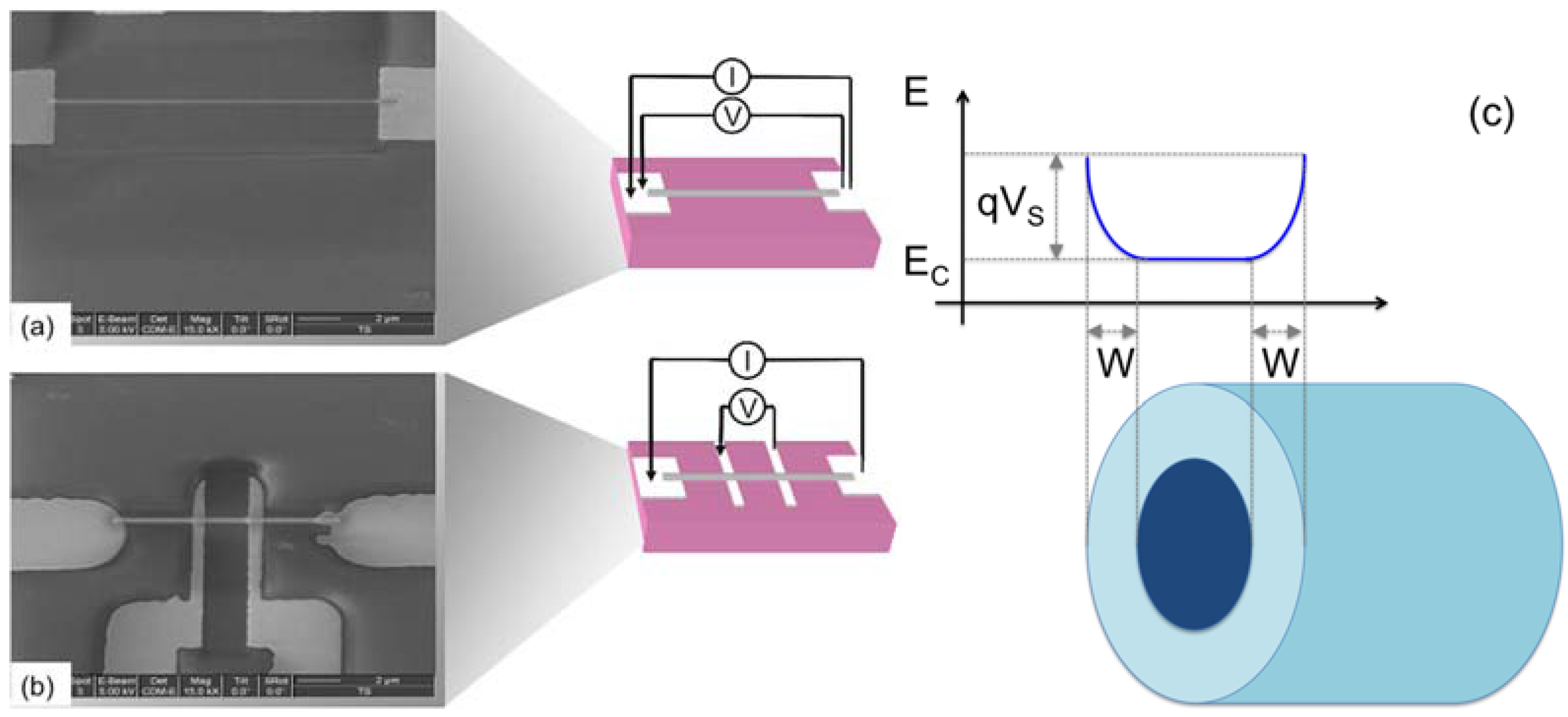
3.2. Single Nanowire Device

The single nanowire device is the simplest structure among the quasi-1D nanostructures. A single crystalline wire is used as a sensitive layer and its electrical properties are measured through two contacts (in the simplest device configuration, as shown in Figure 7a) or four contacts (Figure 7b).
Adopting the abrupt approximation, within such a device electrical conduction takes place in the inner part of the nanowire (dark colored), whose diameter is given by the difference between the nanowire geometrical diameter D and two times the SCL width (W); the situation is schematically represented in Figure 7c. The conductance of the nanowire is thus expressed by Equation (6) [53]:
G = q μ n d π ( D 2 W ) 2 4 L
where μ is the metal oxide mobility, L is the nanowire length, and W is given by Equation (4).
Equation (6) is valid until D < 2W. Considering the typical diameters of nanowires used to prepare devices, and typical W values, this works for most cases reported in the literature.
The sensor response to reducing gases is then expressed as a function of the surface bandbending by Equation (7) [53]:
S * = G g a s G a i r G a i r = 4 D ε r ε 0 q n b ( V S , a i r V S , g a s )

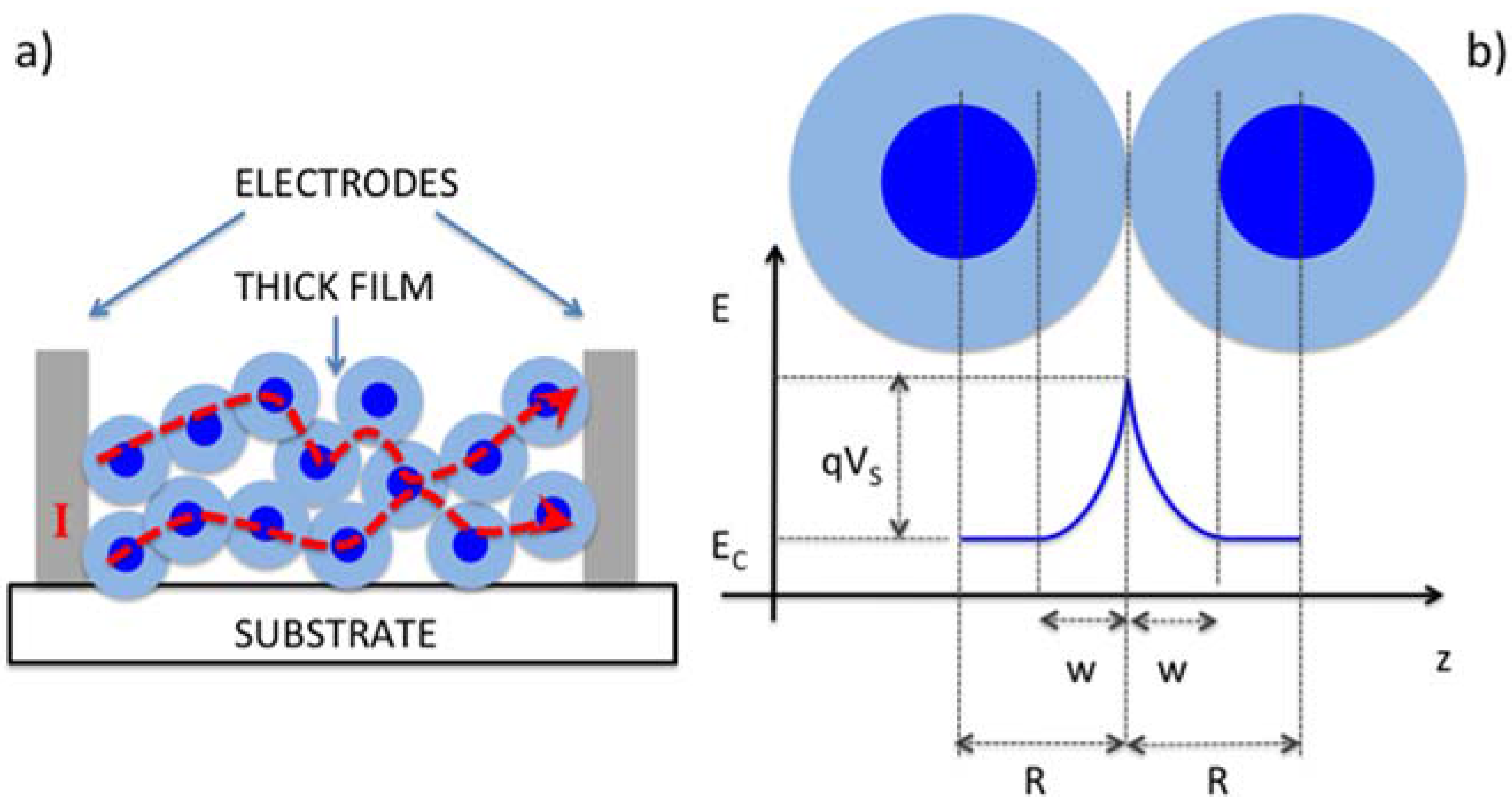
3.3. Layers with Polycrystalline Microstructure

The other ideal structure, in addition to the single nanowire, is based on polycrystalline models. This is the traditional model adopted in gas sensing, since traditional sensing layers were based either on thick of thin films, which, at the microscopic level are composed by assemblies (more or less compact) of crystallites (grains). In these structures, oxygen chemisorption occurs at the grain surface, thus raising the surface potential at grain boundaries (Figure 8). Consequently, grain boundaries are the most resistive elements in the sensing layer and dominate both electrical and sensing properties of conductometric devices. From an electrical point of view, several ZnO nanostructures are expected to behave according to such a polycrystalline model. These are, for example, nanofibers, nanotubes, or chain-shaped assemblies, which are often regarded as quasi 1D, or nanowire bundles. Considering chain assemblies, Figure 4 clearly shows the situation: besides the microscopic quasi-1D morphology, the conduction of electrons takes place from one grain to the next one, similar to what happens in polycrystalline layers. A similar situation is found in ZnO nanotubes and nanofibers, which, from a morphological/structural pint of view, are elongated assemblies of single crystalline domains. In nanowire bundles, nanowire-nanowire interfaces have been predicted to dominate the electrical and sensing properties of the device in a grain-boundary like manner.
For all these structures, the layer conductance is described by Equation (8) [51,55]:
G = G 0   exp ( q V S k T )
where the conductance G0 accounts for the layer geometry and network. In a first approximation, it does not depend either on temperature or on gas adsorption/desorption phenomena. The sensor response to a reducing gas is expressed as follows [55]:
S * = G g a s G a i r G a i r = exp ( q V S , g a s q V S , a i r k T ) 1

3.4. Surface Functionalization

The sensing mechanism of conductometric devices based on metal oxides are based on red-ox reactions modulating the surface population of oxygen ions (see Section 3.1). This means that several gases are able to induce a response in the same device, thus preventing a selective identification of a target analyte in a real atmosphere using a single gas sensor working at a constant temperature. The solution most often used to overcome this drawback is to use an array of sensors (see Section 4 for details) with different specific sensitivities. A large portion of the gas sensing field is dedicated to the development of sensors showing different sensing properties in order to address selectivity. A solution necessitates the use of sensors based on different metal oxides (ZnO, WO3, SnO2, TiO2, just to mention a few), but which also considers a given material (ZnO in this case); surface functionalization by means of nanoparticles (both metallic or in oxide forms) is an effective, catalysis-inspired approach, which has been revealed to be quite effective.
Despite the effect of catalysts on the electronic and sensing properties of ZnO, these need to be studied in detail for each catalyst and for each gas compound. A basic classification of two types of effects, namely chemical and electronic, is the worthwhile goal of this section [57].
The former is often observed with H2. H2 is activated with the catalyst and its activated fragments (H) are spilt-over to the ZnO surface for further reaction with surface oxygen species. The latter is based on the electronic properties of the catalyst-supporting oxide interface. The catalyst typically acts as an electron acceptor, thus locally decreasing the SCL at the ZnO surface. When the sensor is exposed to reducing gases, the catalyst is reduced and electrons are released back to the conduction band of the supporting ZnO.
Doping is another route to tune the properties of a given sensing layer. Typical of semiconductor technology, it uses the introduction of small amount of dopants inducing the formation of acceptor or donor states in the bulk. This will first modify the basic parameters of the material, such as the SCL width W, expressed in Equation (4), and the barrier height qVS, expressed in Equation (5). Moreover, specific sensitivity toward target compounds may be enhanced, as better detailed in Section 4.

4. Functional Properties

Several parameters, such as response and sensitivity, response and recovery times, and selectivity and stability, can be used to describe the sensing performances of chemical sensing devices. Response can be defined as the relative change in conductance or resistance for reducing or oxidizing species.
Response = (GfG0)/G0 or (RfR0)/R0
where Gf/Rf and G0/R0 are the conductance/resistance in presence of the chemical species and with the reference (air for example).
Response and recovery times may be influenced by the experimental set up, and they must be studied with great care. Sensitivity is the derivative of the response with respect to the concentration; a calibration curve with measurements at several concentrations has to be performed to get this information. Selectivity is the ability of a sensor to respond to the target species more than to other species or (better) in presence of other chemicals species, while the stability of a sensor may be measured monitoring the response over a long term operation (several weeks or months).
In order to evaluate the performances as a chemical sensor the nanostructures have to be integrated into a functional device. The integration technique adopted is strongly related to the synthesis process used to grow the nanostructures [58]. Most of the literature data are on networks of nanowires, since it is much easier and still more close to potential large-scale production compared to single nanowire devices.
In recent years, ZnO nanowires or similar morphologies have been investigated and proposed especially as hydrogen [28], acetone [9,59,60], ammonia, ethanol [11,13,14,61], hydrogen sulfide [62], nitrogen dioxide [10,13,63], and ozone [12] sensors. Nevertheless, only a few of these studies have been made considering the real working conditions of a sensor during the functional characterizations; we will report the ones we consider more interesting.
Chen et al. studied the sensing properties of flower and tube-like ZnO nanostructures, even though the gas test system is a static one, the background gas used was air; perhaps most interesting are the drift experiments that were correlated with the sensing properties [10]. An NO2 sensing mechanism was studied, and the authors found that it included electron transfer on donor sites and/or the participation of surface oxygen species to form nitrate species. Moreover, tubular ZnO had a higher ratio of donor to acceptor and more surface oxygen species than the flower-like ZnO nanostructures; this is in agreement with the better NO2 sensing performances measured in the experiments.
Sahin et al. also studied the nitrogen dioxide sensing performances of ZnO nanorods prepared on a glass substrate, the flow through technique was used with dry air as the gas carrier [64]. The interesting part of this work is that they found that the carrier transport mechanism is variable, fluctuating within the temperature interval of 303–473 K. Moreover, they investigated the effect of light activation on the sensing performances, proving that the sensing performances—in terms of response and recovery times—were enhanced, as previously reported for metal oxide thin films [65]. Under light, NO2 adsorbs on the ZnO surface, taking photogenerated electrons, and it desorbs from the surface as NO2 molecules by recombining with the photogenerated holes. The equilibrium among adsorption and desorption determine the steady-state conductance value. Furthermore, the response time may be reduced thanks to photogenerated holes. The results show this decrease, and also an almost complete recovery of the baseline conductance after the nitrogen dioxide removal, even at low temperatures, which is an interesting effect.
C. Peng at al. report about the acetone sensing performances of flower-like nanostructures, showing a good response compared to literature data, and also to commercial ZnO sensors [60]. The better performances were attributed to the better crystallinity, and the higher density of surface oxygen vacancies defects confirmed by Raman and PL studies. Furthermore, this is one of the few works in which the stability (a key parameter for real sensors) of the commercial and flower-like nanostructure is taken into consideration during the experiments. Both of the sensing devices were tested for 60 days, showing higher stability for the latter ones. Of course, longer stability tests must be performed, but at least the performances were maintained over the two months of operation.
Lately Schottky contact based sensors have been proposed in contrast with the conventional Ohmic contact sensors; these devices are promising enhanced sensitivity and improved response kinetics. In particular, ZnO micro/nano sensors for the detection of hydrogen and nitrogen dioxide at room temperature have been presented [66]. The piezotronic effect has been exploited, in addition to the Schottky contact, to develop a room temperature sensing device. Strain induced piezoelectric polarization charges enhanced the modulation of the charge carriers transport across the metal semiconductor junction thereby improving the response even at room temperature.
For further improvement in the response, selectivity, or general sensing performances of metal oxides, there are several possibilities, such as: surface modification, functionalization, or dopings/additions.
Dealing with composite metal oxides, there is an interface which is often referred to as heterojunction, and the overall structure as heterostructure. As long as there is an interface, and two different materials are in electrical contact, the Fermi levels equilibrate to the same energy resulting in charge transfer between the interface and the formation of a depletion region, causing a possible change in the sensing performances. Moreover, by having two materials exposed to chemical species there may be different reaction paths and the byproduct of the reaction with one material may react with the second material following a synergic reaction. This makes it even more difficult to understand the reaction mechanism. The improvements in sensing performances have been attributed to band bending [67], charge carrier separation [68], depletion layer modification [69,70], increased potential energy barrier [71], decreases in activation energy [72], and increased surface availability [73].
With surface modification, both response and selectivity may be modified. For example, [70] report the improvement on H2S performances by depositing an ultrathin layer of copper oxide on the zinc oxide nanowires surface. CuO is well known for reacting with H2S to form CuS. CuS has a metallic behavior and causes a huge change in the resistivity of the active material. Furthermore, the effects of CuO nanoparticles on ZnO nanorods have also been reported for carbon monoxide sensing in [46] showing both a decrease in the overall resistance and an increase in the response (Figure 10). This enhancement was attributed to an increase of the electron-hole pairs lifetime of CuO/ZnO nanorods that facilitates the absorption of gas molecules, and by the preferential absorption of CO through Cu-CO bonding.
The use of surface modification has also been proposed for the detection of nitrogen dioxide and ethanol; ZnO nanowires were decorated with Co3O4 particles [74] and showed an increase in the resistance due to the extension of the electron depletion layer by the formation of p-n junctions between cobalt and zinc oxide. Due to this, and to the catalytic effect of nanocrystalline Co3O4 particles, the sensors were able to increase their selectivity towards nitrogen dioxide and ethanol.
Cr2O3 was also used on ZnO nanowires for the formation of p–n junction heterostructures and tested in the presence of tri-methylamine [75]; the results showed an enhancement in the response for the decoration with nanoparticles, while the core shell heterostructure decreased the response compared to ZnO nanowires (Figure 9). The authors ascribed this behavior to the catalytic effect of Cr2O3 nanoparticles and the extension of the electron depletion layer. It was also shown that the dominant conduction path through the p-type Cr2O3 layer in the core shell nanostructures showed p-type behavior.
Moreover, recent studies show that the functionalization of ZnO with graphene-based materials is a promising approach for the enhancement of its sensing performance; reducing the graphene oxide layers by varying the preparation conditions is an especially suitable way to realize the functionalization of ZnO [76,77,78,79]. Graphene oxide/ZnO composite structures are tested mostly near room temperatures [80,81,82], because at high temperatures they can be chemically reduced [80]. The modification of the surface structure of the ZnO by the graphene/graphene oxide significantly reduces the optimum working temperature and increases its sensing performances towards hydrogen, ammonia, ethanol, and oxygen [76,77,79,83,84].
All these works report new ways in which functionalization and heterostructures may change the gas sensing performances, and propose complex configurations, thereby unfortunately adding or increasing new/existing challenges. For example, thermal and electrical stability over long-term operation may become even more challenging than for bare oxide structures. Reproducibility in sensing performances, which is essential for a real application as commercial sensing devices in a large-scale production, becomes even more difficult when we are dealing with composite materials. The same holds for understanding the working mechanisms. Therefore, a great amount of attention must be used when dealing with these structures, studying not only the individual sensing performances, but all these other parameters that have until now prevented their use in commercial sensing devices. In Table 1 we summarized the sensing performance of conductometric chemical sensors based on pure, doped, and functionalized quasi-1D ZnO nanostructures prepared with the different methods.
Finally, very recently the chemical sensors based on quasi-1D ZnO nanostructures have been studied for applications in food quality monitoring [85]. Among the different sensory characteristics, the most important parameter for the food quality monitoring is the aroma (finger-print) [86]. It may offer information about the safety and quality of the food, acting sometimes as an indicator of processing mistakes as well. Electronic nose (EN) is a device for aroma profile analysis. EN consists of an array of gas sensors with different selectivities, a signal collecting unit, and pattern recognition software [86]. EN is applied to determine the quality of many products such as: oil, extra virgin olive oil, milk, tomato-based products, coffee, cheeses, fresh meat, juices, fruit, etc. [86,87]. Quasi-1D ZnO nanostructures with their good sensitivity toward acetone and ethanol may open an entirely new era in the development of the innovative metal oxide gas sensors [85,87].

5. Conclusions

In this review, we summarized the recent advances in the synthesis of the quasi-1D ZnO nanostructures for potential applications in conductometric gas sensors fabrication. The growth mechanism of ZnO nanostructures mainly involves chemical or physical reactions, nucleation, and conversion into the assemblies using the direct chemical and physical deposition techniques. The preparation methods are based on two main growth process: bottom-up and top-down, including catalyst-free and catalyst-assisted fabrication procedures. The hydrothermal synthesis, ALD, CVD, and PVD growth procedures usually performed using catalyst or template layers, consequently allow for the controlling of the shape and the dimensions of the structure. The main disadvantage of these methods is that the presence of other materials as catalytic or template layers may interfere with their integration in existing planar structures for the final device fabrication. In addition, both the hydrothermal process and thermal oxidation are carried out at relatively high temperatures thereby limiting the substrate choice, because the high temperature processes may damage the temperature-sensitive substrates. The electrochemical anodization method allows for the tailoring of the structure shape and dimensions at room temperature by variation of the anodization parameters. It is a low-cost and easy method for fabrication of quasi-1D structures, with the disadvantage of a poor crystallinity of the materials grown at room temperature.
When these nanostructures are exploited as conductometric sensors, the interplay between morphological, structural, and electrical properties should be considered in order to identify the right transduction mechanism. From an electrical point of view, single crystalline domains are the most conductive units, so if interfaces are present among these domains, interfaces will be the dominant elements concerning electrical properties, and thus sensing performance of chemiresistors. This will determine the proper transducing framework (whether quasi-1D or polycrystalline) for the different structures typically described as quasi-1D based on pure morphological arguments.
In the recent literature, most of the reports are on nanowires networks, with increasing attention to obtain reproducible data and studying real working condition for prototype sensing devices. Studies on the sensing performances drift and “operando” spectroscopies are attracting more attention thereby helping with understanding and mastering of sensing properties. Moreover, new sensing mechanisms have been proposed, such as Schottky contact based sensors integrated with the exploitation of peculiar piezotronic properties of ZnO.
However, solving the problems related to the selectivity and sensitivity of ZnO in gas sensing applications still remains a major challenge. The different sensing behaviors reported for doped and functionalized ZnO nanostructures toward different gases and vapors are encouraging, and together with the use of electronic noses will reduce the problem of the selectivity.
With the accurate control of the structure dimensions and composition, and a critical understanding of the modified properties of the material, progress will be made, and consequently new and interesting quasi-1D nanomaterials will create the sensing technologies of the future.

Acknowledgments

The research leading to these results has received funding from the following projects: “New approaches and methodologies for bioremediation of water contaminated by chlorinated aliphatic solvents (SUSBIOREM)” (funded by the National Research Council (CNR) and Lombardia Region); “MSP: Multi Sensor Platform for Smart Building Management” (grant agreement No. 611887, funded by the European Commission through its 7th Framework Programme); “FIRB—Oxides at the nanoscale: multifunctionality and applications” (Protocollo: RBAP115AYN, funded by the Italian Ministry of Education); “ORAMA” (grant agreement NMP3-LA-2010-246334, funded by the European Commission through its 7th Framework Programme); “WIROX: Oxide Nanostructures for Wireless Chemical Sensing” (PEOPLE MARIE CURIE ACTIONS, International Research Staff Exchange Scheme, Call: FP7-PEOPLE-2011-IRSES, 2012–2015). The authors also thank the scientists cited in this review paper for their contributions to the research.

Conflicts of Interest

The authors declare no conflict of interest.

References

  1. Comini, E.; Baratto, C.; Faglia, G.; Ferroni, M.; Vomiero, A.; Sberveglieri, G. Quasi-one dimensional metal oxide semiconductors: Preparation, characterization and application as chemical sensors. Prog. Mater. Sci. 2009, 54, 1–67. [Google Scholar] [CrossRef]
  2. Yuan, Q.; Zhao, Y.-P.; Li, L.; Wang, T. Ab initio study of ZnO-based gas-sensing mechanisms: Surface reconstruction and charge transfer. J. Phys. Chem. C 2009, 113, 6107–6113. [Google Scholar] [CrossRef]
  3. Morin, F.J. Semiconductors; Renhold Publishing Company: New York, NY, USA, 1959. [Google Scholar]
  4. Morkoç, H.; Özgür, Ü. General Properties of ZnO, in Zinc Oxide: Fundamentals, Materials and Device Technology; Wiley-VCH Verlag GmbH & Co. KGaA: Weinheim, Germany, 2009; p. 76. [Google Scholar]
  5. Spencer, M.J.S. Gas sensing applications of 1d-nanostructured zinc oxide: Insights from density functional theory calculations. Prog. Mater. Sci. 2012, 57, 437–486. [Google Scholar] [CrossRef]
  6. Yu, A.; Jiang, P.; Wang, Z.L. Nanogenerator as self-powered vibration sensor. Nano Energy 2012, 1, 418–423. [Google Scholar] [CrossRef]
  7. Hu, J.T.; Odom, T.W.; Lieber, C.M. Chemistry and physics in one dimension: Synthesis and properties of nanowires and nanotubes. Acc. Chem. Res. 1999, 32, 435–445. [Google Scholar] [CrossRef]
  8. Guo, W.; Liu, T.; Huang, L.; Zhang, H.; Zhou, Q.; Zeng, W. Hmt assisted hydrothermal synthesis of various ZnO nanostructures: Structure, growth and gas sensor properties. Phys. E-Low-Dimens. Syst. Nanostruct. 2011, 44, 680–685. [Google Scholar] [CrossRef]
  9. Song, H.; Yang, H.; Ma, X. A comparative study of porous ZnO nanostructures synthesized from different zinc salts as gas sensor materials. J. Alloys Compd. 2013, 578, 272–278. [Google Scholar] [CrossRef]
  10. Chen, M.; Wang, Z.; Han, D.; Gu, F.; Guo, G. High-sensitivity NO2 gas sensors based on flower-like and tube-like ZnO nanomaterials. Sens. Actuators B Chem. 2011, 157, 565–574. [Google Scholar] [CrossRef]
  11. Wang, L.; Kang, Y.; Liu, X.; Zhang, S.; Huang, W.; Wang, S. ZnO nanorod gas sensor for ethanol detection. Sens. Actuators B Chem. 2012, 162, 237–243. [Google Scholar] [CrossRef]
  12. Catto, A.C.; da Silva, L.F.; Ribeiro, C.; Bernardini, S.; Aguir, K.; Longo, E.; Mastelaro, V.R. An easy method of preparing ozone gas sensors based on ZnO nanorods. RSC Adv. 2015, 5, 19528–19533. [Google Scholar] [CrossRef]
  13. Rai, P.; Raj, S.; Ko, K.-J.; Park, K.-K.; Yu, Y.-T. Synthesis of flower-like ZnO microstructures for gas sensor applications. Sens. Actuators B Chem. 2013, 178, 107–112. [Google Scholar] [CrossRef]
  14. Yin, M.; Liu, M.; Liu, S. Diameter regulated ZnO nanorod synthesis and its application in gas sensor optimization. J. Alloys Compd. 2014, 586, 436–440. [Google Scholar] [CrossRef]
  15. Shrestha, N.K.; Lee, K.; Hahn, R.; Schmuki, P. Anodic growth of hierarchically structured nanotubular ZnO architectures on zinc surfaces using a sulfide based electrolyte. Electrochem. Commun. 2013, 34, 9–13. [Google Scholar] [CrossRef]
  16. Park, J.; Kim, K.; Choi, J. Formation of ZnO nanowires during short durations of potentiostatic and galvanostatic anodization. Curr. Appl. Phys. 2013, 13, 1370–1375. [Google Scholar] [CrossRef]
  17. Galstyan, V.; Comini, E.; Baratto, C.; Ponzoni, A.; Bontempi, E.; Brisotto, M.; Faglia, G.; Sberveglieri, G. Synthesis of self-assembled chain-like ZnO nanostructures on stiff and flexible substrates. CrystEngComm 2013, 15, 2881–2887. [Google Scholar] [CrossRef]
  18. Hu, Z.; Chen, Q.; Li, Z.; Yu, Y.; Peng, L.-M. Large-scale and rapid synthesis of ultralong ZnO nanowire films via anodization. J. Phys. Chem. C 2010, 114, 881–889. [Google Scholar] [CrossRef]
  19. Galstyan, V.; Comini, E.; Baratto, C.; Faglia, G.; Sberveglieri, G. Nanostructured zno chemical gas sensors. Ceram. Int. 2015, 41, 14239–14244. [Google Scholar] [CrossRef]
  20. Galstyan, V.; Comini, E.; Faglia, G.; Sberveglieri, G. TiO2 nanotubes: Recent advances in synthesis and gas sensing properties. Sensors 2013, 13, 14813–14838. [Google Scholar] [CrossRef] [PubMed]
  21. Jones, A.C.; Hitchman, M.L. Overview of chemical vapour deposition. Chem. Vap. Depos. Precursors Process. Appl. 2008, Chapter 1. 1–36. [Google Scholar]
  22. Al-Salman, H.S.; Abdullah, M.J. Rf sputtering enhanced the morphology and photoluminescence of multi-oriented ZnO nanostructure produced by chemical vapor deposition. J. Alloys Compd. 2013, 547, 132–137. [Google Scholar] [CrossRef]
  23. Chien, F.S.-S.; Wang, C.-R.; Chan, Y.-L.; Lin, H.-L.; Chen, M.-H.; Wu, R.-J. Fast-response ozone sensor with ZnO nanorods grown by chemical vapor deposition. Sensors Actuators B Chem. 2010, 144, 120–125. [Google Scholar] [CrossRef]
  24. Jung, I.O.; Park, J.Y.; Kim, S.S. Substrate dependent growth modes of ZnO nanorods grown by metalorganic chemical vapor deposition. J. Cryst. Growth 2012, 355, 78–83. [Google Scholar] [CrossRef]
  25. Devi, A. Old chemistries’ for new applications: Perspectives for development of precursors for MOCVD and ALD applications. Coord. Chem. Rev. 2013, 257, 3332–3384. [Google Scholar] [CrossRef]
  26. Emslie, D.J.H.; Chadha, P.; Price, J.S. Metal ald and pulsed CVD: Fundamental reactions and links with solution chemistry. Coord. Chem. Rev. 2013, 257, 3282–3296. [Google Scholar] [CrossRef]
  27. Zhang, Y.; Liu, M.; Ren, W.; Ye, Z.-G. Well-ordered ZnO nanotube arrays and networks grown by atomic layer deposition. Appl. Surf. Sci. 2015, 340, 120–125. [Google Scholar] [CrossRef]
  28. Lim, Y.T.; Son, J.Y.; Rhee, J.S. Vertical ZnO nanorod array as an effective hydrogen gas sensor. Ceram. Int. 2013, 39, 887–890. [Google Scholar] [CrossRef]
  29. Comini, E. One- and two-dimensional metal oxide nanostructures for chemical sensing. In Semiconductor Gas Sensors; Jaaniso, R., Tan, O.K., Eds.; Woodhead Publishing Limited: Sawston, Cambridge, UK, 2013; pp. 299–315. [Google Scholar]
  30. Comini, E.; Baratto, C.; Concina, I.; Faglia, G.; Falasconi, M.; Ferroni, M.; Galstyan, V.; Gobbi, E.; Ponzoni, A.; Vomiero, A.; et al. Metal oxide nanoscience and nanotechnology for chemical sensors. Sens. Actuators B Chem. 2013, 179, 3–20. [Google Scholar] [CrossRef]
  31. Jimenez-Cadena, G.; Comini, E.; Ferroni, M.; Vomiero, A.; Sberveglieri, G. Synthesis of different ZnO nanostructures by modified PVD process and potential use for 1dye-sensitized solar cells. Mater. Chem. Phys. 2010, 124, 694–698. [Google Scholar] [CrossRef]
  32. Chang, C.-J.; Lin, C.-Y.; Chen, J.-K.; Hsu, M.-H. Ce-doped ZnO nanorods based low operation temperature NO2 gas sensors. Ceram. Int. 2014, 40, 10867–10875. [Google Scholar] [CrossRef]
  33. Ahmed, F.; Arshi, N.; Anwar, M.S.; Danish, R.; Koo, B.H. Mn-doped ZnO nanorod gas sensor for oxygen detection. Curr. Appl. Phys. 2013, 13, S64–S68. [Google Scholar] [CrossRef]
  34. Zhou, H.; Mei, J.; Gui, P.; Tao, P.; Song, Z.; Wang, H.; Fang, G.-J. The investigation of Al-doped ZnO as an electron transporting layer for visible-blind ultraviolet photodetector based on n-ZnO nanorods/p-si heterojunction. Mater. Sci. Semiconduct. Process. 2015, 38, 67–71. [Google Scholar] [CrossRef]
  35. Hsu, C.-L.; Gao, Y.-D.; Chen, Y.-S.; Hsueh, T.-J. Vertical Ti doped ZnO nanorods based on ethanol gas sensor prepared on glass by furnace system with hotwire assistance. Sens. Actuators B Chem. 2014, 192, 550–557. [Google Scholar] [CrossRef]
  36. Macdonald, F.; Lide, D.R. CRC handbook of chemistry and physics: From paper to web. Abstr. Pap. Am. Chem. Soc. 2003, 225, U552. [Google Scholar]
  37. Jeong, D.; Kim, K.; Park, S.-I.; Kim, Y.-H.; Kim, S.; Kim, S.-I. Characteristics of Ga and Ag-doped ZnO-based nanowires for an ethanol gas sensor prepared by hot-walled pulsed laser deposition. Res. Chem. Intermed. 2014, 40, 97–103. [Google Scholar] [CrossRef]
  38. Liu, Y.; Zhou, W.; Huang, Y.; Wu, P. Unexpected ferromagnetism in n-type polycrystalline K-doped ZnO films prepared by RF-magnetron sputtering. J. Mater. Sci. Mater. Electron. 2015, 26, 8451–8455. [Google Scholar] [CrossRef]
  39. Lim, S.K.; Hong, S.H.; Hwang, S.-H.; Choi, W.M.; Kim, S.; Park, H.; Jeong, M.G. Synthesis of Al-doped ZnO nanorods via microemulsion method and their application as a CO gas sensor. J. Mater. Sci. Technol. 2015, 31, 639–644. [Google Scholar] [CrossRef]
  40. Hosseini, Z.S.; Mortezaali, A.; Zad, A.I.; Fardindoost, S. Sensitive and selective room temperature H2S gas sensor based on Au sensitized vertical ZnO nanorods with flower-like structures. J. Alloys Compd. 2015, 628, 222–229. [Google Scholar] [CrossRef]
  41. Singh, P.; Singh, V.N.; Jain, K.; Senguttuvan, T.D. Pulse-like highly selective gas sensors based on ZnO nanostructures synthesized by a chemical route; effect of In doping and Pd loading. Sens. Actuators B Chem. 2012, 166. [Google Scholar] [CrossRef]
  42. Simon, Q.; Barreca, D.; Gasparotto, A.; Maccato, C.; Tondello, E.; Sada, C.; Comini, E.; Devi, A.; Fischer, R.A. Ag/ZnO nanomaterials as high performance sensors for flammable and toxic gases. Nanotechnology 2012, 23, 025502. [Google Scholar] [CrossRef] [PubMed]
  43. Guo, J.; Zhang, J.; Zhu, M.; Ju, D.; Xu, H.; Cao, B. High-performance gas sensor based on ZnO nanowires functionalized by au nanoparticles. Sens. Actuators B Chem. 2014, 199, 339–345. [Google Scholar] [CrossRef]
  44. Wang, L.; Wang, S.; Xu, M.; Hu, X.; Zhang, H.; Wang, Y.; Huang, W. A Au-functionalized ZnO nanowire gas sensor for detection of benzene and toluene. Phys. Chem. Chem. Phys. 2013, 15, 17179–17186. [Google Scholar] [CrossRef] [PubMed]
  45. Mun, Y.; Park, S.; An, S.; Lee, C.; Kim, H.W. NO2 gas sensing properties of Au-functionalized porous ZnO nanosheets enhanced by UV irradiation. Ceram. Int. 2013, 39, 8615–8622. [Google Scholar] [CrossRef]
  46. Rai, P.; Jeon, S.-H.; Lee, C.-H.; Lee, J.-H.; Yu, Y.-T. Functionalization of ZnO nanorods by CuO nanospikes for gas sensor applications. RSC Adv. 2014, 4, 23604–23609. [Google Scholar] [CrossRef]
  47. Henrich, V.E.; Cox, P.A. The Surface Science of Metal Oxides; Cambridge University Press: Cambridge, UK, 1994; p. 464. [Google Scholar]
  48. Barsan, N.; Weimar, U. Conduction model of metal oxide gas sensors. J. Electroceram. 2001, 7, 143–167. [Google Scholar] [CrossRef]
  49. Yun, Y.S.; Park, J.Y.; Oh, H.; Kim, J.J.; Kim, S.S. Electrical transport properties of size-tuned ZnO nanorods. J. Mater. Res. 2006, 21, 132–136. [Google Scholar] [CrossRef]
  50. Ozgur, U.; Alivov, Y.I.; Liu, C.; Teke, A.; Reshchikov, M.A.; Dogan, S.; Avrutin, V.; Cho, S.J.; Morkoc, H. A comprehensive review of ZnO materials and devices. J. Appl. Phys. 2005, 98, 041301. [Google Scholar] [CrossRef]
  51. Lantto, V.; Rompplainen, P.; Leppävuori, S. A study of the temperature dependence of the barrier energy in porous tin dioxide. Sensors Actuators 1988, 14, 149–163. [Google Scholar] [CrossRef]
  52. Rebholz, J.; Bonanati, P.; Weimar, U.; Barsan, N. Grain shape influence on semiconducting metal oxide based gas sensor performance: Modeling versus experiment. Anal. Bioanal. Chem. 2014, 406, 3977–3983. [Google Scholar] [CrossRef] [PubMed]
  53. Chen, P.-C.; Shen, G.; Zhou, C. Chemical sensors and electronic noses based on 1-D metal oxide nanostructures. IEEE Trans. Nanotechnol. 2008, 7, 668–682. [Google Scholar] [CrossRef]
  54. Schwamb, T.; Burg, B.R.; Schirmer, N.C.; Poulikakos, D. On the effect of the electrical contact resistance in nanodevices. Appl. Phys. Lett. 2008, 92, 243106. [Google Scholar] [CrossRef]
  55. Sysoev, V.V.; Goschnick, J.; Schneider, T.; Strelcov, E.; Kolmakov, A. A gradient microarray electronic nose based on percolating SnO2 nanowire sensing elements. Nano Lett. 2007, 7, 3182–3188. [Google Scholar] [CrossRef] [PubMed]
  56. Ponzoni, A.; Comini, E.; Concina, I.; Ferroni, M.; Falasconi, M.; Gobbi, E.; Sberveglieri, V.; Sberveglieri, G. Nanostructured metal oxide gas sensors, a survey of applications carried out at sensor lab, Brescia (Italy) in the security and food quality fields. Sensors 2012, 12, 17023–17045. [Google Scholar] [CrossRef] [PubMed] [Green Version]
  57. Yamazoe, N.; Sakai, G.; Shimanoe, K. Oxide semiconductor gas sensors. Catal. Surv. Asia 2003, 7, 63–75. [Google Scholar] [CrossRef]
  58. Comini, E.; Baratto, C.; Faglia, G.; Ferroni, M.; Ponzoni, A.; Zappa, D.; Sberveglieri, G. Metal oxide nanowire chemical and biochemical sensors. J. Mater. Res. 2013, 28, 2911–2931. [Google Scholar] [CrossRef]
  59. Pawar, R.C.; Shaikh, J.S.; Suryavanshi, S.S.; Patil, P.S. Growth of ZnO nanodisk, nanospindles and nanoflowers for gas sensor: PH dependency. Curr. Appl. Phys. 2012, 12, 778–783. [Google Scholar] [CrossRef]
  60. Peng, C.; Guo, J.; Yang, W.; Shi, C.; Liu, M.; Zheng, Y.; Xu, J.; Chen, P.; Huang, T.; Yang, Y. Synthesis of three-dimensional flower-like hierarchical ZnO nanostructure and its enhanced acetone gas sensing properties. J. Alloys Compd. 2016, 654, 371–378. [Google Scholar] [CrossRef]
  61. Zou, A.L.; Hu, L.Z.; Qiu, Y.; Cao, G.Y.; Yu, J.J.; Wang, L.N.; Zhang, H.Q.; Yin, B.; Xu, L.L. High performance of 1-D ZnO microwire with curve-side hexagon as ethanol gas sensor. J. Mater. Sci. Mater. Electron. 2015, 26, 4908–4912. [Google Scholar] [CrossRef]
  62. Shinde, S.D.; Patil, G.E.; Kajale, D.D.; Gaikwad, V.B.; Jain, G.H. Synthesis of ZnO nanorods by spray pyrolysis for H2S gas sensor. J. Alloys Compd. 2012, 528, 109–114. [Google Scholar] [CrossRef]
  63. .Kumar, R.; Al-Dossary, O.; Kumar, G.; Umar, A. Zinc oxide nanostructures for NO2 gas-sensor applications: A review. Nano-Micro Lett. 2015, 7, 97–120. [Google Scholar] [CrossRef]
  64. Sahin, Y.; Ozturk, S.; Kilinc, N.; Kosemen, A.; Erkovan, M.; Ozturk, Z.Z. Electrical conduction and NO2 gas sensing properties of ZnO nanorods. Appl. Surf. Sci. 2014, 303, 90–96. [Google Scholar] [CrossRef]
  65. Comini, E.; Faglia, G.; Sberveglieri, G. UV light activation of tin oxide thin films for NO2 sensing at low temperatures. Sensors Actuators B Chem. 2001, 78, 73–77. [Google Scholar] [CrossRef]
  66. Zhou, R.; Hu, G.; Yu, R.; Pan, C.; Wang, Z.L. Piezotronic effect enhanced detection of flammable/toxic gases by ZnO micro/nanowire sensors. Nano Energy 2015, 12, 588–596. [Google Scholar] [CrossRef]
  67. Kusior, A.; Radecka, M.; Rekas, M.; Lubecka, M.; Zakrzewska, K.; Reszka, A.; Kowalski, B.J. Sensitization of gas sensing properties in TiO2/SnO2 nanocomposites. Procedia Eng. 2012, 47, 1073–1076. [Google Scholar] [CrossRef]
  68. Yu, X.; Zhang, G.; Cao, H.; An, X.; Wang, Y.; Shu, Z.; An, X.; Hua, F. ZnO@ZnS hollow dumbbells-graphene composites as high-performance photocatalysts and alcohol sensors. New J. Chem. 2012, 36, 2593–2598. [Google Scholar] [CrossRef]
  69. Liu, Y.; Zhu, G.; Chen, J.; Xu, H.; Shen, X.; Yuan, A. Co3O4/ZnO nanocomposites for gas-sensing applications. Appl. Surf. Sci. 2013, 265, 379–384. [Google Scholar] [CrossRef]
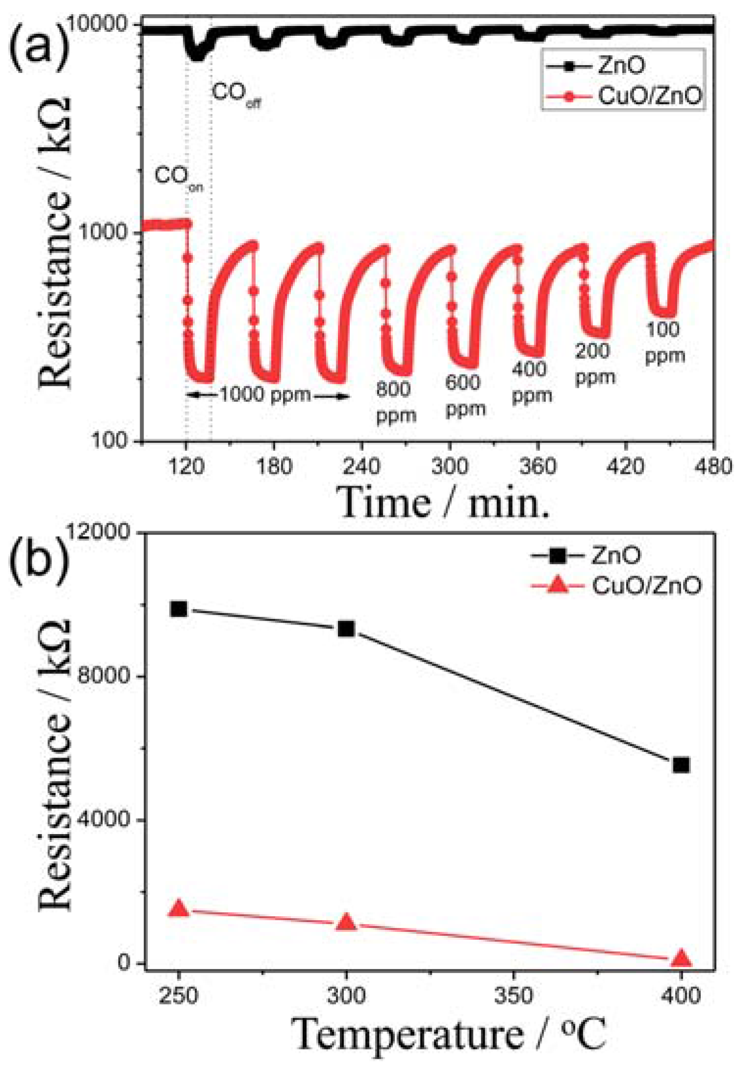
  70. Wang, L.; Kang, Y.; Wang, Y.; Zhu, B.; Zhang, S.; Huang, W.; Wang, S. CuO nanoparticle decorated ZnO nanorod sensor for low-temperature H2S detection. Mater. Sci. Eng. C Mater. Biol. Appl. 2012, 32, 2079–2085. [Google Scholar] [CrossRef]
  71. Wang, W.; Li, Z.; Zheng, W.; Huang, H.; Wang, C.; Sun, J. Cr2O3-sensitized ZnO electrospun nanofibers based ethanol detectors. Sens. Actuators B Chem. 2010, 143, 754–758. [Google Scholar] [CrossRef]
  72. Gu, H.; Wang, Z.; Hu, Y. Hydrogen gas sensors based on semiconductor oxide nanostructures. Sensors 2012, 12, 5517–5550. [Google Scholar] [CrossRef] [PubMed]
  73. Zeng, Y.; Bing, Y.-F.; Liu, C.; Zheng, W.-T.; Zou, G.-T. Self-assembly of hierarchical ZnSnO3-SnO2 nanoflakes and their gas sensing properties. Trans. Nonferr. Metals Soc. China 2012, 22, 2451–2458. [Google Scholar] [CrossRef]
  74. Na, C.W.; Woo, H.-S.; Kim, I.-D.; Lee, J.-H. Selective detection of NO2 and C2H5OH using a Co3O4-decorated ZnO nanowire network sensor. Chem. Commun. 2011, 47, 5148–5150. [Google Scholar] [CrossRef] [PubMed]
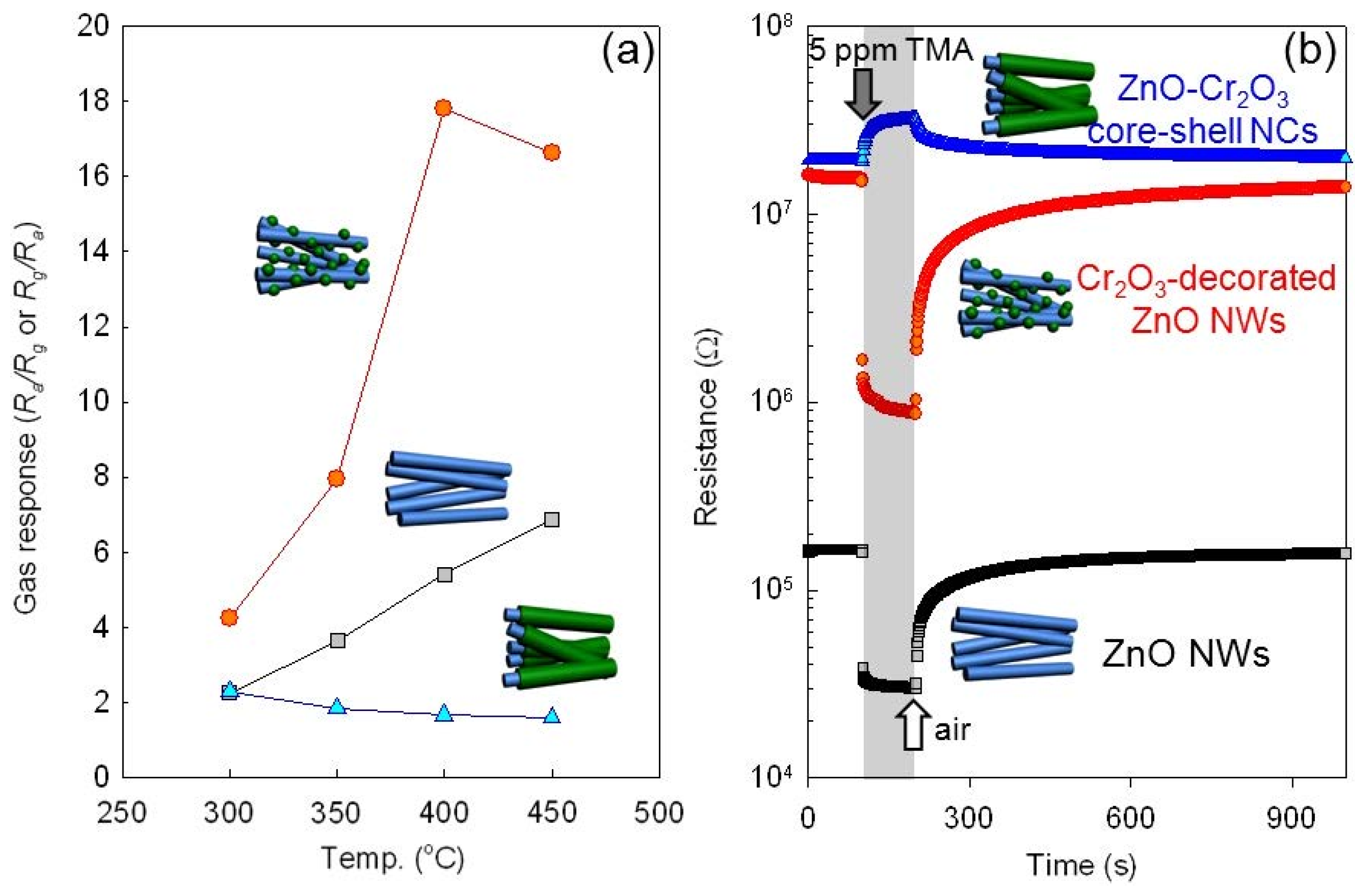
  75. Woo, H.-S.; Na, C.; Kim, I.-D.; Lee, J.-H. Highly sensitive and selective trimethylamine sensor using one-dimensional ZnO-Cr2O3 hetero-nanostructures. Nanotechnology 2012, 23, 245501. [Google Scholar] [CrossRef] [PubMed]
  76. Song, N.; Fan, H.; Tian, H. PVP assisted in situ synthesis of functionalized graphene/ZnO (FGZnO) nanohybrids with enhanced gas-sensing property. J. Mater. Sci. 2015, 50, 2229–2238. [Google Scholar] [CrossRef]
  77. Khadem, S.M.J.; Abdi, Y.; Darbari, S.; Ostovari, F. Investigating the effect of gas absorption on the electromechanical and electrochemical behavior of graphene/ZnO structure, suitable for highly selective and sensitive gas sensors. Curr. Appl. Phys. 2014, 14, 1498–1503. [Google Scholar] [CrossRef]
  78. Zhou, Y.; Xie, G.; Xie, T.; Yuan, H.; Tai, H.; Jiang, Y.; Chen, Z. A sensitive film structure improvement of reduced graphene oxide based resistive gas sensors. Appl. Phys. Lett. 2014, 105, 033502. [Google Scholar] [CrossRef]
  79. Afzali, P.; Abdi, Y.; Arzi, E. Directional reduction of graphene oxide sheets using photocatalytic activity of ZnO nanowires for the fabrication of a high sensitive oxygen sensor. Sens. Actuators B Chem. 2014, 195, 92–97. [Google Scholar] [CrossRef]
  80. Toda, K.; Furue, R.; Hayami, S. Recent progress in applications of graphene oxide for gas sensing: A review. Anal. Chim. Acta 2015, 878, 43–53. [Google Scholar] [CrossRef] [PubMed]
  81. Zhou, Y.; Jiang, Y.; Xie, T.; Tai, H.; Xie, G. A novel sensing mechanism for resistive gas sensors based on layered reduced graphene oxide thin films at room temperature. Sens. Actuators B Chem. 2014, 203, 135–142. [Google Scholar] [CrossRef]
  82. Hu, N.; Yang, Z.; Wang, Y.; Zhang, L.; Wang, Y.; Huang, X.; Wei, H.; Wei, L.; Zhang, Y. Ultrafast and sensitive room temperature NH3 gas sensors based on chemically reduced graphene oxide. Nanotechnology 2014, 25, 025502. [Google Scholar] [CrossRef] [PubMed]
  83. Yi, J.; Lee, J.M.; Il Park, W. Vertically aligned ZnO nanorods and graphene hybrid architectures for high-sensitive flexible gas sensors. Sens. Actuators B Chem. 2011, 155, 264–269. [Google Scholar] [CrossRef]
  84. Anand, K.; Singh, O.; Singh, M.P.; Kaur, J.; Singh, R.C. Hydrogen sensor based on graphene/ZnO nanocomposite. Sens. Actuators B Chem. 2014, 195, 409–415. [Google Scholar] [CrossRef]
  85. Nesakumar, N.; Sethuraman, S.; Krishnan, U.M.; Rayappan, J.B.B. Chemometric methods for the evaluation of electron transfer properties of zinc oxide nanorods modified gold electrode for lactate detection in food products. J. Comput. Theor. Nanosci. 2015, 12, 407–412. [Google Scholar] [CrossRef]
  86. Peris, M.; Escuder-Gilabert, L. A 21st century technique for food control: Electronic noses. Anal. Chim. Acta 2009, 638, 1–15. [Google Scholar] [CrossRef] [PubMed]
  87. Concina, I.; Falasconi, M.; Sberveglieri, V. Electronic noses as flexible tools to assess food quality and safety: Should we trust them? IEEE Sensors J. 2012, 12, 3232–3237. [Google Scholar] [CrossRef]
  88. Lupan, O.; Ursaki, V.V.; Chai, G.; Chow, L.; Emelchenko, G.A.; Tiginyanu, I.M.; Gruzintsev, A.N.; Redkin, A.N. Selective hydrogen gas nanosensor using individual ZnO nanowire with fast response at room temperature. Sens. Actuators B Chem. 2010, 144, 56–66. [Google Scholar] [CrossRef]
  89. Cardoza-Contreras, M.N.; Romo-Herrera, J.M.; Rios, L.A.; Garcia-Gutierrez, R.; Zepeda, T.A.; Contreras, O.E. Single ZnO nanowire-based gas sensors to detect low concentrations of hydrogen. Sensors 2015, 15, 30539–30544. [Google Scholar] [CrossRef] [PubMed]
  90. Shao, C.; Chang, Y.; Long, Y. High performance of nanostructured ZnO film gas sensor at room temperature. Sens. Actuators B Chem. 2014, 204, 666–672. [Google Scholar] [CrossRef]
  91. Chen, T.-Y.; Chen, H.-I.; Hsu, C.-S.; Huang, C.-C.; Wu, J.-S.; Chou, P.-C.; Liu, W.-C. Characteristics of ZnO nanorods-based ammonia gas sensors with a cross-linked configuration. Sens. Actuators B Chem. 2015, 221, 491–498. [Google Scholar] [CrossRef]
  92. Gu, C.; Li, S.; Huang, J.; Shi, C.; Liu, J. Preferential growth of long ZnO nanowires and its application in gas sensor. Sens. Actuators B Chem. 2013, 177, 453–459. [Google Scholar] [CrossRef]
  93. Zhang, G.H.; Deng, X.Y.; Wang, P.Y.; Wang, X.L.; Chen, Y.; Ma, H.L.; Gengzang, D.J. Morphology controlled syntheses of Cr doped ZnO single-crystal nanorods for acetone gas sensor. Mater. Lett. 2016, 165, 83–86. [Google Scholar] [CrossRef]
  94. Uddin, A.S.M.I.; Yaqoob, U.; Phan, D.-T.; Chung, G.-S. A novel flexible acetylene gas sensor based on PI/PTFE-supported Ag-loaded vertical ZnO nanorods array. Sens. Actuators B Chem. 2016, 222, 536–543. [Google Scholar] [CrossRef]
  95. Qi, J.; Zhang, H.; Lu, S.; Li, X.; Xu, M.; Zhang, Y. High performance indium-doped ZnO gas sensor. J. Nanomater. 2015, 2015, 954747. [Google Scholar] [CrossRef]
  96. Yao, M.; Ding, F.; Cao, Y.; Hu, P.; Fan, J.; Lu, C.; Yuan, F.; Shi, C.; Chen, Y. Sn doped ZnO layered porous nanocrystals with hierarchical structures and modified surfaces for gas sensors. Sens. Actuators B Chem. 2014, 201, 255–265. [Google Scholar] [CrossRef]
Figure 1. Number of publications with the topic ZnO AND nano* AND gas OR chemical AND sensors, according to Web of Knowledge database (November 2015).
Chemosensors 04 00006 g001
Figure 2. ZnO nanorod film prepared via hydrothermal method. (a) X-ray diffraction pattern; (b) FE-SEM images of cross-section and (c–e) surface microstructure. Reprinted from [12] with permission. Copyright (2015) Royal Society of Chemistry.
Chemosensors 04 00006 g002
Figure 3. Schematic drawing of the electrochemical cell. It is a two-electrode system consisting of the counter electrode and the Zn anode. The anodization process is carried under the voltage applied between the anode and the counter electrode.
Chemosensors 04 00006 g003
Figure 4. (ac) SEM micrographs with different resolutions and (d) corresponding histograms of thermally annealed ZnO nanoparticles diameter distribution. Reprinted from [19] with permission. Copyright (2015) Elsevier B.V.
Chemosensors 04 00006 g004
Figure 5. Schematics of the apparatus for the CVD process.
Chemosensors 04 00006 g005
Figure 6. (a) XRD profile and (b) FESEM image of CuO/ZnO NRs; TEM images of (c) CuO/ZnO NRs, (d) selected CuO/ZnO NRs; (e) HRTEM of ZnO and (f) HRTEM of CuO NPs. Reprinted from [46] with permission. Copyright (2015) Royal Society of Chemistry.
Chemosensors 04 00006 g006aChemosensors 04 00006 g006b
Figure 7. SEM image of a single nanowire device in a 2-probe (a) and 4-probe (b) configuration; Schematic representation of its sensing mechanism (c); (a,b) are reprinted with permission from [54]. Copyright (2015) AIP Publishing LLC.
Chemosensors 04 00006 g007
Figure 8. Schematic representation of the structure (a) and working principle (b) of a polycrystalline conductometric device. Adapted from [56].
Chemosensors 04 00006 g008
Figure 9. (a) Gas responses (Ra/Rg or Rg/Ra: Ra, resistance in air; Rg, resistance in gas) of ZnO NWs, Cr2O3-decorated ZnO NWs, and ZnO-Cr2O3 core-shell NCs to 5 ppm TMA over the temperature range of 300–450 °C; (b) Dynamic sensing transients to 5 ppm TMA at the sensor temperature of 400 °C. Reprinted from [75] with permission. Copyright (2015) IOP Publishing Ltd. (Bristol, UK).
Chemosensors 04 00006 g009
Figure 10. Variation of resistance of ZnO and CuO/ZnO NRs as a function of: (a) CO concentration at 300 C; (b) Temperature in air. Reprinted from [46] with permission. Copyright (2015) Royal Society of Chemistry.
Chemosensors 04 00006 g010
Table 1. A selected list of references on conductometric chemical sensors based on quasi-1D ZnO nanostructures.
ReferenceStructureFabrication MethodShapeWorking TemperatureTested Gas
[28]ZnOALDNanorodsFrom RT to 350 °CH2
[88]ZnOCVDNanowireRTH2
[61]ZnOCVDNanowireRT (UV activated)Ethanol
[9]ZnOHydrothermal synthesisPorous400 °CAcetone, chlorophenol, methanol, formaldehyde
[14]ZnOSolvothermal methodNanorods200–400 °CEthanol
[12]ZnOHydrothermal synthesisNanorodsRT (UV activated)O3
[10]ZnOSolvothermal methodFlower-like, tubes100–300 °CNO2
[11]ZnOHydrothermal synthesisNanorods260–320 °CEthanol
[89]ZnOCVDNanowireFrom RT to 100 °CH2
[90]ZnOCVDNanorodsRTEthanol
[13]ZnOHydrothermal synthesisFlower-like200–400 °CNO2, CO, ethanol, acetaldehyde
[91]ZnOHydrothermal synthesisNanorods200 °CNH3
[92]ZnOHydrothermal synthesisNanowires260–320 °CEthanol, 2-propanol, acetone, methanol, n-butanol
[19]ZnOAnodization, post-growth annealingNanowires300–500 °CNO2, H2, CH4
[23]ZnOCVDNanorods440–600 °CO3
[33]Mn-ZnOHydrothermal synthesisNanorodsRTO2
[35]Ti-ZnOCVDNanorods250 °CEthanol
[40]Au-ZnOPVDNanorodsRTH2S
[44]Au-ZnOHydrothermal synthesisNanowires340 °CToluene, benzene
[43]Au-ZnOHydrothermal synthesisNanowires380 °CEthanol
[93]Cr-ZnOHydrothermal synthesisNanorods300 °CAcetone
[94]Ag-ZnOHydrothermal synthesisNanorods200 °CC2H2
[95]In-ZnOPVDNanobelt175–300 °CEthanol, Acetone
[83]Graphene-ZnOHydrothermal synthesisNanorods300 °CEthanol
[96]Sn-ZnOSolvothermalPorous300–500 °CBenzene, acetone, toluene

