Article

Annealing Effect on One Step Electrodeposited CuSbSe2 Thin Films

1
Laboratory of Materials and Renewable Energy (LMER), Physics Department, University of Ibn Zohr, Agadir 80000, Morocco
2
Materials and Nanomaterials for Photovoltaic Conversion and Electrochemical Storage, Faculty of Science, Mohammed V University in Rabat, Rabat 10106, Morocco
3
IMEM-CNR, Institute of Materials for Electronic and Magnetism, 43124 Parma, Italy
4
Centre for Nanosciences and Nanotechnologies (C2N), CNRS, UMR 9001, University of Paris-Saclay, 91120 Paris, France
5
Study Group of Optoelectronic Materials, Faculty of Sciences and Technologies (GEMO), Cadi Ayyad University, Marrakech 40000, Morocco
*
Author to whom correspondence should be addressed.
Coatings 2022, 12(1), 75; https://doi.org/10.3390/coatings12010075
Submission received: 13 December 2021 / Revised: 4 January 2022 / Accepted: 7 January 2022 / Published: 9 January 2022

Abstract

:
The purpose of this work is to study the influence of the annealing temperature on the structural, morphological, compositional and optical properties of CuSbSe2 thin films electrodeposited in a single step. CuSbSe2 thin films were grown on fluorine-doped tin oxide (FTO)/glass substrates using the aqueous electrodeposition technique, then annealed in a tube furnace under nitrogen at temperatures spanning from 250 to 500 °C. The resulting films were characterized by X-ray diffraction (XRD), scanning electron microscopy (SEM), energy dispersive X-ray analysis, Raman spectroscopy and UV-Vis spectrophotometer. The annealing temperature plays a fundamental role on the films structural properties; in the range 250–350 °C the formation of pure CuSbSe2 phase from electrodeposited binary selenides occurs. From 400 to 500 °C, CuSbSe2 undergoes a preferential phase orientation change, as well as the increasing formation of copper-rich phases such as Cu3SbSe3 and Cu3SbSe4 due to the partial decomposition of CuSbSe2 and to the antimony losses.

1. Introduction

The increasing global demand for energy and the urgent need to move from fossil fuels to renewable sources impose the rapid increase of photovoltaic (PV) installations. Besides the mature silicon-based PV technologies, the thin film PV is gaining more and more interest for the possible integration in buildings and products (BIPV and PIPV, Building and Product Integrated PV).
Nowadays, the most used absorber materials for thin film solar cells are CdTe and Cu(In, Ga)Se2 (CIGS) [1], but due to the scarcity and high cost of In/Ga and the toxicity of Cd there is a strong need to develop new materials for thin film solar cells. To date, several potential absorber materials, such as Cu2ZnSn(S, Se)4 [2], Sb2(S, Se)3 [3] and CuSb(S, Se)2 [4] have been studied.
The focus of this work is on CuSbSe2 thin films, a promising candidate for infrared detectors [5], thermoelectric [6], photovoltaic and photoelectrochemical applications [7]. CuSbSe2 is a chalcogenide semiconductor that meets the main properties required for thin film solar cells absorber: direct and ideal band gap (at 1.1 eV) and high absorption coefficient (α > 104 cm−1) [8]. According to a theoretical study by Goyal et al., the high absorption in CuSbSe2 is due to the lone pair 5s2 electron present in trivalent “Sb” [9]. Another interesting property is the 2D structure of CuSbSe2 creating a chemically inert surfaces with fewer bonds attached compared to 3D structures, thus reducing the loss of carrier recombination and improving the efficiency of thin film solar cells [4].
Both physical and chemical processes have been used to synthesize CuSbSe2 thin films. So far, the photovoltaic conversion efficiency of CuSbSe2 based solar cells are still <5%, slightly depending on the technique applied. Using a hydrazine solution process, Yang et al. reported a CuSbSe2 thin film solar cell with an efficiency of 2.7% [10], Wang et al. 3.04% by reactive close-spaced sublimation (RCSS) method [11] while Rampino et al. achieved an efficiency of 4.0% by using the low-temperature pulsed electron deposition (LTPED) technique [12]. Similarly, a high throughput experimental combinatorial synthesis (HTE) was used by Welch et al. to achieve a CuSbSe2 thin film solar cell device with an efficiency of 4.7% [13].
Among the various techniques, electrodeposition is very appealing for its simplicity, low cost and scalability. However, only few works have been devoted to the elaboration of CuSbSe2 thin layers by single step electrodeposition [14,15,16].
Based mainly on the work of Tang et al. [14,15], in this study we report the synthesis of CuSbSe2 thin films by one-step electrodeposition, followed by a detailed study of the effect of annealing on the electrodeposited films.
The heat treatment is known to significantly affect the properties of CuSbSe2 thin film. Karup-Moller [17] studied the complex ternary phase relations in the Cu–Sb–Se system at temperatures between 350 and 700 °C; he identified several binary phases (Cu2Se, CuSe, γCuSe2, Cu2Sb, and Sb2Se3) and a total of five solid ternary compounds (Cu3SbSe4, Cu3SbSe3, CuSbSe2, Cu10.53Sb33.78Se55.68 and Cu6SbSe9). Xue et al. [18] explored the temperature dependence of the band gap energy of CuSbSe2 films deposited by hydrazine solution process; Yan et al. [19] found that five intermetallic compounds (CuSbSe2, Sb2Se3, CuSe2, Cu2Se and Cu3SbSe3) were generated after annealing of Sb2Se3/Cu multilayers deposited by pulsed laser deposition (PLD). However, no study has yet been carried out on the effect of the annealing process on electrodeposited CuSbSe2 thin films.
In this work, the evolution of CuSbSe2 thin films grown on FTO and glass substrates is investigated through a detailed structural, morphological and compositional characteri-zation of the film conditions and the chemical reactions involved and thus the optimal electrodeposition conditions are find by combining electrochemical technique (voltamme-try and chronoamperometry).

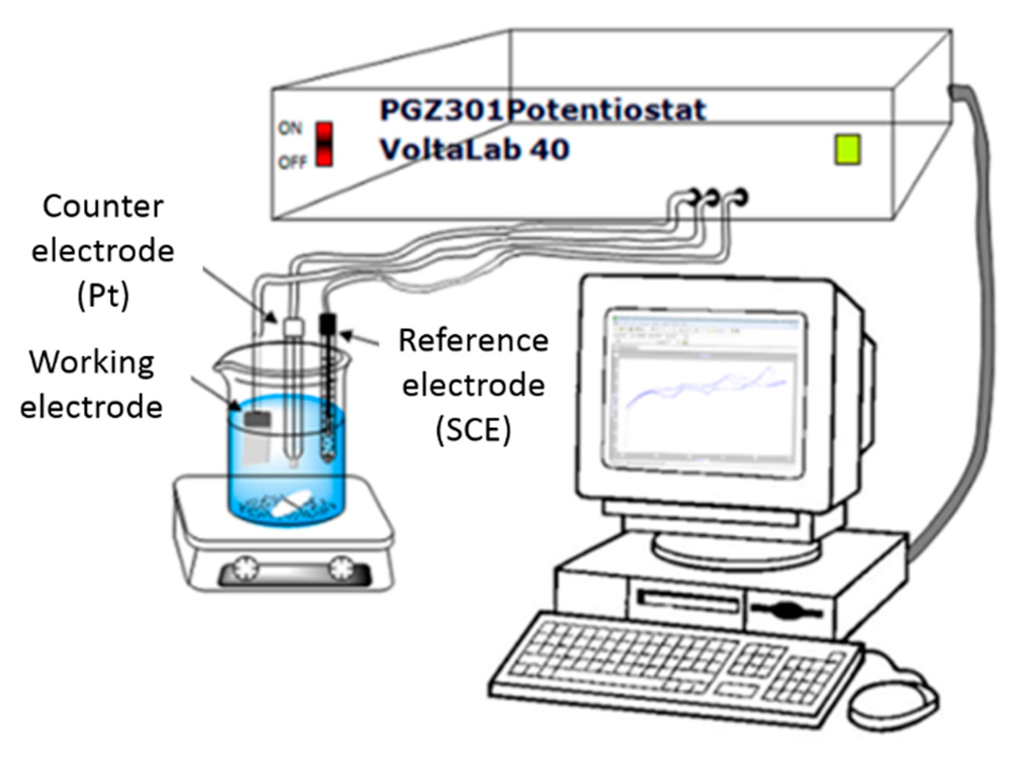
2. Materials and Methods

The electrochemical experiments were performed in a three-electrode cell configuration at room temperature. The cell contains a fluorine-doped tin oxide (FTO) coated glass substrate (7 Ω/sq) as the working electrode, a platinum grid as the counter electrode and a saturated calomel electrode (SCE) as the reference electrode. This system was controlled by a Potentiostat VoltaLab 40 (PGZ301 and VoltaMaster 4) (Figure 1). The substrates were ultrasonically cleaned with acetone and ethanol for 10 min each, rinsed with deonized water and dried.
The electrolyte solution contains 100 mM ammonium chloride (NH4Cl) as supporting electrolyte, 2 mM copper chloride (CuCl2), 2.5 mM selenious acid (H2SeO3) and 2 mM of antimony potassium tartrate (K2[Sb2(C4H2O6)2]·3H2O) as prescursors of Cu, Se and Sb respectively. The pH of the solution was adjusted to 2.00 ± 0.01 using concentrated HCl [14]. Linear sweep voltammetry (LSV) method was carried out to determinate the oxidation/reduction potentials of electrolyte solution. It is also used for a comparative study between Cu–Se, Sb–Se binary solutions and Cu–Sb–Se ternary solution. All voltammograms were measured at a scan rate of 5 mV/s over a potential range of −0.8 to +0.3 V/SCE. The chronoamperometry, an electrochemical technique in which the potential of the working electrode is fixed and the resulting current is monitored as a function of time, was then performed at the potential of −0.4 V/SCE without stirring for 30 min at room temperature to deposit the layers. The obtained samples were annealed in a quartz tube furnace at temperature of 250, 300, 350, 400, 450 and 500 °C for 15 min under nitrogen flow.
The structure of CuSbSe2 thin films was investigated using an X-Ray diffractometer (D8 Advance Twin, Bruker, Billerica, MA, USA), with Cu Kα1 radiation wavelength 1.5418 Å, with a sweep of 5° to 80° and a step of 0.02°. The surface morphology and chemical composition were studied by scanning electron microscope (SEM, Format JEOL/EO/Version 1.00, JEOL, Tokyo, Japan) and energy dispersive X-ray (EDX) detector. The optical properties of electrochemically grown films were tested using an UV/Vis double-beam spectrophotometer (V730, Jasco, Tokyo, Japan) with the light source of deuterium lamp (190 to 350 nm) and halogen lamp (330 to 1100 nm). Raman scattering measurements were performed using Bruker VERTEX 70 Raman spectroscopy, using a 532 nm excitation laser with a 0.95/100× objective; focused in a spot of ~1 μm in diameter. Operating at the maximum power of 30 mW and an accumulation time of 30 s.

3. Results and Discussion

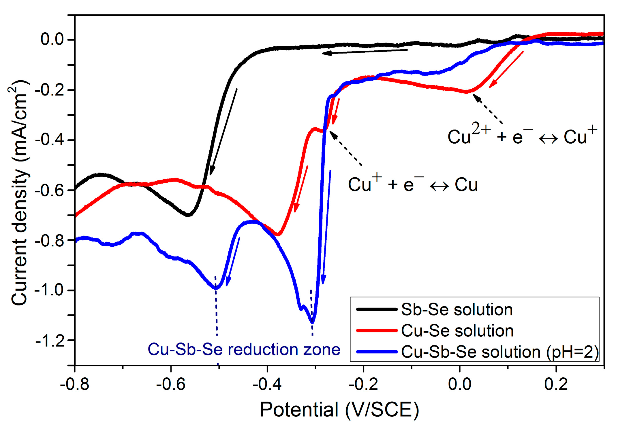
3.1. Linear Sweep Voltammetry

Figure 2 shows the voltammogram of FTO-coated electrode in the Cu–Sb–Se solution; the voltammograms of the Cu–Se and Sb–Se solutions are shown for comparison. A small increase in cathodic current was observed from the beginning of the sweep (+0.07 V/SCE), followed by a plateau between −0.03 V and −0.25 V/SCE. Compared to the Cu–Se solution, the voltammogram of the Cu–Sb–Se solution has no visible peaks corresponding to the respective reduction of Cu2+ and Cu+. This could be explained by their competition with other precursors for adsorption sites at the substrate [14]. After that, the cathodic current becomes larger at −0.3 V/SCE, which refers to a simultaneous deposition of Cu and Se as in the Equation (1) [20]. The second large cathodic peak of Cu–Sb–Se solution at −0.5 V/SCE corresponds to Sb–Se deposition as in Equation (2) [21]. It is interesting to note that the reduction peaks of the Cu–Sb–Se solution show a positive shift compared to the Cu-Se solution and the Sb–Se solution. This may be due to the fact that the presence of the three compounds together promotes the reduction process [14].
H2SeO3 + Cu2+ + 4H+ + 6e ↔ CuSe + 3H2O
3H2SeO3 + 2SbO+ + 16H+ + 18e ↔ Sb2Se3 + 11H2O
Since the electrodeposited films are very sensitive to potential variation, potentials between −0.30 and −0.48 V/SCE were tested by chronoamperometry [16] The deposition potential of −0.40 V/SCE was found to be the most suitable for the preparation of CuSbSe2 thin films yielding deposited films with a nearly stoichiometric composition.

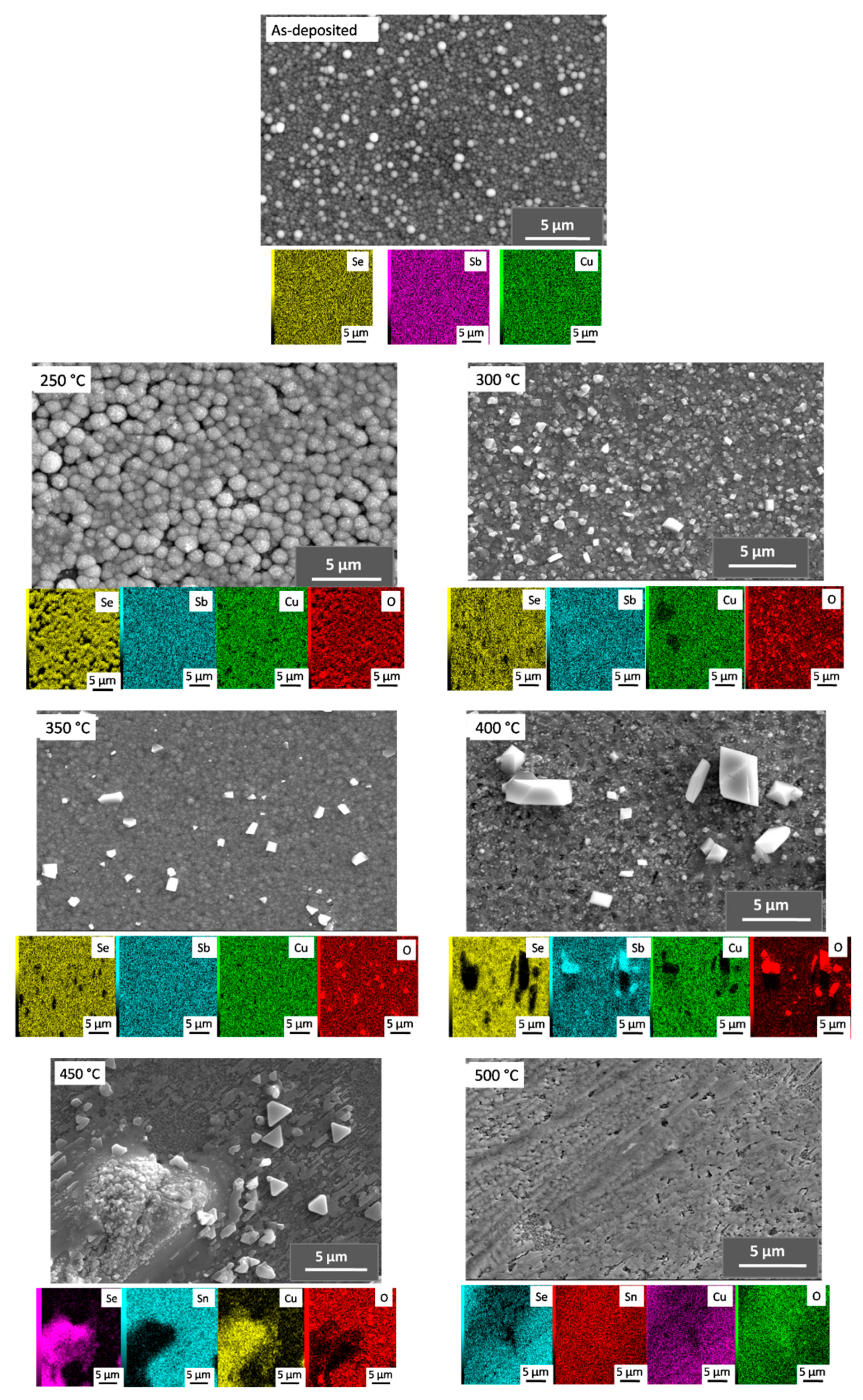
3.2. Morphological Characterization

The as-deposited Cu–Sb–Se thin film (Figure 3) exhibits a homogeneous and compact surface with spherical grains of 250 nm in size. The EDX analysis (Table 1) shows that the as-deposited samples are poor in copper and selenium. The annealing process changes the samples morphology depending on the temperature, in a drastic way (Figure 3). At 250 °C, the spherical shapes become disordered and thus expand to a diameter of 1250 nm, turning rough and cracking into small crystal grains with an average size of 125 nm. At 300 °C, the crystal grains continue to grow up to 400 nm in size. They then uniformly spread out on the surface of the substrate. At this temperature, some octahedrons, identified as Sb2O3 by EDX and XRD, start to appear. At 350 °C, the morphology of the deposit was significantly improved, more compact and uniform. From the SEM image, the grains size is reduced to 250 nm, which might be due to the compression effect during the layer growth. Few Sb2O3 crystals are present, even though their sizes increases. EDX analysis shows a sharp decrease in oxygen and a Cu/Sb ratio = 0.86, which increase to 0.91 if we consider the atomic % of Cu, Sb and Se only, close to the stoichiometric CuSbSe2 (Table 1). At 400 °C, the sample became porous with an even distribution of cavities, which could be attributed to the evaporated Sb2Se3 phase [22], resulting from the decomposition of CuSbSe2 as shown in Equation (3) [19]:
3CuSbSe2 (s) ↔ Cu3SbSe3 (s) + Sb2Se3 (g)↑
At 450 °C the layer shrinks and forms big agglomerates exceeding 10 microns in size, copper-rich and antimony-poor as shown by the EDS/mapping measurements. These agglomerates are surrounded by a thin layer of a deposit of Cu–Se and triangular grains with sizes from about 100 nm to ≥1 μm, likely Sb2O3, given their composition with ratio of Sb/O ~ 0.64. This strange morphology has been explained by Guo et al., suggesting that the annealing temperature approaches the melting point of CuSbSe2 (480 °C), the grain size increases progressively, and the small particles clustered together to form large block particles [23]. Finally, at 500 °C, the agglomerates diffuse into a fairly flat structure with a rail-like appearance and the grain boundaries became unclear in the SEM image. Visually, the layer is very thin. EDX analysis (Table 1) supports that the increase in Sn and Si content at 450 and 500 °C comes from the substrate, due to their exposure following the shrinkage and thinning of the deposits. Generally, from 400 to 500 °C, the Cu/Sb ratio was found to increase up to 3.86, suggesting that a part of the Sb might have been lost due to Sb2Se3 sublimation. However, the Sb/Se ration is less than 0.14, which could be explained by the fact that the selenium released from the dissociation of Sb2Se3 is recovered by other reactions to form Cu2Se contributing to ternary compounds formation, as in equations below [10,19]:
Sb2Se3 (s) ↔ 1/4Sb4 (g) + SbSe (g) + Se2 (g)
2Cu + 1/2Se2 ↔ Cu2Se (s)
3Cu2Se (s) + Sb2Se3 (s) ↔ 2Cu3SbSe3
SEM-EDS analysis is unable to separate if the detected oxygen comes from the substrate or from the remaining oxygen of the precursors or of the tube during annealing. However, it has been reported that crystalline Sb2O3 is formed during the reaction of Sb with O at temperatures in the range 270–360 °C [24]. Therefore, Sb2O3 octahedrons are not present on the as-deposited sample and on that annealed at 250 °C.

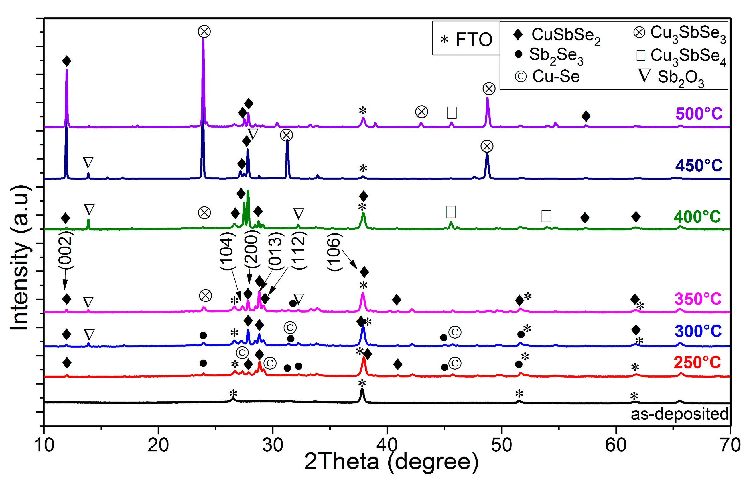
3.3. Structural Characterization

3.3.1. XRD Measurements

As demonstrated by the study of linear voltammetry, the electrodeposition of Cu–Sb–Se takes place in the form of binary compounds such as CuSe and Sb2Se3 (Equations (1) and (2)). Before the annealing process, the as-deposited sample have an amorphous nature with XRD diffraction peaks indexing only the substrate SnO2 (JCPDS 46-1088) as shown in Figure 4. After annealing CuSbSe2 thin films XRD patterns show the presence of mixed ternary and binary phases. CuSbSe2, Sb2Se3, Cu3SbSe3, Cu3SbSe4 and Sb2O3 compounds are mainly found in the prepared films.
At 250 °C, the weak intensity of peaks indicates a poor crystallinity of deposited films; it can also be noticed that the binary phases (CuSe and Sb2Se3) are predominant and that CuSbSe2 starts to form (peak at 27.8°). From 300 to 350 °C, Cu becomes involved in the diffusion processes and reacts, both with the selenium liberated by a partial decomposition of Sb2Se3 as expressed previously in Equations (4) and (5) and with CuSe (Equation (7)), which lead to the formation of Cu2Se (s).
Cu + CuSe ↔ Cu2Se (s)
The generated Cu2Se would further react with Sb2Se3 phase to form CuSbSe2 as expressed in Equation (8) [17]:
Cu2Se (s) + Sb2Se3 (s) ↔ 2CuSbSe2 (s)
At 350 °C, the two strong peaks centered at 28.8° and 27.8° are indexed to the (112) and (200) planes of CuSbSe2 phase (JCPDS 75-0992). In addition, the weak diffraction peaks indexed to (013) plane of CuSbSe2 phase, Cu3SbSe3 (JCPDS 086-1751) and Sb2O3 (JCPDS 75-1565) can also be observed. At 400 °C, Sb2Se3 sublimates to gradually leave the films, explaining the absence of the corresponding peaks in the XRD spectra [10]. However, there is a dominant presence of CuSbSe2 and Sb2O3 phases with a more sharper peaks centered at 27.8° and 27.5° corresponding respectively to the (200) plane of CuSbSe2 phase and the (222) of Sb2O3 phase. Besides a slight emergence of the Cu3SbSe3 phase at 23.87°, diffraction peaks at 27.3°, 45.5° and 54° corresponding to the Cu3SbSe4 phase (JCPDS 85-0003) also appeared at 400 °C. From 450 to 500 °C, the peaks at 23.93° and 48.93° attributable respectively to the (121) and (133) planes of Cu3SbSe3 phase become considerably intense and sharp. It can also be noticed that the peak at 11.9° belonging to the (002) plan of CuSbSe2 phase increased significantly.
As far as the crystallographic orientations vs. temperature concerns, the CuSbSe2 phase changes from the (112), (013) and (200) directions at 350 °C to a predominance of the (200) direction at 400 °C. At temperature of 450–500 °C, the CuSbSe2 phase changes predominantly to the (002) direction. These results are in agreement with the observations reported by Yang et al. [10], which also demonstrated that CuSbSe2-based solar cells with preferred (013)- and (112)-orientations show better efficiency, due to the easier carriers transport within the layers and to the lower recombination loss.

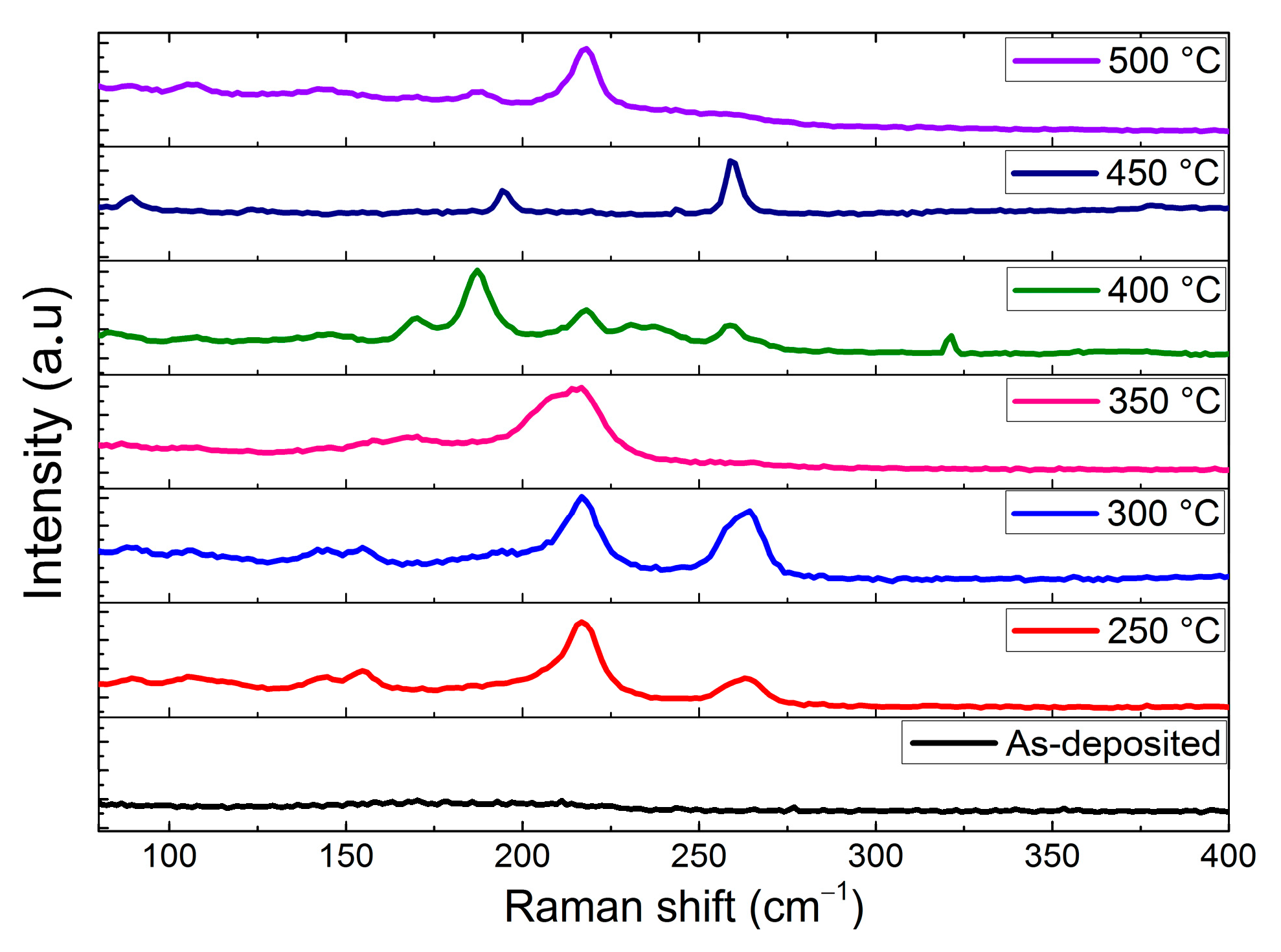
3.3.2. Raman Measurements

In order to further investigate the structural properties and to analyse the phase formation at different temperatures, Raman spectroscopy was performed on CuSbSe2 thin film, using 532 nm laser excitation sources in the wavenumber range of 80–400 cm−1.
The Raman spectrum of the as-deposited sample shows a very weak and broad peak, as shown in Figure 5 (Figure S4 in Supplementary Materials), which confirms that the electrodeposited and unannealed CuSbSe2 thin film is amorphous. However, the Raman spectra of the samples annealed at 250 and 300 °C show two strong peaks centered at about 217 and 264 cm−1 and four weak peaks at 89, 105, 144 and 154 cm−1. The Raman peaks at 217 (Ag), 154 (Ag), 144 (B2g), 105 (Ag) and 89 cm−1 (Ag) are assigned to CuSbSe2 phase [18,25,26]. The Raman peak at 264 cm−1 is ascribed to A1g of Cu2Se phase [27]. The peaks representing the Sb2Se3 phase are not distinguishable, but it appears that the peak at 189 cm−1 (Ag) due to Se–Sb–Se bonds of Sb2Se3 phase overlaps with the peak at 217 cm−1 (Ag) of the CuSbSe2 phase, resulting in an asymmetric peak broadning [9,25]. At 350 °C, the Raman spectrum is distinguished by two overlapping high peaks at 217 and 208 cm−1, corresponding respectively to Ag and B2g modes of CuSbSe2 phase [18,25]. This overlap can be attributed to a broadening of the peaks probably resulting from the high power of the laser used. Indeed, Kumar et al. [28], had recently studied the effect of the annealing temperature and the excitation power on the Raman spectrum of Sb2Se3. They mention that the laser heating effect always results in anharmonic effects in solids, evidenced by the broadening and redshift of the Raman bands. Besides, a weak peak corresponding to B1g mode of Cu3SbSe3 phase is also observed at about 167 cm−1 [25]. However, the peaks representing the binary phases of Cu2Se (264 cm−1) and Sb2Se3 (189 cm−1) disappeared, confirming their transformation into ternary phases at annealing temperature of 350 °C.
As previously demonstrated by SEM and XRD measurements, the annealing temperatures above 350 °C promote the formation of Cu-rich phases due to the loss of Sb associated to the sublimation of Sb2Se3. At 400 °C, the main peak at 187 cm−1 can be attributed to CuSe4/SbSe4 stretching vibrations of the Cu3SbSe4 phase as reported in [29,30] or to the Ag mode of the Cu3SbSe3 phase [9,25]; the peaks at 230 and 169 cm−1 correspond to Cu3SbSe4 [29]. It can also be seen that the minor peaks (83, 106 and 144 cm−1) corresponding to the CuSbSe2 phase reappear next to the main peak at 217 cm−1 which seems to decrease. The peak at 259 cm−1 corresponds to A1g mode of Sb2O3 phase [31]. While, the peak at 320 is unknown so far. At 450 °C, the highest peak at 259 cm−1 has been assigned to the Se–Se stretch vibration of the Se2− ions of Cu2Se phase [27]. However, the majority of peaks at 89, 194, 258 and 376 cm−1 belong to cubic Sb2O3, in agreement with the reported Raman modes [31]. The presence of Cu3SbSe3 and CuSbSe2 phases has not been identified, due to the poor intensity of their bands compared to other phases. At 500 °C, the peaks representing Cu3SbSe3 and CuSbSe2 phases reappear, respectively at 107, 144 and 217 cm−1 for CuSbSe2 and at 188 cm−1 for Cu3SbSe3 phase. The observed Raman modes of all samples are tabulated in Table 2.

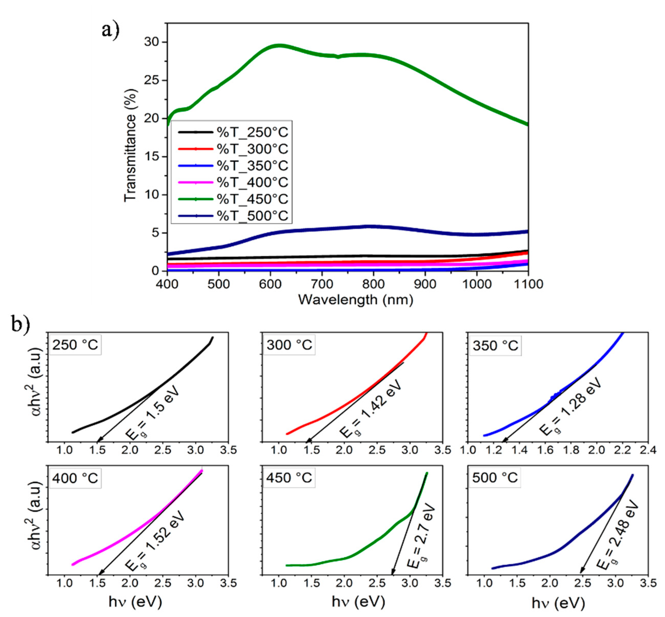
3.4. Optical Characterization

The optical transmittance spectra of all CuSbSe2 thin films were measured in the wavelength range 400–1100 nm as shown in Figure 6a and, as expected, they largely differ depending on the thermal treatment. All the annealed samples show high absorption in the visible to near-infrared (NIR) spectral region 400–900 nm with an optical transmittance ≤6%. However, the sample annealed at 450 °C has a transmittance reaching 30%, that could be due to the shrinkage of the films that uncovers the transparent FTO substrate, as shown by SEM/EDS measurements.
The variation of the optical direct band gap of CuSbSe2 thin films vs. annealing temperature is estimated by using the Tauc’s equation (Equation (9)), as shown in Figure 6b:
(αh𝜈)n = A(h𝜈Eg)
where α, h𝜈, A and Eg are the linear absorption coefficient, photon energy, a constant which related to effective mass and the band gap, respectively; n assumes the values of 2 for direct and 1/2 indirect transition. The optical band gap (Eg) can be derived from the extrapolation of the straight line part of the curve (αh𝜈)n vs. h𝜈 to (αh𝜈)n = 0.
It was observed that for all the samples, the best straight line is obtained for a value of n equal to 2, which is typical of direct allowed transitions [32,33].
The bandgap values of all the samples were higher than the expected value for CuSbSe2 (~1.1 eV [8]) and affected by the presence of other phases as indicated by the compositional analyses. For the samples annealed at 250 °C to 400 °C, that could be due to the existence of higher band-gap Sb2O3 (~3.5 eV) [34]. For the 450 and 500 °C annealed samples, it is due to morphological transformations. The smallest bandgap value of 1.28 eV belongs to the sample annealed at 350 °C, which is in agreement with the results reported by Colombara et al. [7].

4. Conclusions

The effect of the heat treatment on the evolution of electrodeposited CuSbSe2 thin films has been investigated by varying the annealing temperature from 250 to 500 °C. We showed that the phases, composition, morphology, optical properties and crystalline orientations of the Cu–Sb–Se films, were strongly dependent by the annealing temperature as shown by X-ray diffraction (XRD), scanning electron microscope (SEM), energy dispersive spectrometer (EDX) and Raman spectroscopy.
During the electrodeposition process, defined by voltammetry and chronoamperometry, single compounds such as Cu(s) and Sb(s) and binary compounds such as CuSe and Sb2Se3 are deposited on the substrate. The different annealing conditions lead to the assembly of these compounds and the formation of new products including CuSbSe2 phase and other ternary phases as well as antimony oxide.
These film characterizations indicate that the growth of single-phase CuSbSe2 thin films is feasible at temperature of 350 °C; the formation of Sb2O3 secondary phases, which might be detrimental to the performance of CuSbSe2-based solar cells, can be avoided by preventing oxygen sources during the electrodeposition and the annealing process or easily removed with diluted HCl acid (Supplementary Materials). The good optical properties of the 350 °C annealed film, combined to the simple, cheap and easily scalable deposition technique, make the electrodeposition a promising solution, in particular for the realization of CuSbSe2-based thin film solar cells.

Supplementary Materials

The following supporting information can be downloaded at: www.mdpi.com/article/10.3390/coatings12010075/s1, Figure S1: Illustration of the growth mechanism of CuSbSe2 thin films under annealing temperature effect, Figure S2: Grain size evolution during annealing process, Figure S3: SEM images of elelctrodeposited (−0.4 V/SCE/60 min) and annealed (350 °C) CuSbSe2 thin films: before and after chemical etching of Sb2O3 octahedrons by diluted HCl, Figure S4: Raman spectra of the as-deposited CuSbSe2 thin films.

Author Contributions

Conceptualization, K.A.; investigation, A.A., M.O., A.A.H. and L.B.; writing—original draft preparation, K.A. and L.A.; writing—review and editing, E.G. and A.S.; project administration, A.I., K.B. and N.L. All authors have read and agreed to the published version of the manuscript.

Funding

This research was partially funded by The Moroccan Ministry of Higher Education and Research in the framework of the CNRST (Morocco)/CNR (Italy) cooperation program: “Towards very low cost deposition of Chalcopyrite and Kesterite-based thin film solar cells: CIGS (Cu(In, Ga)Se2) and CZTS (Cu2ZnSn(S, Se)4)”.

Institutional Review Board Statement

Not applicable.

Informed Consent Statement

Not applicable.

Data Availability Statement

Not applicable.

Acknowledgments

The authors gratefully acknowledge R. Laghrib and M. Agnaou for the XRD and SEM measurements and L. Nkhaili for Raman measurements.

Conflicts of Interest

The authors declare no conflict of interest. All authors have participated in conception and design, or analysis and interpretation of the data; drafting the article or revising it critically for important intellectual content; and approval of the final version. This manuscript has not been submitted to, nor is under review at, another journal or other publishing venue. The authors have no affiliation with any organization with a direct or indirect financial interest in the subject matter discussed in the manuscript.

References

  1. Green, M.A.; Dunlop, E.D.; Hohl-Ebinger, J.; Yoshita, M.; Kopidakis, N.; Hao, X. Solar cell efficiency tables (version 56). Prog. Photovolt. Res. Appl. 2020, 28, 629–638. [Google Scholar] [CrossRef]
  2. Wang, W.; Winkler, M.T.; Gunawan, O.; Gokmen, T.; Todorov, T.K.; Zhu, Y.; Mitzi, D.B. Device characteristics of CZTSSe thin-film solar cells with 12.6% efficiency. Adv. Energy Mater. 2014, 4, 1301465. [Google Scholar] [CrossRef]
  3. Jiang, C.; Zhou, J.; Tang, R.; Lian, W.; Wang, X.; Lei, X.; Zeng, H.; Zhu, C.; Tang, W.; Chen, T. 9.7%-efficient Sb2(S, Se)3 solar cells with a dithieno[3,2-b :2′,3′-d]pyrrole-cored hole transporting material. Energy Environ. Sci. 2021, 14, 359–364. [Google Scholar] [CrossRef]
  4. de Souza Lucas, F.W.; Zakutayev, A. Research update: Emerging chalcostibite absorbers for thin-film solar cells. APL Mater. 2018, 6, 084501. [Google Scholar] [CrossRef]
  5. Hao, M.; Liu, Y.; Zhou, F.; Jiang, L.; Liu, F.; Li, J. CuSbS2 nanocrystals applying in organic-inorganic hybrid photodetectors. ECS Solid State Lett. 2014, 3, Q41–Q43. [Google Scholar] [CrossRef]
  6. Zhang, D.; Yang, J.; Jiang, Q.; Fu, L.; Xiao, Y.; Luo, Y.; Zhou, Z. Ternary CuSbSe2 chalcostibite: Facile synthesis, electronic-structure and thermoelectric performance enhancement. J. Mater. Chem. A 2016, 4, 4188–4193. [Google Scholar] [CrossRef]
  7. Colombara, D.; Peter, L.M.; Rogers, K.D.; Painter, J.D.; Roncallo, S. Formation of CuSbS2 and CuSbSe2 thin films via chalcogenisation of Sb–Cu metal precursors. Thin Solid Film. 2011, 519, 7438–7443. [Google Scholar] [CrossRef] [Green Version]
  8. Takei, K.; Maeda, T.; Wada, T. Crystallographic and optical properties of CuSbS2 and CuSb(S1−xSex)2 solid solution. Thin Solid Film. 2015, 582, 263–268. [Google Scholar] [CrossRef]
  9. Goyal, D.; Goyal, C.P.; Ikeda, H.; Malar, P. Role of growth temperature in photovoltaic absorber CuSbSe2 deposition through e-beam evaporation. Mater. Sci. Semicond. Process. 2020, 108, 104874. [Google Scholar] [CrossRef]
  10. Yang, B.; Wang, C.; Yuan, Z.; Chen, S.; He, Y.; Song, H.; Ding, R.; Zhao, Y.; Tang, J. Hydrazine solution processed CuSbSe2: Temperature dependent phase and crystal orientation evolution. Sol. Energy Mater. Sol. Cells 2017, 168, 112–118. [Google Scholar] [CrossRef]
  11. Wang, C.; Yang, B.; Ding, R.; Chen, W.; Kondrotas, R.; Zhao, Y.; Lu, S.; Li, Z.; Tang, J. Reactive close-spaced sublimation processed CuSbSe2 thin films and their photovoltaic application. APL Mater. 2018, 6, 084801. [Google Scholar] [CrossRef] [Green Version]
  12. Rampino, S.; Pattini, F.; Bronzoni, M.; Mazzer, M.; Sidoli, M.; Spaggiari, G.; Gilioli, E. CuSbSe2 thin film solar cells with ~4% conversion efficiency grown by low-temperature pulsed electron deposition. Sol. Energy Mater. Sol. Cells 2018, 185, 86–96. [Google Scholar] [CrossRef]
  13. Welch, A.W.; Baranowski, L.L.; Peng, H.; Hempel, H.; Eichberger, R.; Unold, T.; Lany, S.; Wolden, C.; Zakutayev, A. Trade-offs in thin film solar cells with layered chalcostibite photovoltaic absorbers. Adv. Energy Mater. 2017, 7, 1601935. [Google Scholar] [CrossRef]
  14. Tang, D.; Yang, J.; Liu, F.; Lai, Y.; Li, J.; Liu, Y. Growth and characterization of CuSbSe2 thin films prepared by electrodeposition. Electrochim. Acta 2012, 76, 480–486. [Google Scholar] [CrossRef]
  15. Tang, D.; Yang, J.; Liu, F.; Lai, Y.; Jia, M.; Li, J.; Liu, Y. One-step electrodeposition and annealing of CuSbSe2 thin films. Electrochem. Solid-State Lett. 2011, 15, D11–D13. [Google Scholar] [CrossRef]
  16. Abouabassi, K.; Ouafi, M.; Hssi, A.A.; Atourki, L.; Kirou, H.; Labchir, N.; Boulkaddat, L.; Gilioli, E.; Elfanaoui, A.; Bouabid, K.; et al. CuSbSe2 Thin Films Deposited from Aqueous Solution by Electrodeposition in One Step. In Proceedings of the 2019 7th International Renewable and Sustainable Energy Conference (IRSEC), Agadir, Morocco, 27–30 November 2019; Volume 2, pp. 1–4. [Google Scholar]
  17. Karup-Møller, S. The Cu–Sb–Se phase system at temperatures between 350° and 700 °C. Neues Jahrb. Für Mineral. Abh. 1999, 174, 277–292. [Google Scholar] [CrossRef]
  18. Xue, D.-J.; Yang, B.; Yuan, Z.-K.; Wang, G.; Liu, X.; Zhou, Y.; Hu, L.; Pan, D.; Chen, S.; Tang, J. CuSbSe2 as a potential photovoltaic absorber material: Studies from theory to experiment. Adv. Energy Mater. 2015, 5, 1501203. [Google Scholar] [CrossRef]
  19. Yan, H.; Xiao, R.; Pei, Y.; Yang, K.; Li, B. Structural, electrical and optical characteristics of CuSbSe2 films prepared by pulsed laser deposition and magnetron sputtering processes. J. Mater. Sci. Mater. Electron. 2020, 31, 644–651. [Google Scholar] [CrossRef]
  20. Carbonnelle, P.; Lamberts, L. A voltammetric study of the electrodeposition chemistry of the Cu + Se system. J. Electroanal. Chem. 1992, 340, 53–71. [Google Scholar] [CrossRef]
  21. Liu, F.; Li, J.; Yang, J.; Han, Z.; Jiang, L.; Lai, Y.; Li, J.; He, Y.; Liu, Y. Preparation and characterization of AgSbSe2 thin films by electrodeposition. J. Electrochem. Soc. 2013, 160, D578–D582. [Google Scholar] [CrossRef]
  22. Liu, X.; Chen, J.; Luo, M.; Leng, M.; Xia, Z.; Zhou, Y.; Qin, S.; Xue, D.J.; Lv, L.; Huang, H.; et al. Thermal evaporation and characterization of Sb2Se3 thin film for substrate Sb2Se3/CdS solar cells. ACS Appl. Mater. Interfaces 2014, 6, 10687–10695. [Google Scholar] [CrossRef]
  23. Guo, T.; Wang, D.; Yang, Y.; Xiong, X.; Li, K.; Zeng, G.; Li, B.; Ghali, M. Preparation and characterization of CuSbSe2 thin films deposited by pulsed laser deposition. Mater. Sci. Semicond. Process. 2021, 127, 105716. [Google Scholar] [CrossRef]
  24. Agati, M.; Gay, C.; Benoit, D.; Claverie, A. Effects of surface oxidation on the crystallization characteristics of Ge-rich Ge–Sb–Te alloys thin films. Appl. Surf. Sci. 2020, 518, 146227. [Google Scholar] [CrossRef]
  25. Tiwari, K.J.; Vinod, V.; Subrahmanyam, A.; Malar, P. Growth and characterization of chalcostibite CuSbSe2 thin films for photovoltaic application. Appl. Surf. Sci. 2017, 418, 216–224. [Google Scholar] [CrossRef]
  26. Penezko, A.; Kauk-Kuusik, M.; Volobujeva, O.; Traksmaa, R.; Grossberg, M. Observation of photoluminescence edge emission in CuSbSe2 absorber material for photovoltaic applications. Appl. Phys. Lett. 2019, 115, 092101. [Google Scholar] [CrossRef]
  27. Xue, C.; Papadimitriou, D.; Raptis, Y.S.; Richter, W.; Esser, N.; Siebentritt, S.; Lux-Steiner, M.C. Micro-Raman study of orientation effects of CuxSe-crystallites on Cu-rich CuGaSe2 thin films. J. Appl. Phys. 2004, 96, 1963–1966. [Google Scholar] [CrossRef]
  28. Kumar, A.; Kumar, V.; Romeo, A.; Wiemer, C.; Mariotto, G. Raman Spectroscopy and In situ XRD probing of the thermal decomposition of Sb2Se3 thin films. J. Phys. Chem. C 2021, 125, 19858–19865. [Google Scholar] [CrossRef]
  29. Martínez-Ortíz, P.; Lugo-Loredo, S.; Campos-Álvarez, J.; Peña-Méndez, Y.; Aguilar-Martínez, J.A. Growth and characterization of Cu3SbSe4 thin films through thermally diffusing Sb2Se3–CuSe by chemical bath deposition (CBD). Mater. Res. Bull. 2018, 102, 418–423. [Google Scholar] [CrossRef]
  30. Wang, C.; Wu, Y.; Pei, Y.; Chen, Y. Dynamic disorder phonon scattering mediated by Cu atomic hopping and diffusion in Cu3SbSe3. NPJ Comput. Mater. 2020, 6, 155. [Google Scholar] [CrossRef]
  31. Pereira, A.L.J.; Gracia, L.; Santamaría-Pérez, D.; Vilaplana, R.; Manjón, F.J.; Errandonea, D.; Nalin, M.; Beltrán, A. Structural and vibrational study of cubic Sb2O3 under high pressure. Phys. Rev. B 2012, 85, 174108. [Google Scholar] [CrossRef] [Green Version]
  32. Kim, S.; Kim, N.-H. Impurity phases and optoelectronic properties of CuSbSe2 thin films prepared by cosputtering process for absorber layer in solar cells. Coatings 2020, 10, 1209. [Google Scholar] [CrossRef]
  33. Tauc, J. Optical properties and electronic structure of amorphous Ge and Si. Mater. Res. Bull. 1968, 3, 37–46. [Google Scholar] [CrossRef]
  34. Shinde, Y.P.; Sonone, P.N.; Ubale, A.U. Synthesis and characterization of hexagonal and tetrahedral nanocrystalline Sb2O3 thin films prepared by chemical spray pyrolysis technique. J. Alloys Compd. 2020, 831, 154777. [Google Scholar] [CrossRef]
Figure 1. The three-electrode cell connected to the potentiostat.
Coatings 12 00075 g001
Figure 2. Voltammograms of FTO-coated electrode in Cu–Se, Sb–Se and Cu–Sb–Se solutions.
Coatings 12 00075 g002
Figure 3. SEM/EDS-mapping of CuSbSe2 thin films, electrodeposited at 0.4 V/SCE during 30 min: as-deposited and annealed respectively at 250, 300, 350, 400, 450 and 500 °C under N2 for 10 min.
Coatings 12 00075 g003
Figure 4. XRD patterns of the CuSbSe2 thin films deposited at 0.4 V/SCE during 30 min and annealed at different temperature for 10 min in N2 atmosphere. (*) = peaks from the FTO substrate.
Coatings 12 00075 g004
Figure 5. Raman spectra of the CuSbSe2 thin films deposited at 0.4 V/SCE during 30 min and annealed at different temperature for 10 min in N2 atmosphere.
Coatings 12 00075 g005
Figure 6. Transmittance spectra (a) and Tauc’s plots (b) for direct band gap determination of the CuSbSe2 thin films annealed at different temperature.
Coatings 12 00075 g006
Table 1. EDX measurement of annealed samples at different temperature: atomic % and ratios.
FormulaAtom%
Cu
Atom%
Sb
Atom%
Se
Atom%
O
Atom%
Sn
Atom%
Si
Cu/SbSb/Se
T °C
As-deposited13.5122.1334.913.2521.74ND0.610.63
250 °C17.3122.8636.79.3813.75ND0.760.62
300 °C16.7822.5836.0810.8313.72ND0.740.62
350 °C19.3422.3939.973.4514.86ND0.860.56
400 °C18.5814.3435.5415.1916.39ND1.290.4
450 °C12.843.3217.6124.3730.2211.623.860.19
500 °C8.75321.6418.537.5611.052.90.14
Table 2. Raman modes for CuSbSe2 annealed at different temperature.
Annealed SamplesRaman Shift
(cm−1)
Assigned SymmetryCorresponding Phase
250 and 300 °C89AgCuSbSe2
105Ag
144B2g
154Ag
217Ag
264A1gCu2Se
189B2gSb2Se3
350 °C208B2gCuSbSe2
217Ag
167B1gCu3SbSe3
400 °C187-Cu3SbSe4/Cu3SbSe3
169-Cu3SbSe4
230-
83AgCuSbSe2
106Ag
144B2g
217Ag
259A1gSb2O3
450 °C259Se-Se stretchCu2Se
89-Sb2O3
194-
258A1g
376-
500 °C107AgCuSbSe2
144B2g
217Ag
188 Cu3SbSe3
Publisher’s Note: MDPI stays neutral with regard to jurisdictional claims in published maps and institutional affiliations.

