Article

Improving Compactness of 3D Metallic Microstructures Printed by Laser-Induced Forward Transfer

1
Faculty of Engineering and the Nanotechnology Center, Bar-Ilan University, Ramat-Gan 5290002, Israel
2
Additive Manufacturing Lab, Orbotech Ltd., P.O. Box 215, Yavne 8110101, Israel
3
Institute of Nanotechnology and Advanced Materials, Bar Ilan University, Ramat-Gan 5290002, Israel
*
Author to whom correspondence should be addressed.
Crystals 2021, 11(3), 291; https://doi.org/10.3390/cryst11030291
Submission received: 15 February 2021 / Revised: 8 March 2021 / Accepted: 11 March 2021 / Published: 16 March 2021

Abstract

:
Laser-induced forward transfer (LIFT) has been shown to be a useful technique for the manufacturing of micron-scale metal structures. LIFT is a high-resolution, non-contact digital printing method that can support the fabrication of complex shapes and multi-material structures in a single step under ambient conditions. However, LIFT printed metal structures often suffer from inferior mechanical, electrical, and thermal properties when compared to their bulk metal counterparts, and often are prone to enhanced chemical corrosion. This is due mostly to their non-compact structures, which have voids and inter-droplet delamination. In this paper, a theoretical framework together with experimental results of achievable compactness limits is presented for a variety of metals. It is demonstrated that compactness limits depend on material properties and jetting conditions. It is also shown how a specific choice of materials can yield compact structures, for example, when special alloys are chosen along with a suitable donor construct. The example of printed amorphous ZrPd is detailed. This study contributes to a better understanding of the limits of implementing LIFT for the fabrication of metal structures, and how to possibly overcome some of these limitations.

1. Introduction

Additive manufacturing (AM) of metals is becoming increasingly widespread with the emergence of 3D devices and the new complex, flexible and wearable electronics [1,2]. One of several AM methods for 3D metal printing is the laser-induced forward transfer (LIFT). LIFT is a non-contact digital printing method allowing the deposition of a wide range of metals in their bulk form [3]. With LIFT, a pulsed laser is focused through a transparent substrate onto a thin metal coating layer, typically 10’s to 100’s nm thick, often labeled the ‘donor’. When conditions are properly set (pulse width, spot size, energy), the absorbed pulse drives the jetting of a single molten droplet, typically at a rather high speed (10’s–100’s m/s) and angular accuracy, towards the target substrate. Consequently, one can accurately deposit a large number of droplets and create free-shape 3D structures [4,5,6]. As a single-step technique, LIFT does not typically require any post-treatment. One of the main advantages of LIFT is it’s high-resolution, with femtoliter droplet volume yielding a controllable droplet size of 0.5 µm to 15 µm on the target that is deposited at high accuracy [7]. All the mentioned advantages of LIFT make it a promising AM method for high-resolution and complex 3D structures [8]. Recent LIFT studies have demonstrated the printing of various 3D objects, e.g., high aspect ratio pillars and functional devices such as thermocouple [9] and thermal actuators [10]. Over the past few years, LIFT has been shown to have matured enough to be implemented as an exclusive open defects repair tool [11] serving in the printed circuit boards (PCBs) industry.
Despite all the advantages, the LIFT of metals often has limitations when it comes to its electrical and mechanical properties, which appear to be inferior to their bulk counterparts [12,13]. Therefore, its use in advanced applications such as microelectromechanical systems (MEMS) and flexible devices is still limited. Previous studies have shown that the electrical resistivity of LIFT printed structures is ~×3–~×10 inferior to the bulk value [12]. In some metals, such as aluminum, which readily oxidize in normal atmospheric conditions, even during the short duration of LIFT jetting (~µs), the resistivity increases up to ~×100′s times that of bulk Al [14]. Optimizing the physical system parameters (i.e., pulse energy, pulse duration, laser spot size, etc.) and printing conditions (the gap between donor and acceptor, metal layer thickness, etc.) can improve the electrical performance, eventually yielding low resistivity. For example, for printed copper, the resistivity can be reduced down to ~×3 bulk [12]. The post-printing thermal annealing treatment can decrease the resistance further to ~×2 bulk by increasing the metal grain sizes [15]. Though, such thermal treatment is limited to high-temperature substrates. Studies of the mechanical properties of the LIFT of copper and gold show that Young’s modulus of printed structures is ~×3 to ~×9 times lower than the bulk metal value [13]. Typically, LIFT printed metal structures are found to be brittle. The formation of metal-oxides at the droplet boundaries during the LIFT process occurs at readily oxidizable metals (such as aluminum and zirconium). In other metals such as copper or palladium, the amount of metal-oxides is negligible and its value is under the reliable detection threshold of analysis tools such as energy-dispersive X-ray spectroscopy (EDS) and x-ray diffraction (XRD). Therefore, in those metals, the metal-oxide, if it exists, is unlikely to be the major reason for the gap in the electrical and mechanical properties between the printed metals and their bulk form [14,16]. Both the low electrical conductivity and inferior mechanical properties have common origins: high porosity, low bonding strength, and delamination between the droplets. As previous studies have shown, fast solidification of the metal droplets has a clear effect on the morphology [17]: small grain sizes and air voids. The fast solidification of fL droplets arrests the spreading of the droplets and not the surface tension or viscous effects [18]. Porosity can also be controlled and improved to a certain level by adjusting the printing algorithm [4,12]. Yet, so far, full compact structures have not been demonstrated by using LIFT. It leads to the assumption that eventual compactness seems to be limited by the physical properties of the printed metal droplets. Another challenge is found in the droplets’ interface. In cross-section images of LIFT printed structures, one can clearly see a border that indicates the lack of interface between droplets. Different grain sizes are often seen on both sides of the interface between two droplets. In addition, delamination often takes place giving rise to air gaps between drops. One can predict the interfacial properties using a rather simple model based on the thermal properties of the metal [19].
Here, we describe a study of the physical effects leading to delamination, void formation, and lack of inter-melting between droplets during LIFT of 3D structures. High-resolution scanning electron microscope (HR SEM) images of focused ion beam (FIB) cross-sections made in printed samples contribute to understanding these effects [8,20]. Theoretical explanations, as well as experimental results, were used in elucidating the morphology and help draw limits to possible compactness achievable in the LIFT of metals. In most cases, it is quite impossible to completely avoid porosity, however, with the LIFT of metal glass [16], a highly compact structure can be achieved. Overcoming the inherent shortcomings to get compact structures is a key factor for high-quality LIFT printing and its industrial implementation. Some potential solutions in this direction are described.

2. Materials and Methods

The schematics of the LIFT printing system we have used were previously described [10,16]. We employed a fiber laser with a frequency doubling module providing 532 nm pulses with a tunable duration between 3 and 50 ns (VGEN, Spectra-physics, Rehovot, Israel). A Gaussian spot with a fixed spot size of ~35 µm (4σ) was used for jetting. The distance between the donor and the acceptor (the gap) was set to 400 µm. A sputtering system (SemiCore SC450, Livermore, CA, USA) served for the donor’s preparation by metal layers deposition on 1 mm thick glass slides.
Several such donors were prepared with Au, Cu, Ni, Pd, Bi, and ZrPd layers. In each case, printing conditioners were first tested and optimized to obtain the desired ‘single droplet jetting regime’. Process optimization includes testing various metal layer thicknesses and changing the pulse energy, typically in the range Ep = 1–15 µJ, and pulse width, tp = 1, 3, 5, 10, 20, 30, 40, 50 ns. Best conditions for quality jetting were then selected for printing test samples (square shapes metal slabs typically). Typically, the maximum pulse energy was chosen which still gives clearly distinguishable droplets with a minimal number of satellites as found in the droplet matrix printing tests [12]. The specific laser printing parameters used in each of the different cases are shown in Table A1 (Appendix).
Cross-sections (CS) of the printed structures were prepared using a dual-beam FIB-SEM system (HeliosNanoLab, FEI, Milpitas, CA, USA). High-resolution images of the resulting CS were further analyzed in order to evaluate the influence of the printing parameters and optimize the LIFT conditions.

3. Results

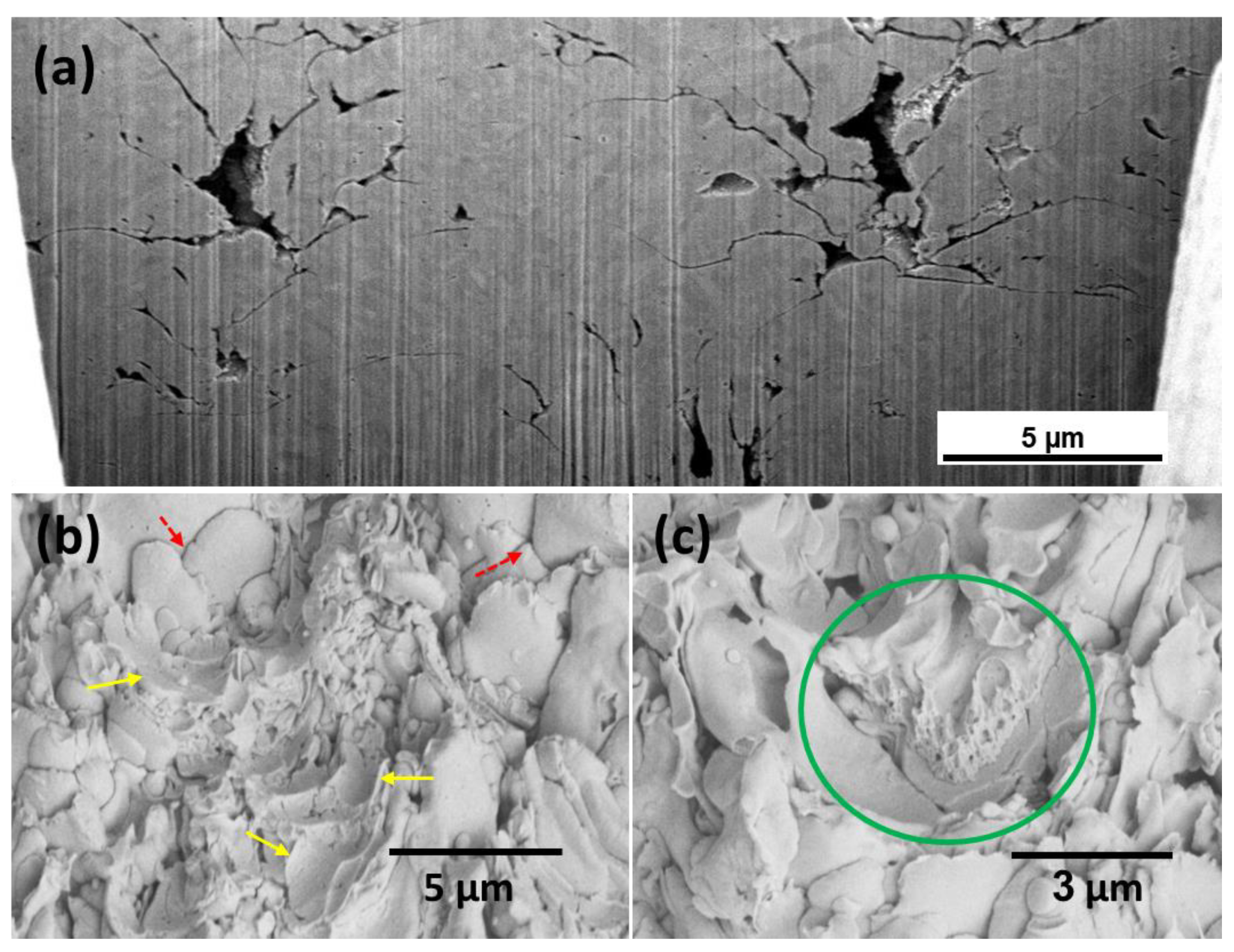
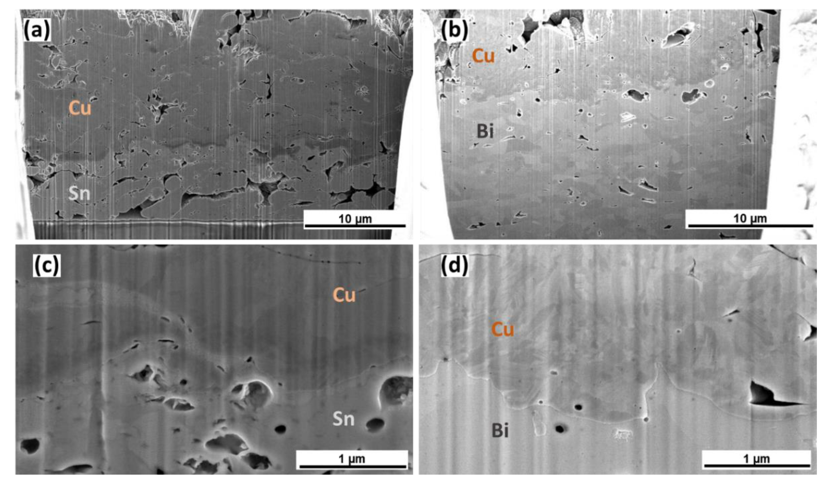
3.1. Voids and Delamination

The LIFT system was used to print the metal structures in this study. The laser energy in the printing process was either reflected or absorbed in the donor since the metal layer thickness was too thick for transmission of the light at 532 nm. The absorbed laser energy in the process was:
E T = E p · A  
where Ep is the laser pulse energy and A is defined by:
  A = ( 1 R g l a s s ) · ( 1 R m e t a l )
where Rglass is the reflectivity of the laser from the glass in the donor (~4%) and Rmetal is the reflectivity of the light (532 nm) from the metal. The value of Rmetal and the calculated value of A are summarized in Table A2 (Appendix).
LIFT printed metal structures typically contain voids, from trapped air or delamination. FIB polishing was used to get high-quality cross-sections which also revealed clear boundaries between the droplets. Figure 1a depicts a typical example of such a cross-section in printed copper. One can see the trapped air pockets as well as the delamination between droplets. The latter is seen as narrow lateral gaps between the flattened copper droplets that pile up. These gaps are expected to be the prime reason for the observed brittleness. To validate this, a fracture experiment was performed on a copper sample 1mm long and 200 µm thick, printed on FR4. The sample was pulled along its long axis until it broke. The SEM image of the fracture is shown in Figure 1b,c. The red arrows in Figure 1b indicate stacked, disc-like flat copper droplets with no clear indication of inter-melting. The yellow arrows point to areas where the fracture involves the separation of whole droplets, indicating the low bonding strength between the droplets. There were some areas of bulk-like fractures [21] that were demonstrated in the rough, coarse regions seen within the green circle in Figure 1c. The fact that such regions were rather rare could explain the brittleness of such printed structures.
Droplet delamination results from shear stress which develops as the droplet solidify on the metal substrate. The femtoliter droplets first spread out, attaining a ~1 µm thick, disc-like shape, which instantly solidified (i.e., within nanoseconds). There was almost no interfacial melting, as evidenced by SEM cross-sections, where a clear boundary was present between droplets. Delamination and air gaps were observed between droplets. There was a large density difference (~10%) between the liquid and solid phases of copper (ρS > ρL), and as the droplet solidified, shear stress developed at the border which could lead to partial delamination. The degree of this effect, which depended on the printing conditions, was encountered in a rather large number of printed metals. Still, it was not as universal as we will show below. To explore the role of metal properties and printing conditions, we studied several representative metal cases. Figure 2 depicts FIB cross-section images prepared from four LIFT deposited metal slabs: gold, nickel, palladium, and bismuth. Note that the typical diameter of the droplets was 5–10 µm and the height was 0.5–1 µm. The metal grains could be seen well in this figure. The grain sizes of the printed metal were affected by the cooling rate of the droplets when they reached the surface. The cooling rate was affected by the thermal properties of the metal and the material of the ‘acceptor’. As with the case of copper presented earlier, here as well, clear boundaries and voids were seen in printed Au, Ni, and Pd (Figure 2a–c). The deposited droplets maintained their shape and could easily be identified. Additionally, significant delamination was evident as represented by air gaps. However, in the case of the extraordinary metal, Bismuth, a different picture emerged. A highly compact structure was obtained with only a few voids and delamination (Figure 2d). Unlike the other three metals, its density in the liquid state was higher than the solid-state (ρS < ρL). It was due to this property that shear stress did not develop at the interface during solidification which otherwise would lead to delamination and void formation. This supports our assertion that voids seen in most other cases originate from the fast solidification during droplet spread-out, while no inter-droplet melting takes place. This, when combined with normal density change (ρS > ρL), leads to shear stress which partially tears off the deposited droplet leaving an air gap behind.
Another challenge facing quality metal LIFT printing has to do with minimizing trapped air voids. These, while mainly due to the fast solidification, strongly depend on the printing algorithm used, that is, the arrangement, ordering, and the number of droplets per unit area. Optimizing the printing algorithm can reduce the density and size of the voids. In our study, we applied the algorithm described earlier [4]. As mentioned, we maintained the highest possible pulse energy for droplet jetting while still avoiding sputtering. This, along with a large laser spot size, typically ~30 µm, which keeps a stable and large working window, yielded droplets with high kinetic and thermal energy. Such droplets could spread farther and solidify slower [12], this also serves to minimize voids.
The printed slab compactness, and consequently its strength, depends on both trapped voids and interfacial delamination. As demonstrated by the fracture test, the lack of inter-droplet melting, delamination, and voids contributed to its fragility. We further studied three different metals, with different liquid to solid density ratios r = ρsolidliquid. Slabs of palladium, copper, and bismuth were printed, where ρsolid was higher than ρliquid by 15.8%, 11.7%, and −2.7% respectively. Figure 3 shows the differences in voids’ characteristics. The higher the ratio (r) was, the larger the area of the voids were (the voids’ partial area was calculated from the projected 2D cross-sections). Bismuth demonstrated the highest compactness with minimal voids and no indication of delamination as expected from its anomalous density, while its low melting temperature increased the droplet solidification time.

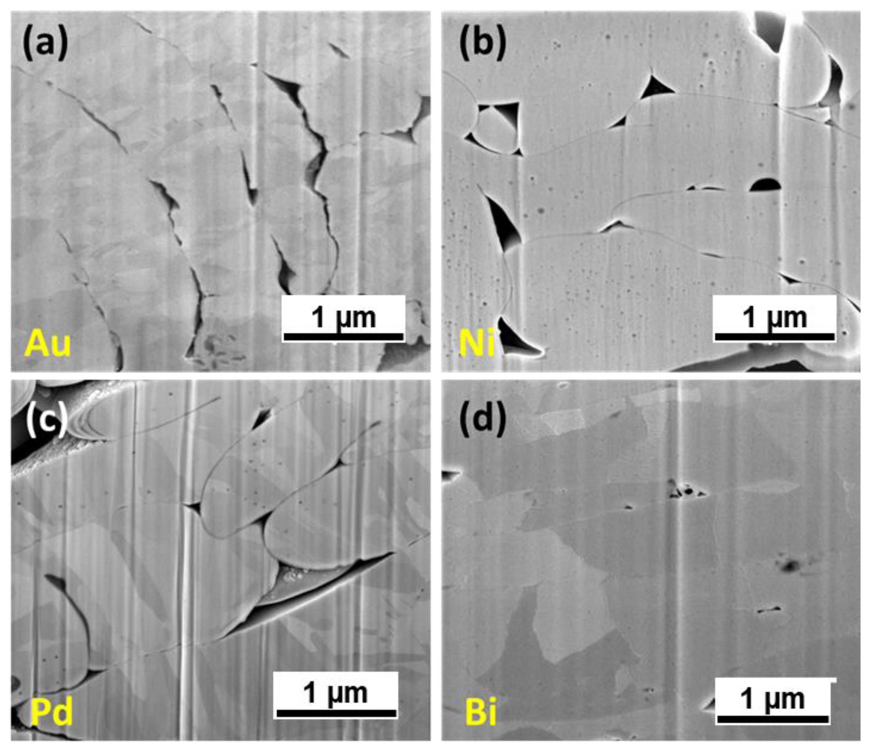
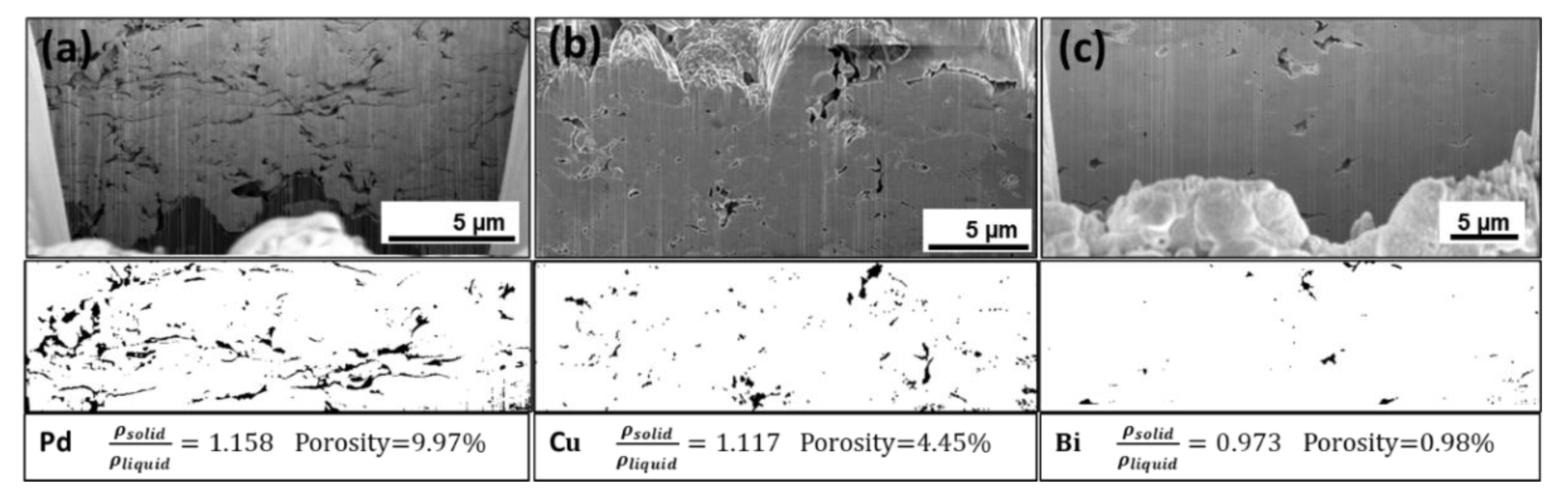
3.2. Inter-Droplet Melting
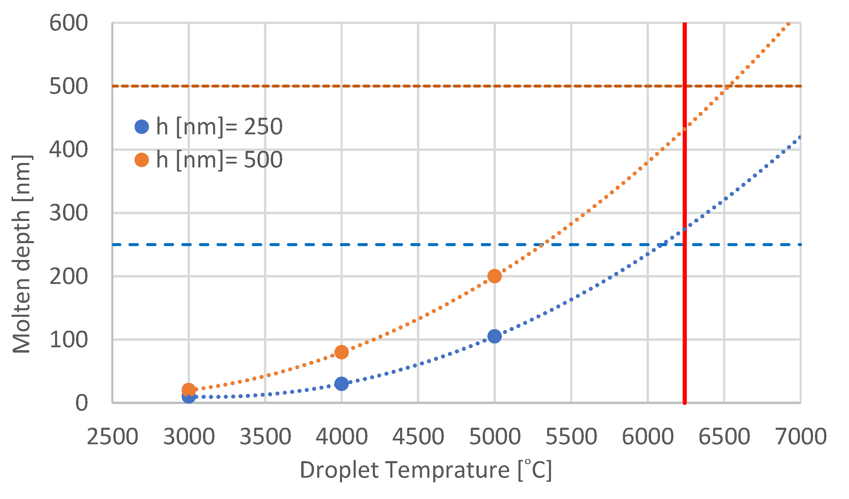
3.2.1. Theory

The lack of interfacial melting was mentioned as a major factor in the fragility seen in the LIFT printed structures. The molten metal droplets usually lacked enough thermal energy to induce the melting of the substrate. Clear interfacial boundaries were seen in the cross-sectional images (see e.g., Figure 2). HR-SEM images showed that the grains almost never crossed the droplet boundaries. In some cases, there was an indication of a thin interfacial layer of metallic glass that formed around the droplets [12].
The problem of melting a solid material in contact with its molten phase was dealt with by Stephane [22], then Neuman provided a solution for the melt at a temperature higher than Tm [23]. A mathematical analysis and solution were provided for the melt front propagation (X(t)) where the melt temperature is kept constant. Hu [24] used it to study structures built-up from molten tin droplets. The derivation starts with Stephan’s condition [22]:
k s T s x k l T l x = H f · ρ · d X ( t ) d t
where TL, Tm, and Ts are the molten liquid temperature, the metal melting temperature, and the substrate temperature respectively, and ks, and kl are the thermal conductivity coefficients of solid and liquid respectively, and Hf is the heat of fusion, and ρ is the density. X(t) describes the melt front evolution as a function of time.
In the case of LIFT printing that involves a small liquid volume (100’s of femtoliters typically or smaller), a very fast cooling rate (>~1010 K/s), and a high initial temperature of the molten metal (Td,0 >> Tm), a large temperature gradient results when landing on a metal substrate, which is typically near room temperature (since the cooling rate is far higher than the jetting rate). Additionally, the droplet spreads at a pace faster than the thermal conduction, and a thin layer is formed. The condition of fixed temperature at the boundary (X = 0), as required [24,25] for the analytical solution, therefore does not hold. To illustrate this, it is noted in [24] that the melt front propagation is given by:
X ( t ) = 2 λ α 1 t
where λ is a dimensionless number that is obtained from the solution to a transcendental equation (Equation (13) in [24]). Thus, a melt front will propagate whenever Td > Tm, only its propagation rate varies. This is not the case with the LIFT printing of small droplets, where the assumption of fixed temperature at the interface cannot be maintained. To deal with LIFT printed droplets inter-melting, a different approach is needed. We can derive an approximate solution starting from the Stephane conditions (Equation (3)). We consider two thin metal slabs in contact, one a solid metal at room temperature, the other, a molten metal layer at temperature T = TL (>Tm). Both slabs are of thickness h, typically 100’s of nanometers thick, that is, very thin. In this case, we can write Equation (3) as follows.
k s Δ T s k l Δ T L = H f · ρ · d X ( t ) d t · h
where h is the layer thickness. The liquid front progression is determined by the thermal diffusion, so we can write:
  d X ( t ) d t = 2 α s   X ( t )
where αs is the heat diffusion coefficient of the solid. From Equation (6) we can estimate the droplet temperature which is required to melt the substrate to a depth X(t) = h, equivalent to the droplet thickness itself. As ki = αi·cp·ρi, (cp,s, cp,l are the heat capacities of the solid and liquid respectively, αs, αl are the heat diffusion coefficients of the solid and liquid respectively), we can get this with the help of Equations (5) and (6), an equation for ∆TL = TLTM.
( T L T M ) = k s , d k l · [ ( T M T 0 ) + 2 H f c p , s ]
Equation (7) can be rewritten to account for supercooling as expected in several cases of interest, for example, when printing metal glasses [20]:
( T L , s c T M ) =     k s , d k l · [ ( T M T 0 Δ T s c ) + 2 H f c p , s ]
here ∆Tsc is the excess cooling temperature.
Equation (7) served to evaluate the temperature of an impinging molten droplet TL, which was required for interfacial melting. The ratio of the thermal conductivity of the solid-state to that of the liquid state ws detrimental to melting the substrate surface. Metals typically have their solid thermal conductivity much higher than the liquid. For interfacial melting to occur, the temperature of the droplet should be high enough to compensate for this difference in thermal conductivity. Note that here, ks,d designates the thermal conductivity of the solidified droplets, forming the substrate. Typically for LIFT printed structures, the thermal conductivity is lower than the bulk metal value as previous studies [12] have shown. This is due to the presence of inter-droplet boundaries and air gaps. As far as our simplified model was concerned, such differences might be negligible to the first approximation when we considered thin shell melting only, that is on the order of droplet thickness. Table 1 summarizes the calculated droplet temperature which will be required to satisfy substrate melting according to Equation (7). The thermophysical parameters used for the calculation are summarized in Table A3 (Appendix). In evaluating TL, we have assumed that the thermal conductivity of the printed substrate equals the bulk metal value, ks,d = ksolid, bulk. The calculated ΔTL is an upper limit given the assumption made in taking the bulk conductivity value. Table 1 shows results for both ks,sub = ksolid and assuming a twice lower thermal conductivity, ks,d = ks,bulk/2, to reflect a factor ×2 lower thermal conductivity of the printed substrate.
The droplet temperature required to melt the substrate according to Equation (7) is very high for most cases, and unattainable in LIFT printing which targets the droplet jetting regime. Even for Bismuth, which demonstrates printed structures with high compactness and lacking delamination, still, inter-droplet borders were evident in some cases as seen in high magnification, without interfacial grain crossing (Figure 2d, Figure 3c). Thus, for Bismuth as well, the required ∆TL was too high for the droplets to attain within the fully effective droplet jetting regime.
Stephane’s equation served above to obtain an estimate of the metal droplet’s excess temperature required to melt a substrate of the same metal. It was derived for the case where the melt front achieving a depth on the order of the droplet thickness, typically ~1 µm in the cases studied here. A better estimate of the required droplet temperature should be obtained from a numerical calculation of the thermal evolution making simple assumptions. A 2D model was employed to solve the thermal evolution, without flow, using COMSOL (Burlington, MA, USA) modeling software. Specifically, we have modeled a molten copper disc of thickness h on a solid copper substrate and traced the temperature evolution given an initial temperature T0. Figure 4 depicts the melting depth as a function of the copper droplet temperature for two cases of initial droplet thickness: h = 250 nm and h = 500 nm. Also shown is the droplet temperature obtained from Equation (7) for full melting (see vertical red line). The comparison with the COMSOL simulation results was quite good. One could notice that a significant melting of more than only a few nanometers started only at temperatures higher than a temperature that is above the boiling point of copper (2575 °C). It seems that there was no possibility of full melting in our case since the copper droplets could not be at such a high temperature.
We noted that to melt the interface and get interfacial co-solidification, the required melt depth could be smaller than the droplet thickness. Therefore, the temperatures calculated by Equation (7) were an overestimation. For example, we could learn from Figure 4, that for a droplet thickness of 500 nm, one already got a ~20 nm melting depth for a droplet at T = 3000 °C. While this was already a much higher temperature than typical droplet jetting conditions allow, it was still not clear whether such a thin melting layer could induce interfacial co-solidification and grain crossing.

3.2.2. Experimental Results
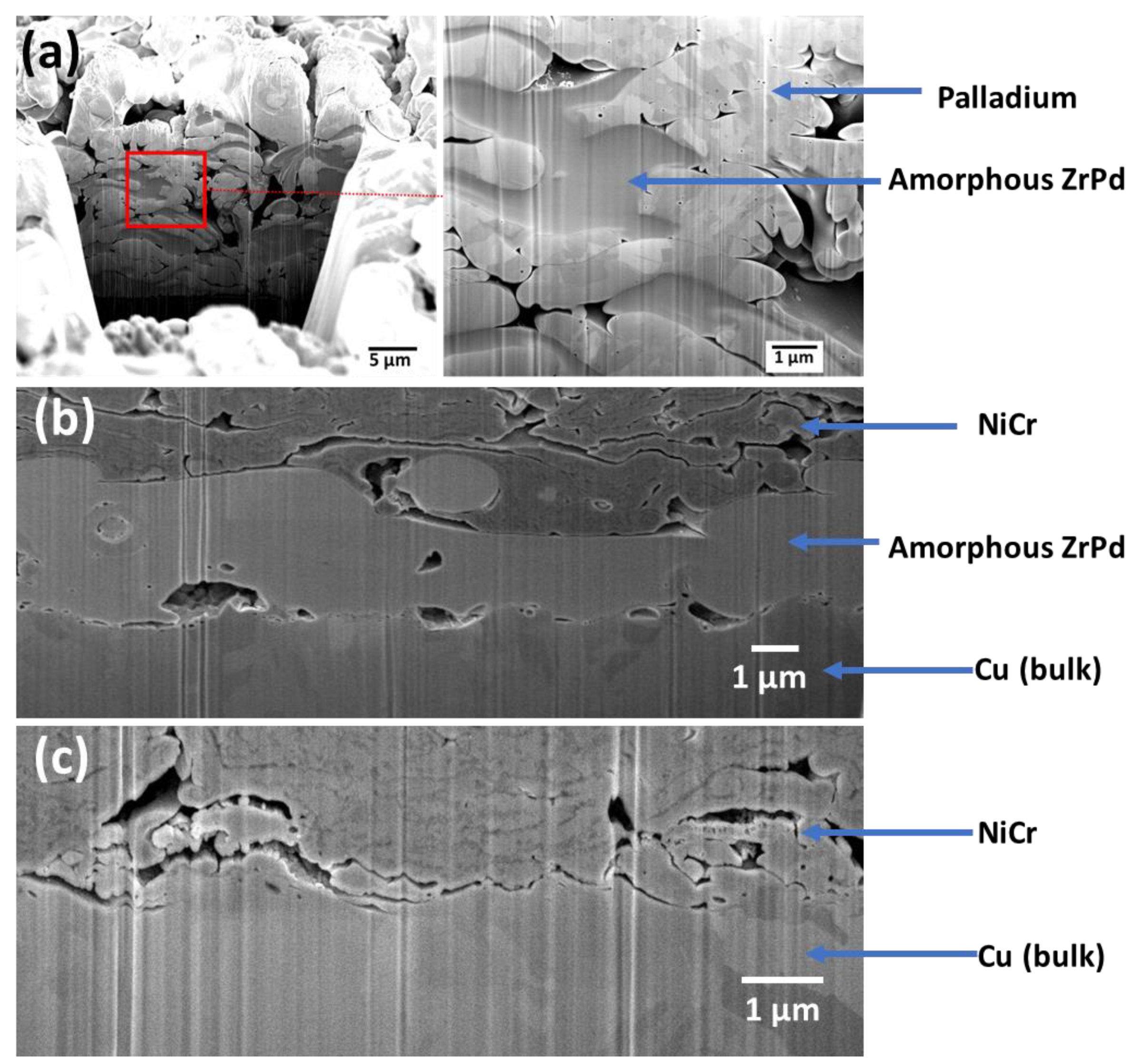
Interfacial melting initiated by the landing molten droplets on already solidified droplets is seen to be rare in LIFT metal printing. This was evident from the boundaries between the droplets, seen in the high-resolution SEM of cross-sections (Figure 2). While this is the typical case with homogenous metal structures, when printing heterogeneous structures such a drawback can be eliminated. This amounts to the printing of two, or more, different metals, for example, jetting droplets of a high melting temperature metal (Metal A) along with a low melting temperature metal (Metal B). This can possibly initiate interfacial melting. Consider tin or bismuth as Metal B on top of which droplets of Metal A are printed. As seen in Table 1, the required droplet temperature to melt Sn or Bi was ~1000 °C and ~600 °C respectively, temperatures which could not in principle be achieved in LIFT printing of Sn or Bi since they are >60% above their respective Tm. However, those temperatures could be achieved in LIFT of e.g., copper or many other relevant high Tm metals. Figure 5 shows cross-sections of such bi-metal structures, with copper deposited on printed Sn or Bi. While the porosity of both copper and tin was still evident (Bi demonstrates compactness, as discussed above), the interface between copper and either Sn or Bi was seen to be free of voids, no delamination was seen, as well as Cu diffusion and Cu penetration into the Sn or Bi (Figure 5c,d). This suggested that interfacial melting was taking place. There was also evidence of CuSn mixed phases at the interface which could be seen as a gradual discoloration between the Cu and the Sn (Figure 5c), while no mixed phases were seen at the copper-bismuth interface (Figure 5d). This reflected the respective phase diagram characteristics, where copper had a common solid phase with tin, but not with bismuth.

3.3. Metal Glass

Recently we demonstrated LIFT printing of amorphous ZrPd [16]. Such printed metallic glass (MG) showed morphological compactness due in part to the similarity in solid and liquid phases density, with their ratio as only ~1–2%. Consequently, there was a significant decrease in the number of voids. The droplet’s temperature depended on the melting temperature of the donor’s metal constituents. In our case, the donor was made of alternating layers of Zr and Pd [16]. While the Zr was the first deposited metal on the glass and the melting temperature of the metals were Tm(Zr) = 1855 °C, and Tm(Pd) = 1555 °C. Therefore, the droplet temperature was much higher than what would be obtained when jetting from a solid ZrPd alloy, where it was Tm ~ 1300 °C [26]. Moreover, during the jetting process, the Zr and Pd metal layers, intermixed to form the ZrPd alloy, and heat was generated due to their negative mixing enthalpy, ∆Hmix = −91 kJ/mole [27]. This would increase the droplet temperature further, by ~1000 °C. All in all, the ZrPd droplets should have a large excess temperature of over ~2000 °C, and this gives rise to the conformal structure observed with such printed MG structures. The droplet’s thermal energy was high enough to bring the substrate glassy phase above its glass transition temperature (Tg ~ 438 °C [28]) and promote compact interfacial bonding. When hit and heated by a high-temperature droplet, the MG substrate was readily heated above its Tg by the supercooling droplet and brought into a viscous liquid regime [29]. In this regime, the metallic glass was malleable and shapeable and thus the printed droplets could flow and form compact interfaces.
As explained above and shown previously [16], metal-glass structures could be LIFT printed to form compact structures. They can also serve as complementary adhesion materials when printed along with a crystalline metal. Figure 6 demonstrates two such cases. In the first case (Figure 6a), we printed a mixed structure made from droplets of amorphous ZrPd printed alongside crystalline Pd droplets. LIFT printed Pd is typically accompanied by voids, however, as one can clearly see, when mixed with the amorphous ZrPd phase, the latter permeated and filled the voids, forming a compact heterogeneous material. Depending on the specific design rule, materials ratio, and deposition scheme (print-plan), one can target such mixed material structures which are of desirable properties. In another realization, the printed MG served as an adhesion layer between two otherwise crystalline metals. Such a case is depicted in Figure 6b, where the amorphous ZrPd was LIFT printed as an intermediate layer between laminated bulk copper (bottom material) and LIFT printed NiCr (on top). In comparison to the case where NiCr was directly printed on the copper substrate (Figure 6c), one can appreciate here the improvement obtained by such an intermediate layer. Printing NiCr directly on copper was seen to result in interfacial air gaps, due mainly to delamination as discussed above. However, when an amorphous ZrPd layer was introduced, one could obtain bonded areas with better coverage on both sides which can lead to better adhesion.

4. Discussion and Conclusions

We dealt here with a well-known problem in LIFT printing of metals, namely, that printed 3D structures display a considerable number of voids due primarily to fast micro-droplets cooling, lack of interfacial melting, and delamination. As a result, compact metal structures, printed by LIFT are hard to obtain and are typically mechanically fragile. The droplets’ interfacial characteristics are dictated by molten droplets’ properties, e.g., their temperature, volume, spreading behavior, and cooling rate on the solid substrate. We have analyzed and discussed how specific material properties dictate the presence of voids. Reduced voids are observed whenever the density difference between the solid and liquid phases is small. Additionally, the lack of interfacial melting results in weak inter-droplet bonding affecting the strength of the material. For most metals, the droplet jetting regime in LIFT printing does not provide enough thermal energy to promote inter-droplet melting. In certain cases, as we have shown, one can overcome this limitation. For example, by printing mixed metal structures with high melting temperature with metals such as Cu on low melting temperature substrates such as Sn or Bi. By using this technique, LIFT can be a very useful method for applications where printing a single thin metal layer (100′s of nanometers) is required. In other cases, similar to low melting temperature cases, like anomalous bismuth or ZrPd metal glass, one can still obtain compact structures without any additional post-processes.
Our work illuminates the weaknesses of LIFT printed metal structures as expressed in their brittleness, low electrical and thermal conductivity. A few strategies are proposed for improvement by choosing proper materials and printing strategies. However, in general, it is limited in its span since the droplet temperature required for interfacial melting of pure metals cannot be supported by a stable droplet jetting regime. Yet, we have shown specific examples where improvement can be achieved by embedding metal glass droplets in otherwise crystalline metal structures, both printed by LIFT, where the former serves as a mechanical reinforcement material, leading to improvement in the compactness of the printed structures. Such an approach can be generalized further using other mixed metal structures. Another approach that is proposed targets the donor structure as a potential route to increasing droplet temperature without affecting jetting quality. Such a case is demonstrated using ZrPd, where the multi-layer donor structure results in an alloy droplet having a temperature higher than the highest melting temperature of the constituent metals (Zr or Pd). In addition, the rather high negative heat of mixing further contributes to the droplet’s temperature. A large difference is thus generated between the droplet temperature and the alloy melting temperature (in particular, when proper eutectic mixtures are chosen). This can lead to efficient interfacial melting. Further studies will target other metal alloys which promise to provide compact structures, for example, CuZr or CuZrAl, relying on their high mixing enthalpy values [27] and their already demonstrated high-quality printing [16].
Studying the characteristics of LIFT printed metal structures is critical to promote this method for additive manufacturing such as micro-scale electronic devices. Overcoming the mentioned drawbacks by using new printing strategies and material compositions can potentially advance the field and provide compact structures with improved mechanical and electrical properties.

Author Contributions

Conceptualization, N.G., Z.K. and Z.Z.; methodology, N.G.; S.S.-C., A.S. and M.T.; formal analysis, N.G., O.F., S.S.-C. and M.T.; investigation, N.G., S.S.-C. and Z.K.; writing—original draft preparation, N.G., S.S.-C., Z.K. and Z.Z.; writing—review and editing, N.G., S.S.-C., Z.K. and Z.Z.; supervision, N.G., Z.K. and Z.Z. All authors have read and agreed to the published version of the manuscript.

Funding

This research received no external funding.

Data Availability Statement

The data presented in this study is contained within the article.

Acknowledgments

The authors acknowledge the contribution of Ronnie Schenk (Ben-Gurion University) for his supporting of the fracture experiment.

Conflicts of Interest

The authors declare no conflict of interest.

Appendix A

Table A1. Laser printing petameters of pulse width and energy per pulse per each LIFT printed metal.
MetalPulse Width [ns]Energy per Pulse [µJ]Fluence [J/cm2]
Au14.250.88
Ni56.251.3
Pd106.51.35
Bi10.750.16
ZrPd2061.25
Table A2. The reflectivity and the relation between the transmitted laser energy that heats the metal and the whole energy of the laser pulse at wavelength of 532 nm.
MetalReflectivity at 532 nm [%]A
ET/Ep
Cu60.10.38
Au70.40.28
Al91.60.08
Bi52.50.46
Ni63.30.35
Ge51.50.47
Pd69.20.3
Cr55.60.43
Table A3. Thermophysical parameters of several materials of interest for use in evaluation of TL. Tm is the melting temperature, Tb is the boiling temperature, ∆Hf is the heat of fusion, Cp,s and Cp,l are the heat capacity of the solid and the liquid state respectively, ρ(s) and ρ(l) are the densities in the solid and liquid states respectively, k(s) and k(l) are the thermal conductivity of the solid and the liquid states respectively, α(S) and α(L) are the heat diffusion coefficients in the solid and liquid states respectively. Since the thermal parameters vary with temperature, we have chosen for simplification to use the values near the melting temperature for the molten state and values at room temperature for the solid materials. Clearly a more accurate calculation should consider the temperature dependence of the relevant thermophysical parameters.
MaterialTmTbHfHf/Cp,sCp,sCp,lρ(S)ρ(L)k(S)k(L)α(S)α(L)ks/kl
°C°CJ/grKJ/gr/KJ/gr/Kgr/cm3gr/cm3W/m/KW/m/Kcm2/seccm2/sec
Cu10842567204.7531.70.390.498.967.9401.1651.160.432.43
Au1064297063.0493.80.480.1519.317.33181061.280.43.00
Al6602467399.6446.00.131.182.72.5423795.00.980.412.49
Ti16683287295.4564.20.900.794.54.120.0200.080.321.00
Sn231260259.2259.30.520.247.286.9866.830.00.400.062.23
Bi271.5156454.1443.20.230.159.8110.08.013.0.070.180.62
Ni14552730297.8670.60.120.738.97.890.955.0.230.091.65
Zr18554377153.5552.10.440.516.525.822.620.0.120.0971.13
Ge9382833508.61590.70.280.345.325.660.243.0.350.071.40
Pd15552963151.616.50.320.3712.010.471.8550.240.221.31
Cr19072671403.9901.30.250.767.196.393.9350.290.142.68

References

  1. Serra, P.; Piqué, A. Laser-Induced Forward Transfer: Fundamentals and Applications. Adv. Mater. Technol. 2019, 1800099. [Google Scholar] [CrossRef] [Green Version]
  2. Guo, S.; Qiu, K.; Meng, F.; Park, S.H.; Mcalpine, M.C. 3D Printed Stretchable Tactile Sensors. Adv. Mater. 2017, 29, 1701218. [Google Scholar] [CrossRef]
  3. Pique, A.; Auyeung, R.C.Y.; Kim, H.; Charipar, N.A.; Mathews, S.A. Laser 3D micro-manufacturing. J. Phys. D Appl. Phys. 2016, 49, 223001. [Google Scholar] [CrossRef]
  4. Zenou, M.; Sa’ar, A.; Kotler, Z. Laser jetting of femto-liter metal droplets for high resolution 3D printed structures. Sci. Rep. 2015, 5, 17265 . [Google Scholar] [CrossRef] [Green Version]
  5. Zenou, M.; Sa’Ar, A.; Kotler, Z. Laser Transfer of Metals and Metal Alloys for Digital Microfabrication of 3D Objects. Small 2015, 11, 4082–4089. [Google Scholar] [CrossRef]
  6. Zenou, M.; Kotler, Z. Printing of metallic 3D micro-objects by laser induced forward transfer. Opt. Express 2016, 24, 1431–1446. [Google Scholar] [CrossRef]
  7. Visser, C.W.; Pohl, R.; Sun, C.; Römer, G.W.; Huis In ’T Veld, B.; Lohse, D. Toward 3D Printing of Pure Metals by Laser-Induced Forward Transfer. Adv. Mater. 2015, 27, 4087–4092. [Google Scholar] [CrossRef] [Green Version]
  8. Feinaeugle, M.; Pohl, R.; Bor, T.; Vaneker, T.; Römer, G. Printing of complex free-standing microstructures via laser-induced forward transfer ( LIFT ) of pure metal thin films. Addit. Manuf. 2018, 24, 391–399. [Google Scholar] [CrossRef]
  9. Luo, J.; Pohl, R.; Qi, L.; Römer, G.; Sun, C.; Lohse, D.; Visser, C.W. Printing Functional 3D Microdevices by Laser-Induced Forward Transfer. Small 2017, 13, 1602553. [Google Scholar] [CrossRef]
  10. Fogel, O.; Winter, S.; Benjamin, E.; Krylov, S.; Kotler, Z.; Zalevsky, Z. 3D printing of functional metallic microstructures and its implementation in electrothermal actuators. Addit. Manuf. 2018, 21, 307–311. [Google Scholar] [CrossRef]
  11. Gold, U.; Kotler, Z. A Method and System for Electrical Circuit Repair. Patent WO/2010/100635, 10 September 2010. [Google Scholar]
  12. Winter, S.; Zenou, M.; Kotler, Z. Conductivity of laser printed copper structures limited by nano-crystal grain size and amorphous metal droplet shell. J. Phys. D Appl. Phys. 2016, 49, 465310. [Google Scholar] [CrossRef]
  13. Fogel, O.; Cohen, S.; Kotler, Z.; Zalevsky, Z. Mechanical properties of 3D metallic microstructures printed by laser induced forward transfer. Procedia CIRP 2018, 74, 285–289. [Google Scholar] [CrossRef]
  14. Zenou, M.; Sa’Ar, A.; Kotler, Z. Digital laser printing of metal/metal-oxide nano-composites with tunable electrical properties. Nanotechnology 2016, 27, 015203. [Google Scholar] [CrossRef]
  15. Fogel, O.; Toker, G.B.; Cohen-Taguri, G.; Gergaud, P.; Gaillard, F.; Kotler, Z.; Zalevsky, Z. An investigation of the influence of thermal process on the electrical conductivity of LIFT printed Cu structures. J. Phys. D Appl. Phys. 2019, 52, 285303. [Google Scholar] [CrossRef]
  16. Gorodesky, N.; Sedghani-cohen, S.; Altman, M.; Fogel, O.; Cohen-taguri, G.; Fleger, Y.; Kotler, Z.; Zalevsky, Z. Concurrent Formation of Metallic Glass During Laser Forward Transfer 3D Printing. Adv. Funct. Mater. 2020, 30, 2001260. [Google Scholar] [CrossRef]
  17. Kant, P.; Koldeweij, R.B.J.; Harth, K.; Van Limbeek, M.A.J.; Lohse, D. Fast-freezing kinetics inside a droplet impacting on a cold surface. Appl. Phys. Sci. 2020, 117, 2788–2794. [Google Scholar] [CrossRef] [Green Version]
  18. Gielen, M.V.; De Ruiter, R.; Koldeweij, R.B.J.; De Lohse, J.H.; Snoeijer, H. Gelderblom Solidification of liquid metal drops during impact. J. Fluid Mech. 2020, 883, 32. [Google Scholar] [CrossRef] [Green Version]
  19. De Ruiter, J.; Soto, D.; Varanasi, K.K. Self-peeling of impacting droplets. Nat. Phys. 2017, 14, 35–39. [Google Scholar] [CrossRef]
  20. Reiser, A.; Koch, L.; Dunn, K.A.; Matsuura, T.; Iwata, F.; Fogel, O.; Kotler, Z.; Zhou, N.; Charipar, L.; Piqué, A.; et al. Metals by Micro-Scale Additive Manufacturing: Comparison of Microstructure and Mechanical Properties. Adv. Funct. Mater. 2020, 30, 1910491. [Google Scholar] [CrossRef]
  21. George, A. Pantazopoulos A Short Review on Fracture Mechanisms of Mechanical Components Operated under Industrial Process Conditions: Fractographic Analysis and Selected Prevention Strategies. Metals 2019, 9, 148. [Google Scholar] [CrossRef] [Green Version]
  22. Stefun, J. Uber die Diffusion von Sauren und Basen gegen einander. Akad. Mat. Nat. 1889, 98, 473–484. [Google Scholar]
  23. Esen, A.; Kutluay, S. A numerical solution of the Stefan problem with a Neumann-type boundary condition by enthalpy method. Appl. Math. Comput. 2004, 148, 321–329. [Google Scholar] [CrossRef]
  24. Hu, H.; Argyropoulos, S.A.; Simul, M.; Sci, M.; Hu, H.; Argyropoulos, S.A. Mathematical modelling of solidification and melting: A review. Model. Simul. Mater. Sci. Eng. 1996, 4, 371. [Google Scholar] [CrossRef] [Green Version]
  25. Hendersont, S.J.; Speedy, R.J. Melting Temperature of Ice at Positive and Negative Pressures. J. Phys. Chem. 1987, 91, 3069–3072. [Google Scholar] [CrossRef]
  26. Waterstrat, R.M.; Shapiro, A.; Jeremie, A. The palladium–zirconium phase diagram. J. Alloys Compd. 1999, 290, 63–70. [Google Scholar] [CrossRef]
  27. Takeuchi, A.; Inoue, A. Calculations of Mixing Enthalpy and Mismatch Entropy for Ternary Amorphous Alloys. Mater. Trans. 2000, 41, 1372–1378. [Google Scholar] [CrossRef] [Green Version]
  28. Jiang, J.Z.; Saksl, K.; Saida, J.; Inoue, A.; Franz, H.; Messel, K.; Lathe, C. Evidence of polymorphous amorphous-to-quasicrystalline phase transformation in Zr66.7Pd33.3 metallic glass Evidence of polymorphous amorphous-to-quasicrystalline phase. Appl. Phys. Lett. 2011, 781, 2000–2003. [Google Scholar] [CrossRef] [Green Version]
  29. Telford, M. The case for bulk metallic glass. Mater. Today 2004, 7, 36–43. [Google Scholar] [CrossRef]
Figure 1. (a) SEM cross-section of printed copper structure; (b,c) Fractured laser-induced forward transfer (LIFT) copper structure. (b) Magnified SEM image that shows piled up flattened droplets (red arrows) and regions of whole droplets separation (yellow arrows). (c) Rough, dimple-like surfaces associated with the typical bulk copper fractured surface.
Crystals 11 00291 g001
Figure 2. HR-SEM images of focused ion beam (FIB) cross-sections of LIFT printed metal tracks: (a) gold; (b) nickel; (c) palladium, and (d) bismuth. The highly compact structure of Bi printing is noticeably superior to other metals in terms of compactness and strength.
Crystals 11 00291 g002
Figure 3. HR-SEM images of FIB cross-sections for LIFT printing on Si wafer of (a) palladium, (b) copper (c) bismuth.
Crystals 11 00291 g003
Figure 4. Melting depth from 2D COMSOL thermal simulation of Molten depth vs. droplet temperature for two initial droplet thicknesses: 250 nm and 500 nm. The red vertical line depicts the droplet temperature as obtained from Equation (7). Comparison with COMSOL simulation is quite good. The dotted lines are polynomial fitting lines with extrapolation to a higher temperature.
Crystals 11 00291 g004
Figure 5. HR-SEM images of FIB CS of copper printing onto Sn (a,c) and Bi (b,d). (c,d) are magnified images of (a,b). High quality, compact interfaces are seen between Cu and both metals.
Crystals 11 00291 g005
Figure 6. HR-SEM images of FIB cross-sections of LIFT printed multi-metal structures: (a) Mixed metal structures made of droplets of amorphous ZrPd along with crystalline Pd; (b) Amorphous ZrPd as an intermediate layer between LIFT printed NiCr and a bulk copper substrate; (c) NiCr directly printed on copper.
Crystals 11 00291 g006
Table 1.TL calculated for three different cases depending on the factor taken for the droplet thermal conductivity ks,d (Equation (7)). Tm and Tb are the melting and the boiling temperature, respectively.
MaterialTmTL (ks,d = ks,bulk)TL* (ks,d = ks,bulk/2)Tb
°C°C°C°C
Cu1084515825792575
Au1064608030402800
Al660380919052470
Sn23116138072600
Bi2716973491564
Ni1455458022902800
Ge938573228662833
Pd1555360718032963
Cr1907988549432670
Publisher’s Note: MDPI stays neutral with regard to jurisdictional claims in published maps and institutional affiliations.

