Article

Development of a Digitally Controlled Inductive Power Transfer System with Post-Regulation for Variable Load Demand

1
Medinok S.p.A., Via Palazziello, 79, 80040 Volla, Italy
2
Department of Innovation Engineering, University of Salento, Street for Monteroni, 73100 Lecce, Italy
*
Author to whom correspondence should be addressed.
Electronics 2022, 11(1), 58; https://doi.org/10.3390/electronics11010058
Submission received: 24 November 2021 / Revised: 17 December 2021 / Accepted: 21 December 2021 / Published: 25 December 2021

Abstract

:
Inductive Power Transfer (IPT) is an emerging technology enabling a contactless charging process in manifold applications such as electric vehicles, wearable and portable devices, or biomedical applications. Such technology can be profitably used to develop enhanced electronic solutions in the framework of smart cities, homes and smart workplaces. This paper presents the development and realization of a series–series compensated IPT System (IPTS) followed by a post-regulator implemented by means of a DC–DC converter. Such a system is modeled through a first harmonic approximation method, and a sensitivity analysis of the IPTS performance is carried out with respect to the variations of the primary inverter switching frequency and phase-shift angle. As an element of novelty of this work, the bias points are determined which allow the efficiency maximization while ensuring system controllability. An enhanced dynamic modeling of the system is then performed by means of a coupled mode theory, including the inverter phase-shift modulation and extending its validity to whatever operating frequency. A digital control of the post-regulator is implemented by means of a commercial low-cost microcontroller enabling the output voltage regulation under both fixed and variable load conditions through a voltage mode control technique. An IPTS prototype is eventually realized, which is able to correctly perform the output voltage regulation at the desired nominal value of 12 V for static resistive loads in the range [5, 24] Ω, yielding the output power in the range [6, 28.8] W and the experimental efficiencies going from 72.1% (for 24 Ω) to 91.7% (for 5 Ω). The developed system can also be effectively used to deliver up to 35 W output power to variable loads, as demonstrated during the battery charging test. Finally, an excellent output voltage regulation is ascertained for load transients between 5 Ω and 24 Ω, with limited over- and undershoot amplitudes (less than 3% of the nominal output voltage), thus enabling the use of the proposed system for both fixed and variable loads in the framework of smart homes and workplaces applications.

Graphical Abstract

1. Introduction

The wireless charging of electric and electronic devices and systems has become increasingly popular in everyday life since it allows for a contactless power transfer between a stationary primary source and one or more stationary or movable secondary loads. In this framework, Inductive Power Transfer (IPT) allows for a safe, reliable and cost-effective charging process over relatively large air-gaps via magnetic coupling between the primary transmitting and the secondary receiving coil, by exploiting the same operation principle as that of transformers and coupled inductors but with weaker coupling. Today, IPT Systems (IPTSs) are used in manifold applications such as charging electric vehicles [1], as extensively discussed in [2], mobile [3] and portable [4] devices, biomedical applications [5], etc. Such technology can be profitably used to develop enhanced electronic solutions in the framework of smart cities [6], homes [7] and smart workplaces [8].
Resonant circuits are normally employed in the primary and/or secondary IPTS side to increase the power transfer capability while minimizing the required voltage and current ratings of the power supply [9]. Different compensation topologies can be adopted in this regard, depending on the resonant circuit configuration. The simplest and most used topology is a Series–Series (S–S) compensation, which employs a resonant capacitor in series with each coupling coil. One of the advantages of the S–S topology is that there is no reflected reactance if the IPTS is operated at the secondary resonant frequency. Thus, the primary inductance can be compensated independently of either the magnetic coupling or the load by a series-connected capacitance in the primary network. Hence, the S–S compensation has been adopted for the IPTS presented in this paper. As regards the IPT coil configuration, different commercial off-the-shelf parts are available from manufacturers such as Würth Elektronik [10], TDK [11] and Abracon [12], satisfying the given constraints of the size, of the self and mutual inductance, as well as of the DC winding resistance and rated current values. However, as the available coupling area becomes smaller, only commercial products with rather high DC winding resistance values are available for a certain inductance target, since small winding cross-section areas are usually adopted to meet the dimensional requirements. Consequently, rather high power losses are expected to occur in the coil windings as the application currents increase, leading to lower overall system efficiencies. Hence, custom coils should be realized for the applications requiring relatively small coupling areas and relatively high currents.
Generally, the main requirements which need to be satisfied by the IPTSs concern the output voltage/current regulation and the system efficiency maximization. The first one depends on the load specifications (battery, resistive load, etc.) and is usually the primary design objective which has to be fulfilled. In recent years, different IPTS architectures and control techniques have been proposed to reach the above requirements. These include the IPT systems with passive [13] and active [14] rectification on the receiving side, as well as the IPTS with regulating rectifiers [15]. More complex solutions include the pre-regulated and the post-regulated IPTSs using the DC/DC converters on the transmitting and the receiving side, respectively [16]. A detailed overview of different IPTS architectures and control techniques is provided hereinafter, and the relative advantages and drawbacks are highlighted.
In this paper, we present a digitally controlled IPT system with a synchronous rectification and a step-down DC/DC converter used as a post-regulator. The output voltage regulation for variable loads is accomplished by means of the digital voltage mode control of the DC/DC converter, while the maximum efficiency is achieved by modulating the switching frequency and the phase-shift angle of the full-bridge inverter located at the transmitting IPTS side. A static system-level modeling of the proposed IPTS has been performed through a First Harmonic Approximation (FHA) method, since the resonant coil currents are nearly sinusoidal, and only the first harmonics of the primary and the secondary voltages and currents contribute to the power transfer.
As a first element of novelty of this work, we have developed the FHA-based static model of the post-regulated S–S IPTS, and carried out a sensitivity analysis of the system performances with respect to the variations of the main operating parameters and component values. In particular, we have adopted such a model with a two-fold purpose: (i) to determine the optimal values of the compensation capacitances for given IPT coils; (ii) to perform the mapping of the system performances with respect to several IPTS operating parameters (namely the inverter switching frequency and phase-shift angle), so as to determine the maximum overall efficiency.
As a second element of novelty, we have investigated the controllability issues of the buck post-regulator cascaded to the IPTS using the developed FHA static model. In this regard, we have shown that the buck output voltage can present a non-monotonic behavior with respect to the duty-cycle, which may lead to system instability for certain parameters and component values. Hence, feasible operating regions have been determined wherein the system controllability is ascertained.
As a third element of novelty, we have performed the dynamic modeling of the post-regulated IPTS by means of Coupled Mode Theory (CMT). In this regard, we have enhanced the original CMT modeling procedure by including the inverter phase-shift modulation and by extending its validity to whatever operating frequency. As a result, the control-to-output transfer function of the post-regulator has been obtained, enabling the digital controller design needed for the output voltage regulation.
An experimental prototype of the IPTS has been eventually developed to be able to deliver up to 35 W output power at the maximum efficiency of 91.7%. The article is arranged as follows: in the next sub-section, an overview of different IPTS architectures and control techniques is provided; in Section 2, the static system-level modeling of the presented IPTS is discussed, followed by the dynamic modeling and digital controller design presented in Section 3. The experimental prototype of the proposed IPTS is described in Section 4, and the measurements results are provided and discussed. Eventually, the conclusions are drawn in Section 5.

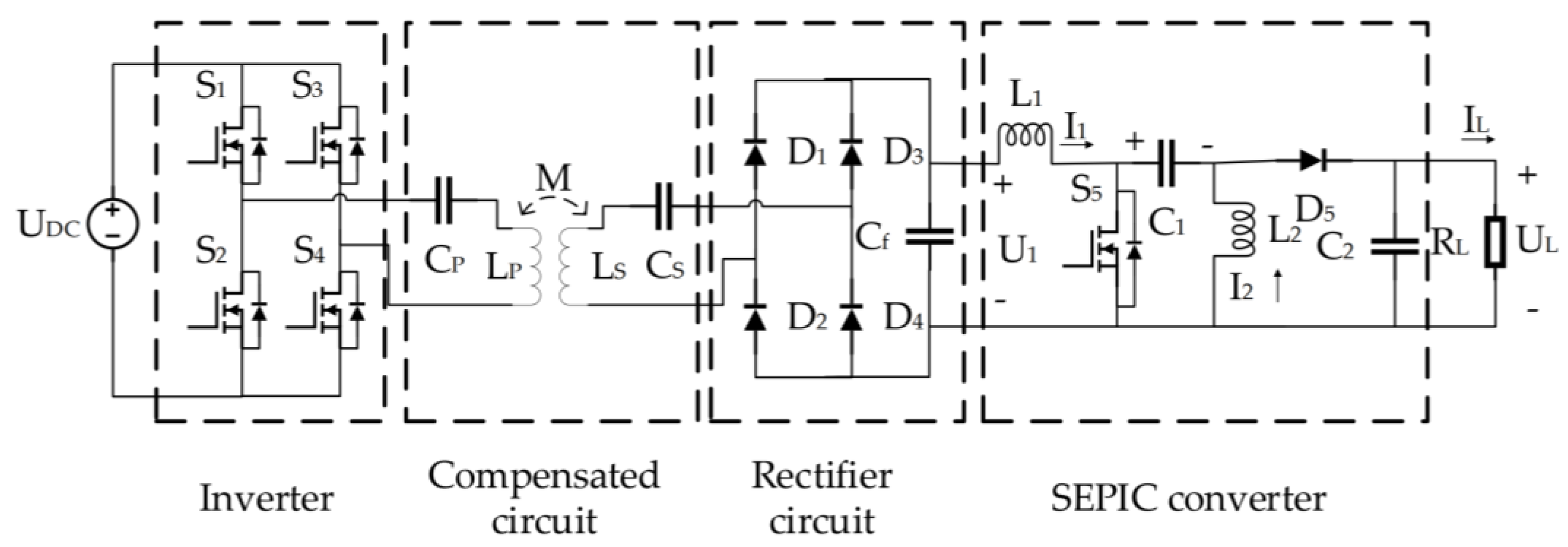
1.1. Overview of IPTS Architectures and Control Techniques

Figure 1 depicts one of the most commonly used architectures of the IPT systems based on the S–S compensation topology and using a full-bridge inverter on the transmitting (TX) side and a passive diode-bridge rectifier on the receiving (RX) side. The primary inverter converts the DC voltage and current waveforms of the source into the AC waveforms applied to the primary resonant tank, which is composed of a primary IPT coil and the respective resonant capacitor. The power is wirelessly transferred between the primary and the secondary coil by means of mutual coupling, and the resulting AC voltage and current waveforms of the secondary resonant tank are rectified by the diode-bridge and delivered to the load. For such IPTS topology, it is not possible to realize the output voltage regulation entirely on the RX side, since the diodes are automatically turned on and off depending on the secondary coil current direction. The research presented in [13] proposed a control scheme to regulate the output voltage of the S–S IPTS with passive rectification by controlling the switching frequency or the phase-shift angle of the full-bridge inverter. A detailed dynamic analysis based on the extended describing function technique was presented and the small-signal model of the system derived including both the frequency and the phase-shift control. However, such a control strategy requires the presence of a communication link between the TX and RX sides, which introduces a delay in the control loop and thus limits the dynamic performances of the proposed control scheme.
An active rectification scheme replaces rectifier diodes with power MOSFETs, thus allowing to control their switching process and directly regulate the output voltage on the RX side, without using any communication link with the TX side. In [14], a fixed-frequency phase-shift control strategy was proposed for dual active IPTS including full-bridge inverter and rectifier. In such a scheme, the secondary phase-shift angle is controlled to regulate the system output voltage, while the primary phase-shift angle is adjusted to achieve the minimum duty-cycle needed for zero-voltage switching (ZVS). The complication of the proposed scheme is that the current phase detection circuits are required on both the TX and RX sides to realize the proposed control strategy.
A similar bidirectional S–S IPTS with a double active bridge configuration was presented in [17], with the difference that two cascaded contactless transformers have been adopted for energy charging between electric vehicles. Two control strategies were implemented: the Primary Phase-Locked Loop (P-PLL) and Pulse-Width Modulation (PWM) control (P-PLL&PWM) and the Primary Constant Frequency plus Secondary PWM control (P-CF+S-PWM). In the P-PLL&PWM control scheme depicted in Figure 2, the PWM controller regulates the pulse width of the primary full-bridge inverter to regulate the output voltage, and the PLL control strategy regulates the frequency of the inverter to the achieve the ZVS of power devices on the primary side, while the active bridge rectifier on the RX side works as a conventional rectifier circuit. In the P-CF+S-PWM scheme shown in Figure 3, the primary inverter provides a full square-wave voltage having a constant switching frequency, while the output voltage regulation is realized entirely on the RX side by controlling the rectifier pulse-width duration. Hence, the second approach does not require a communication link between the TX and RX side. The experimental results suggest that the P-CF+S-PWM control has higher efficiency. However, such a strategy does not consider the efficiency maximization and can therefore be improved.
A more complex IPTS scheme with active rectification and a post-regulator on the RX side depicted in Figure 4 was proposed in [18] with the scope to maximize the efficiency as well as increase the amount of extractable power while operating in non-resonant conditions. The proposed method is based on actively modifying the equivalent secondary-side load impedance ZL seen at the rectifier input, by controlling the phase-shift φ of the active rectifier and its output voltage level Vr. This parameter can be controlled by either adjusting the duty-cycle D of the post-regulator or by varying the duty-cycle δ of the active rectifier, as shown in Figure 5. The phase-shift φ between the secondary voltage VL and current IL is realized by inserting a time delay between the primary and secondary side control signals, which is achieved by using a communication link between the primary and secondary side controllers. The proposed scheme considers a constant battery voltage at the IPTS output and does not perform the output voltage regulation, which could be a drawback for different types of load.
To enhance regulation capabilities of the IPTS schemes with passive rectification such as the one depicted in Figure 1, pre- or post-regulators can be adopted. Some of the papers introducing IPTSs with post-regulating DC/DC converters have used the perturb-and-observe (P&O) techniques to achieve maximum system efficiency. The research presented in [19] proposed the S–S IPTS using a passive diode-bridge rectifier followed by a cascaded boost-buck converter. A P&O technique was adopted which searches for the optimal post-regulator duty-cycle value maximizing the overall system efficiency obtained at the IPT resonant frequency. Similarly to the work presented in [18], no regulation of the output voltage was included in the above control scheme. In [20], a method for automatic maximum efficiency point tracking of the IPTS followed by a buck–boost converter was proposed. The presented algorithm searches for the minimum input power operating point for a given output power by varying the phase-shift of the inverter, while the PI controller of the buck–boost adjusts the output voltage. Because the searching process is carried out on the TX side, the proposal does not require any feedback from the RX side. The research in [21] proposes some improvements with respect to [20], by adopting a Discrete Sliding Mode Control (DSMC) scheme for the buck–boost post-regulator. The TX side of the adopted IPTS comprises a phase-shift full-bridge inverter, which incorporates the hill-climbing-search-based phase angle control for achieving minimum input current injection from its DC source, thereby attaining minimum the input power operation. The buck–boost converter realizes the output voltage regulation by means of the proposed DSMC scheme, which outperforms classical PI controller-based schemes in terms of better dynamic performances.
The S–S IPTS with a passive rectifier and a Single-Ended Primary Inductor Converter (SEPIC) depicted in Figure 6 was proposed in [22]. The SEPIC topology offers several benefits in switching power supplies thanks to its non-inverting step-up/step-down conversion ratio, to the possibility of reducing the size of magnetic components by using coupled inductors and to its loss-less resistor behavior in power factor pre-regulation applications [23]. A phase-shift control of the primary inverter was designed to regulate the primary coil current at a given reference value, in order to optimize the equivalent load resistance seen at the post-regulator input for maximum energy efficiency. A peak-current-control of the SEPIC was configured to guarantee the output voltage regulation under different load conditions. A disadvantage of the proposed approach consists of utilizing a refence value for the primary current (to achieve the optimal load conditions) which is very sensitive to the coupling coefficient and system component variations.
A more complicated control scheme for the IPTS with a passive rectification and a buck–boost post-regulator was proposed in [24] with the aim of maximizing the overall system efficiency while maintaining a constant output power level. In such a scheme, a primary-to-secondary voltage ratio is regulated through the buck–boost duty-cycle control to reach the maximum efficiency under resonance conditions, while the IPTS input voltage is adjusted to yield the target output power to the load. Such a control scheme requires a pre-regulator (e.g., a boost converter) to change the IPTS input voltage, which ends up being complicated for practical implementations; moreover, the proposed voltage ratio control criterion is only valid under given resonance conditions. Finally, the output voltage regulation is not included in the above control scheme.
The authors in [25] presented a Maximum Efficiency Point (MEP) tracking method for IPTSs whose RX side contains either a passive rectifier with post-regulator or a regulating rectifier. This last rectification topology uses two additional MOSFETs at the input of the diode bridge which are periodically turned on and off to regulate the IPTS output voltage. It is proven that, under resonance conditions, at the MEP, the derivative of post-regulator duty-cycle D with respect to the inverter DC input voltage Vin is equal to or smaller than a constant β determined by the system parameters, namely dD/dVinβ. It is also shown that increasing Vin allows to reach the MEP as soon as dD/dVin becomes equal to or lower than β. Thus, the MEP can be tracked without a power or current sensor.
Four different IPTS schemes and relative control techniques were analyzed and compared in [16], with the scope to achieve the output voltage regulation: Lower-side Frequency Control (LFC), Higher-side Frequency Control (HFC), pre-regulation, and post-regulation. The first two techniques are based on the behavior of an open-loop IPTS which presents two peaks near the split frequencies in the “over coupled” region, as depicted in Figure 7. In particular, LFC (HFC) controls the inverter switching frequency on the left (right) side of the low (high) split frequency to regulate the IPTS output voltage. Conversely, the pre- (post-) regulation scheme adopts a DC/DC converter on the primary (secondary) IPT side to regulate the output voltage by fixing the switching frequency and controlling the converter duty-cycle. A Maximum Efficiency Point Tracking (MEPT) control scheme was proposed based on the use of a both pre- and post-regulating DC/DC converter (see Figure 8), where the output voltage regulation is accomplished by the post-regulator controller, while the maximum efficiency is achieved by the pre-regulator controller.
Eventually, Ref. [26] presented an MEPT algorithm for the post-regulated IPTS to match the load impedance to that of the source impedance. The proposed algorithm varies both the switching frequency and the phase-shift of the inverter to minimize the input power, whereas the output power is kept constant by a buck converter, which is used to regulate the battery voltage and current. The drawback of the proposed study is that, during the buck controller design, the influence of the IPTS on the duty-to-output transfer function of the buck converter is not taken into account.
In this paper, we overcome such a limitation by correctly modeling the post-regulator dynamics accounting for the IPTS connected to its input. To this end, we exploit the findings of [27] which used Coupled-Mode Theory (CMT) to deal with the dynamic modeling of the IPTS pre-regulated by a buck converter. Such an approach uses slowly varying amplitudes and phases of coupled modes, rather than resonant currents and voltages, to model the coupled resonances of the IPT stage. It also includes the non-linearities of the inverter and rectifier stages operating at a full square-wave voltage under IPTS resonant conditions. A continuation of [27] can be found in [28], where the steady-state and dynamic characteristics of an open-loop IPTS post-regulated by a buck–boost converter are investigated by means of the CMT. It is shown that, for certain operating conditions and system component values, the steady-state control-to-output curve of the post-regulator can be non-monotonic, since its static and dynamic characteristics are tightly coupled to the IPT stage. In particular, when the control-to-output curve changes its slope and starts decreasing, the system runs into positive feedback and goes out of control. In this paper, we enhance the modeling procedure proposed in [27,28] by including the inverter phase-shift modulation and by extending its validity to whatever operating frequency. Such an enhanced procedure is herein formulated for the buck post-regulator, but its findings are general and can also be applied to other basic converter topologies (e.g., boost, buck–boost, etc.).
A comparison between the main IPTS solutions discussed previously and the system developed in this work is subsequently provided in the Section 4.4, highlighting their relevant features and specifications.

2. Static Modeling of Post-Regulated IPTS

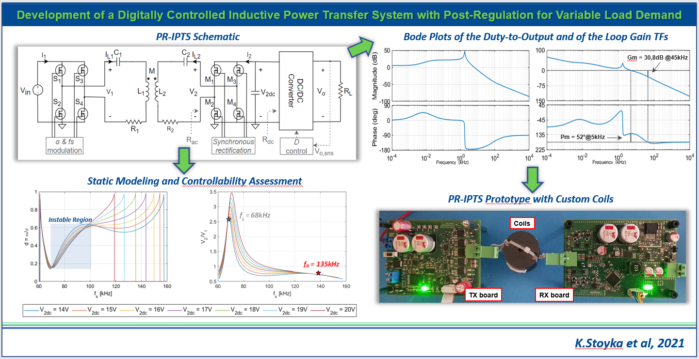
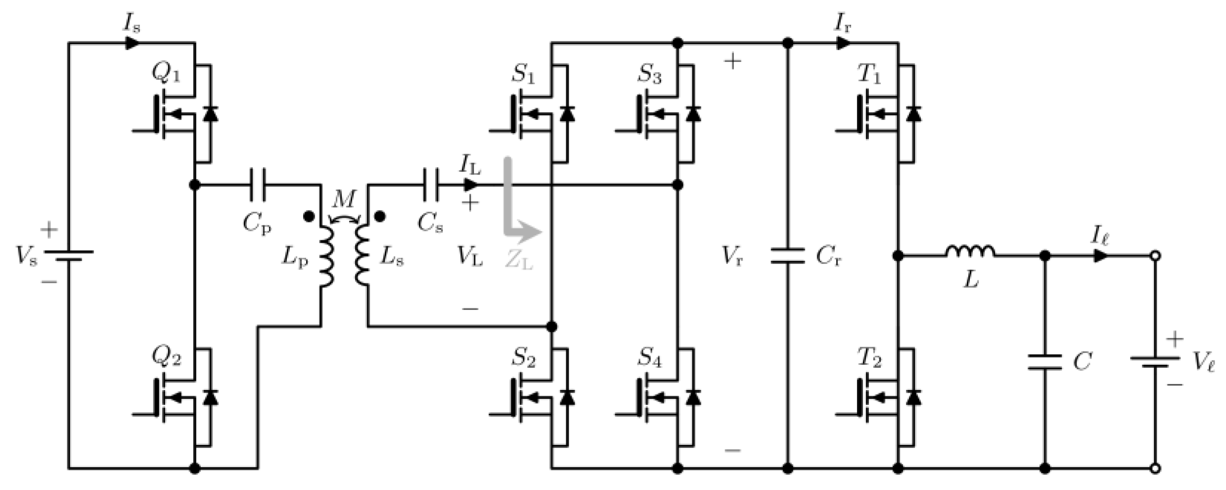
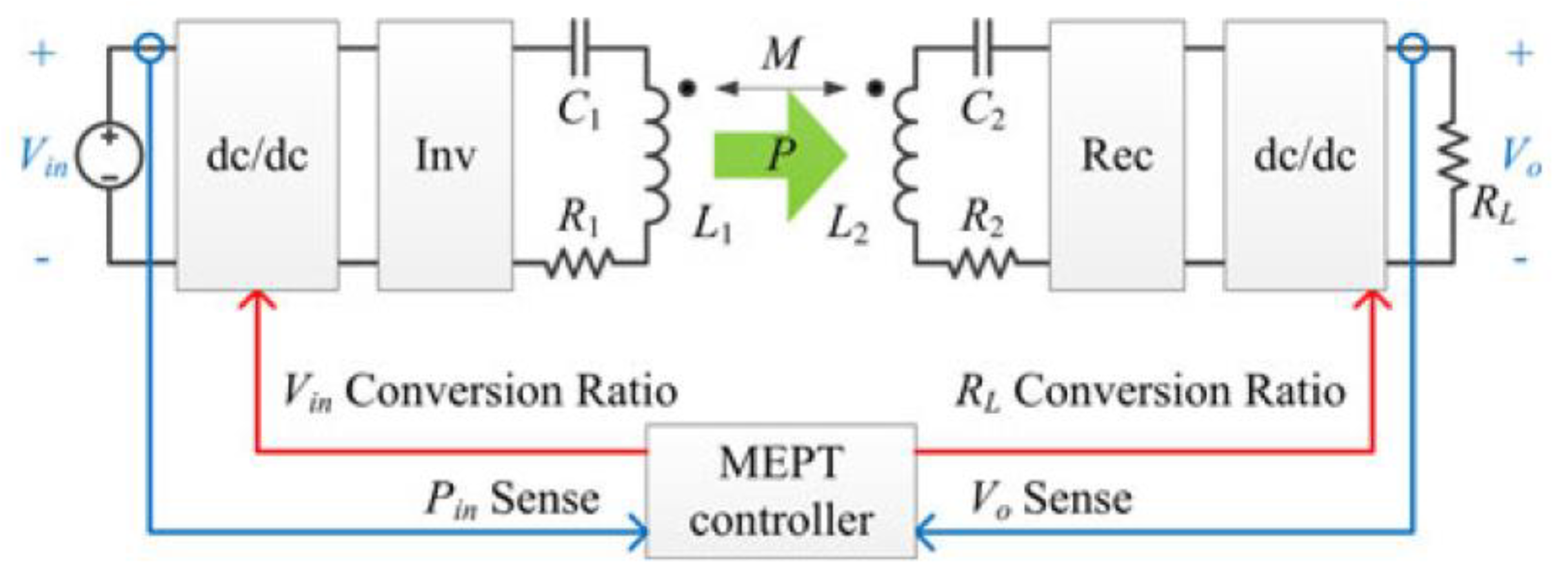
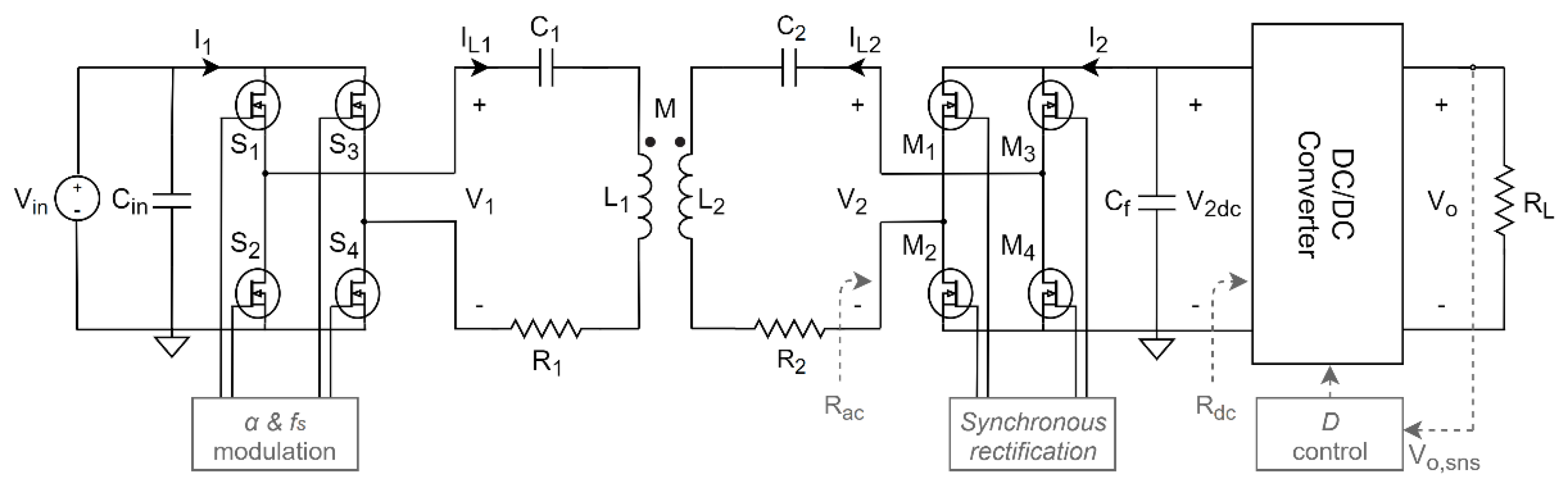
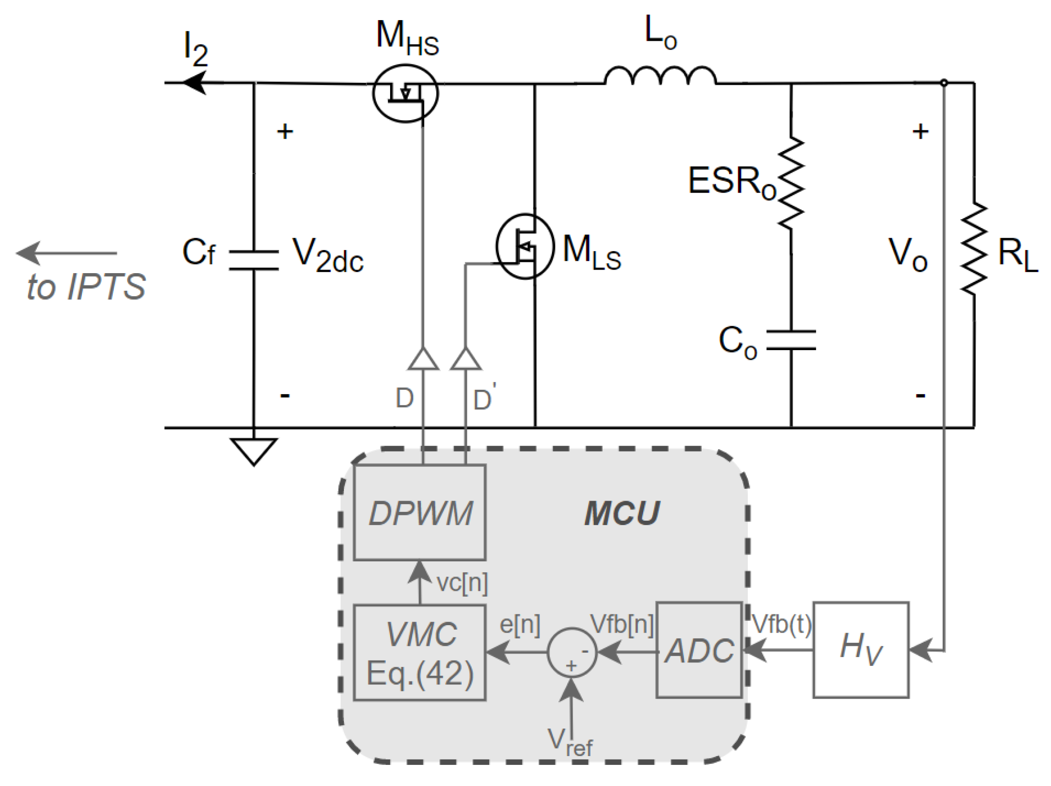
2.1. Post-Regulated IPTS (PR-IPTS)

Figure 9 shows a schematic of a Post-Regulated IPTS (PR-IPTS) using a series–series compensation topology. The coupling coils, represented by the self-inductances L1 and L2, are compensated with the series capacitors C1 and C2. The magnetic coupling between the coils is represented by their mutual inductance M. The TX coil is connected to the source through a MOSFET full-bridge inverter implementing a phase-shift and frequency modulation, with the objective of maximizing the overall system efficiency. The phase-shift modulation consists of modulating the phase angle α between the complementary square-wave gate signal pairs used to control the MOSFETs of the two inverter legs, as depicted in Figure 10. As a result, a modified square-wave voltage v1(t) is obtained at the inverter output (indicated by the green waveform in Figure 10). The resistor R1 includes the equivalent resistances of L1, C1 and of the two inverter MOSFETs conducting simultaneously.
The RX coil is connected to the resistive load RL through a MOSFET full-bridge rectifier followed by a buck DC/DC converter implementing a duty-cycle D control at a fixed switching frequency fBuck. Such control aims to regulate the system output voltage Vo at a desired nominal value Vo,nom, under both static and dynamic load conditions. As a result of the presence of the buck converter, the equivalent DC resistance seen at the rectifier output is given by (1):
R d c = R L / M ( D ) 2
where M(D) = Vo/V2dc = D represents the buck conversion ratio while V2dc is the intermediate bus voltage between the rectifier and the buck. The resistor R2 includes the equivalent resistances of L2, C2 and of the two rectifier MOSFETs conducting simultaneously. A synchronous rectification scheme has been herein adopted for the full-bridge rectifier, in which each MOSFET is turned on after a short conduction of the relative body-diode (as soon as its drain–source voltage decreases below a given negative threshold), and is turned off when its drain–source voltage exceeds the threshold [29]. Thus, the conduction losses can be reduced as compared to the passive diode bridge configuration [30].

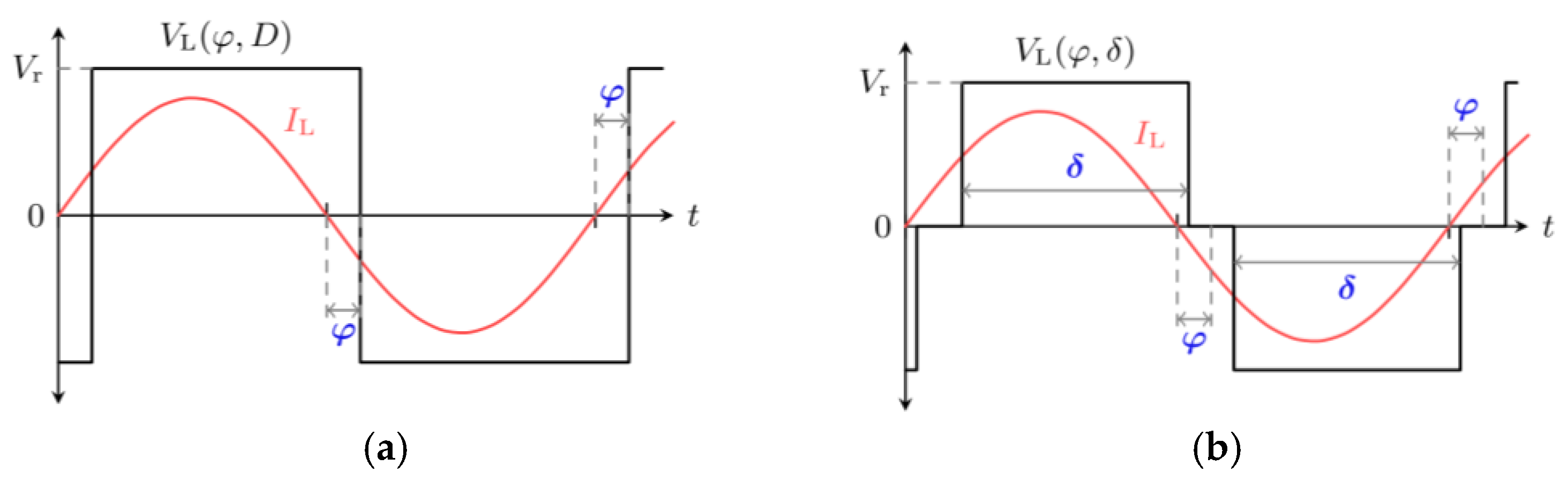
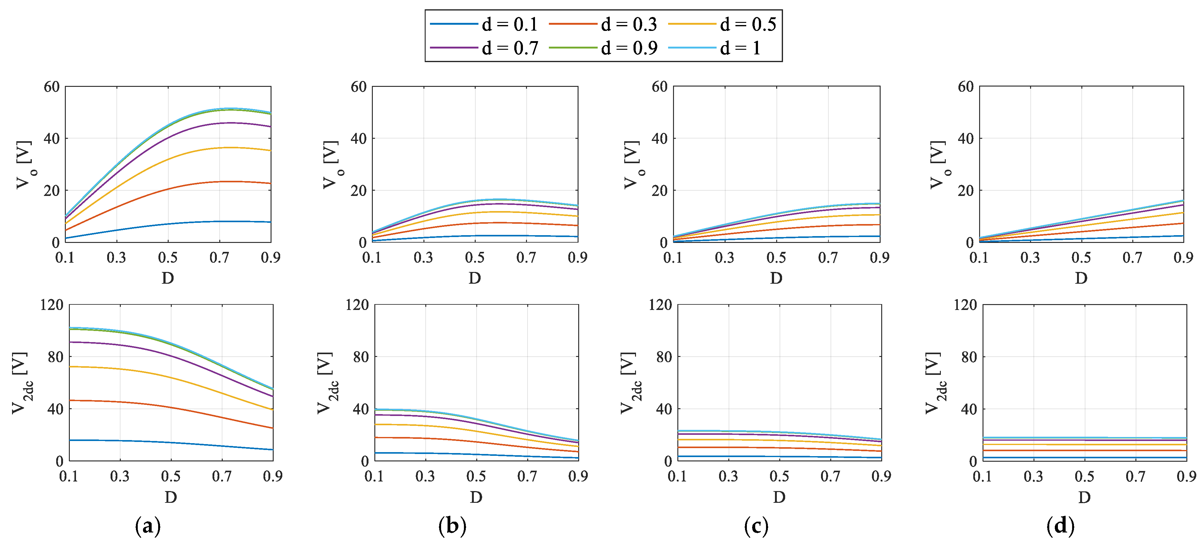
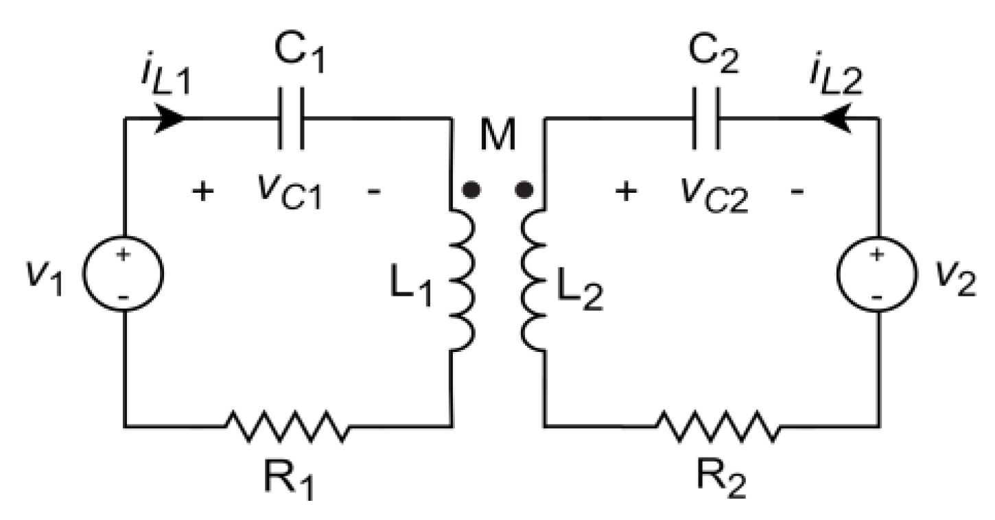
2.2. Static Modeling of PR-IPTS

The above PR-IPTS has been modeled using an FHA method, since the primary and the secondary coil currents are nearly sinusoidal, and only the first harmonics of the voltages (v1(t), v2(t)) and currents (iL1(t), iL2(t)) contribute to the power transfer. Such FHA quantities can be represented through their respective phasors V ¯ 1 = V 1 e j ϕ V 1 , V ¯ 2 = V 2 e j ϕ V 2 , I ¯ L 1 = I L 1 e j ϕ L 1 , I ¯ L 2 = I L 2 e j ϕ L 2 .
As a result of the phase-shift modulation, the peak amplitude of the primary voltage phasor is given by (2):
V 1 = 4 π V i n sin ( α 2 )
The FHA allows to model the power electronics connected to the RX side with an equivalent AC resistance Rac, expressed as the ratio between the amplitudes of the first harmonics of voltage and current at the input of the rectifier bridge [1]:
R a c = V 2 I L 2 = 8 π 2 R d c
Under FHA assumption, the analyzed IPTS can be described with the following phasor equation system (4):
{ V ¯ 1 = ( j ω s L 1 + 1 j ω s C 1 + R 1 ) I ¯ L 1 + j ω s M I ¯ L 2 V ¯ 2 = j ω s M I ¯ L 1 + ( j ω s L 2 + 1 j ω s C 2 + R 2 ) I ¯ L 2 = R a c I ¯ L 2
where ωs = 2πfs represents the angular switching frequency of the inverter. For a certain value of the intermediate bus voltage V2dc, the equivalent resistance Rac, seen by the IPT secondary side, can be evaluated using (1) and (3), while the peak amplitude of the secondary voltage first harmonic is given by (5):
V 2 = 4 π V 2 d c
If the phase ϕV2 is taken as a zero reference for the phase angles, the phasor V ¯ 2 = V 2 is known, and the equation system (4) can be solved to obtain the remaining phasors, as given in (6):
I ¯ L 2 = V ¯ 2 R a c   ,             I ¯ L 1 = ( j ω s L 2 + 1 j ω s C 2 + R 2 + R a c ) j ω s M V ¯ 2 R a c V ¯ 1 = [ ( j ω s L 1 + 1 j ω s C 1 + R 1 ) ( j ω s L 2 + 1 j ω s C 2 + R 2 + R a c ) + ω s 2 M 2 ] j ω s M V ¯ 2 R a c
Starting from (6), it is possible to evaluate the peak amplitude of the primary voltage first harmonic V1, and estimate the resulting phase-shift α by inverting (2):
α = 2 arcsin ( π 4 V 1 V i n )
If the resulting α value is real and included in the range [0, π], the analyzed operating condition (relative to the considered V2dc value) is feasible, and the primary and secondary IPT average powers P1 and P2 can be evaluated according to (8):
P 1 = 1 / 2   R e { V ¯ 1 I ¯ L 1 * } P 2 = 1 / 2   R e { V ¯ 2 I ¯ L 2 * }
Note that such average powers do not take into account the inverter switching losses, the coils ferrite core losses and the post-regulator losses, since simplified FHA modeling do not allow for including such loss contributions. However, the above approach does enable the evaluation of the overall system behavior under different operating conditions of fs and V2dc, which are the two main parameters used herein to optimize the IPTS efficiency η = P2/P1.

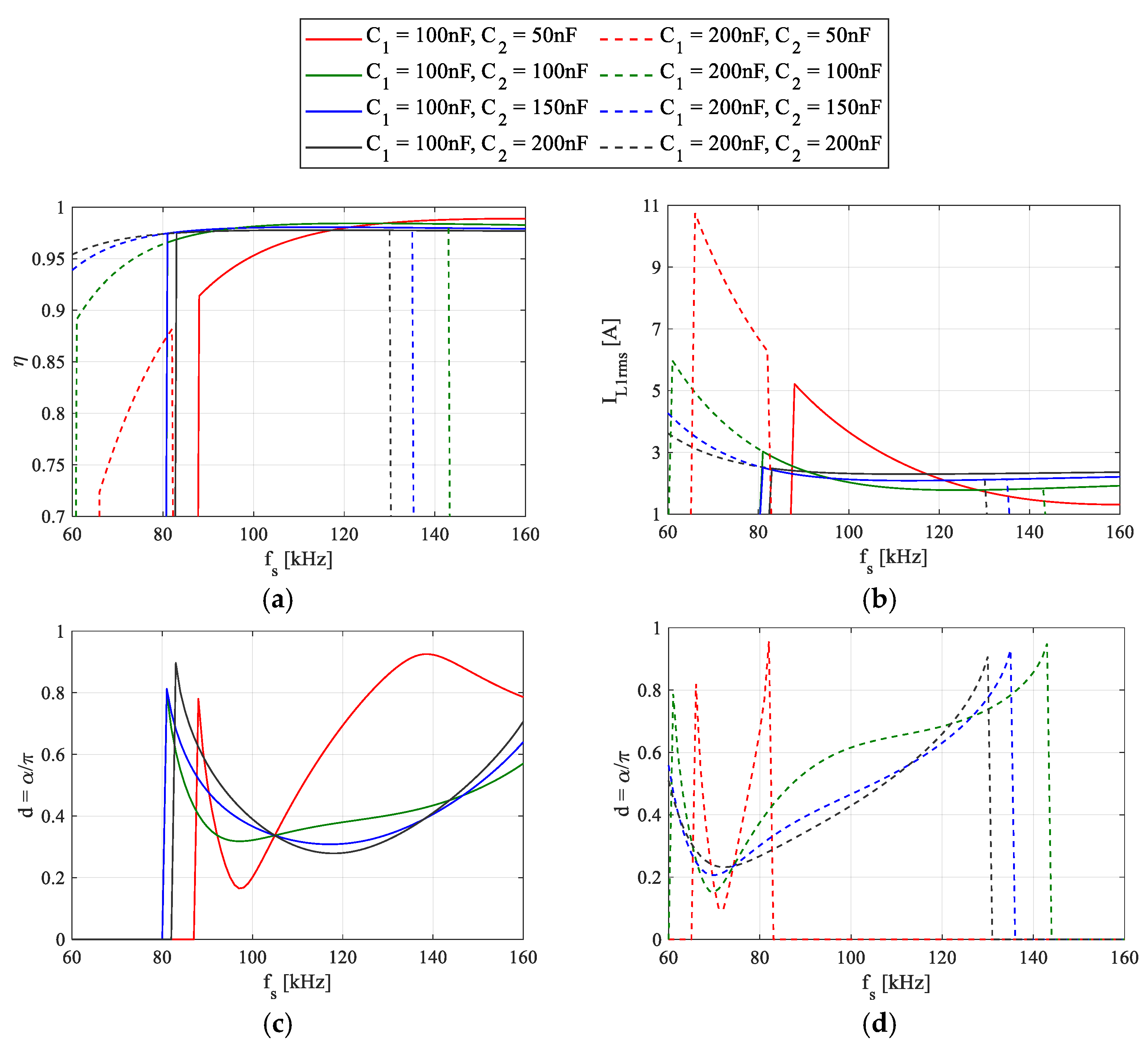
2.3. Compensation Capacitors Selection

For a given TX and RX coil set, the IPTS power and efficiency levels depend on the selected values of the compensation capacitors C1 and C2, as highlighted by the IPTS modeling solution (5)–(8). Given the IPTS operating parameters and component values listed in Table 1, Equations (5)–(8) have been evaluated for V2dc = 17 V, C1 = {100, 200} nF and C2 = {50, 100, 150, 200} nF. The IPT coil design resulting in the coil parameters of Table 1 will be subsequently described. Note that the analyzed IPTS has been herein designed to deliver an average output power of approximately 20 W at a regulated output voltage of 12 V to a resistive load of 7 Ω, but different output power levels are also feasible and will be tested in the experimental section of this paper. Figure 11 depicts the simulated IPTS efficiency η (Figure 11a), the primary coil rms current IL1rms = I L 1 / 2 (Figure 11b), and the normalized phase-shift d = α/π (Figure 11c,d)), for C1 = 100 nF (solid lines) and C1 = 200 nF (dashed lines). Note that only the TX coil rms current is shown in Figure 11b, since the RX coil current does not depend on the C1, C2 and fs values. The plots of Figure 11c,d highlight the fact that the phase-shift changes with both C1 and C2, since it is dependent on the V ¯ 1 solution in (6). The points with d = 0 represent unfeasible operating conditions for which the output voltage regulation cannot be achieved. The plots of Figure 11a,b show that η and I1rms levels only depend on C2, while C1 determines the operating ranges wherein the IPTS modeling solution is feasible (α ∈ [0, π] or d ∈ [0, 1]). The capacitor values C1 = 100 nF and C2 = 50 nF enable achieving the highest simulated efficiency (red solid curve in Figure 11a) at high frequencies, where the converters switching losses and the coils ferrite losses are likely to become high. For this reason, the optimal choice is C2 = 100 nF (green curve) allowing to maximize the efficiency at ~120 kHz, with both C1 = 100 nF and 200 nF.

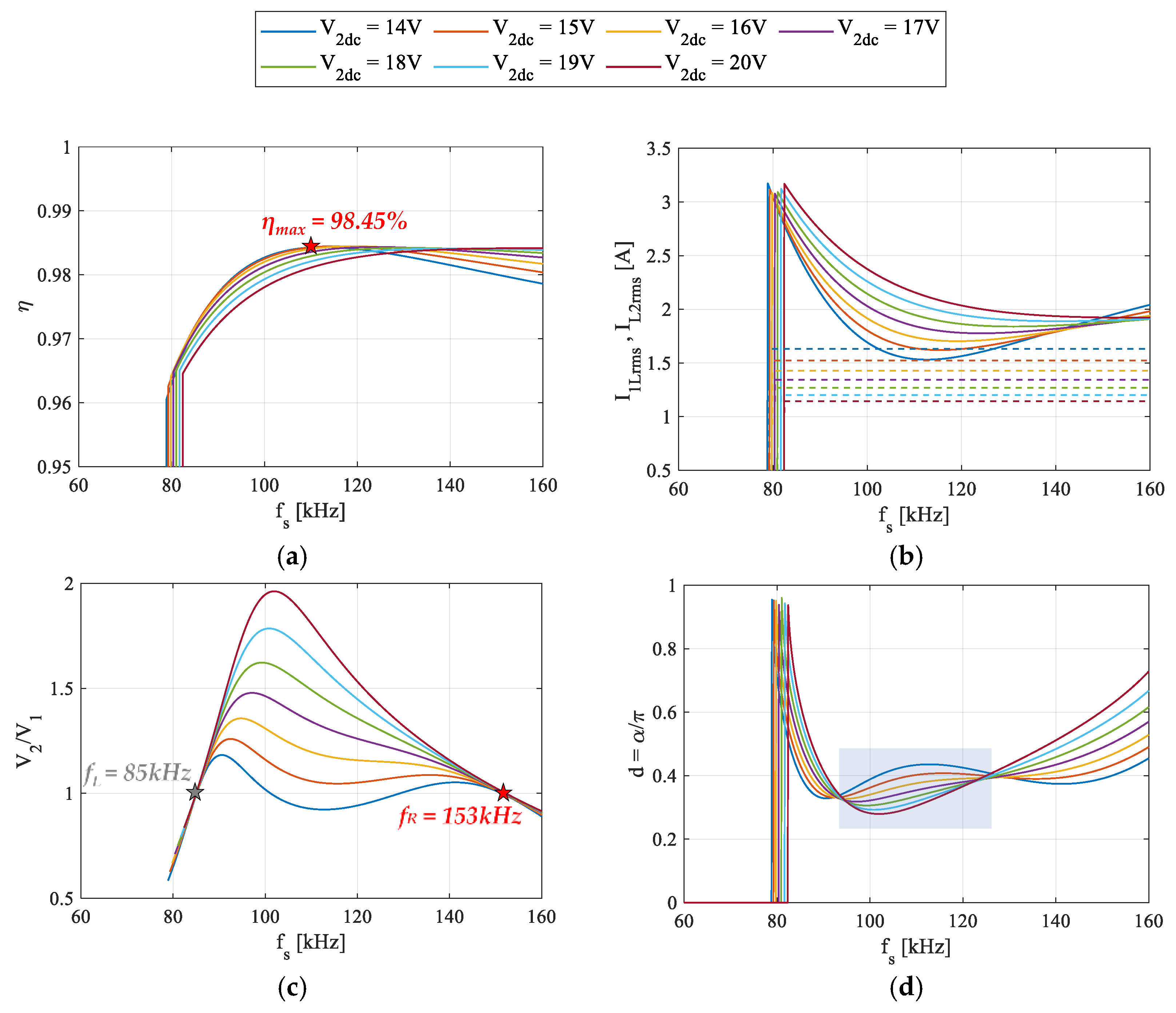
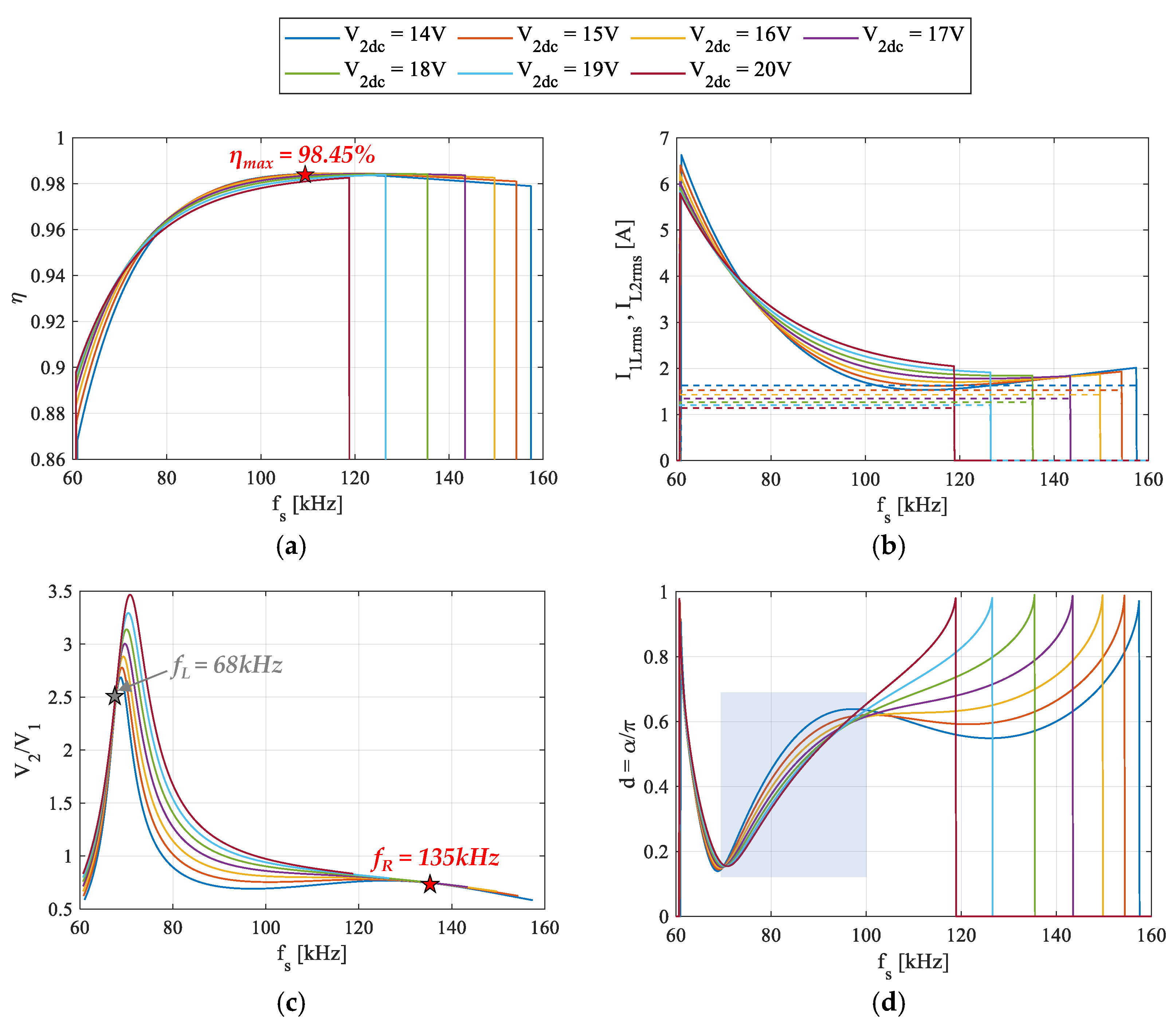
2.4. Static Modeling Results

Once the optimal compensation capacitor values have been selected, the IPTS modeling solution (5)–(8) has been evaluated over the ranges V2dc = [14, 20] V and fs = [60, 160] kHz, in order to determine the optimal parameter values maximizing the overall IPTS efficiency. Note that, in practice, a certain value of V2dc can be achieved through the inverter phase-shift modulation (for a given value of fs), either in an open-loop fashion or through the closed-loop feedback control. However, the latter would require a communication link between the IPT primary and secondary side; therefore, the open-loop strategy has been adopted herein.
Two different capacitor set-ups, identified as the optimal ones in the previous sub-section, have been analyzed and compared: {C1 = 100 nF, C2 = 100 nF} and {C1 = 200 nF, C2 = 100 nF}. Figure 12 depicts the simulated IPTS efficiency η (Figure 12a), the rms currents IL1rms (solid lines) and IL2rms (dashed lines) of the TX and RX coil, respectively (Figure 12b), the IPT stage voltage gain V2/V1 (Figure 12c) and the normalized phase-shift d (Figure 12d), for the first capacitor set-up {C1 = 100 nF, C2 = 100 nF}. The plot of Figure 12a highlights that, for different frequencies, the simulated efficiency can be maximized at different levels of V2dc (different line colors in the plots). For this set-up, the maximum value ηmax = 0.9845 has been obtained at V2dc = 15 V and fs = 115 kHz. Figure 12b shows that the secondary coil rms current level (dashed lines) does not depend on the frequency, since it only depends on V2dc and Rac values, as described by (6). Figure 12c highlights the fact that the IPTS voltage gain is independent of V2dc (and hence of Rac) at two split frequencies [28]:
f L = 1 2 π 1 k 2 ω 1 2 + ω 2 2 2 ( ω 1 2 ω 2 2 2 ) 2 + ω 1 2 ω 2 2 k 2 f R = 1 2 π 1 k 2 ω 1 2 + ω 2 2 2 + ( ω 1 2 ω 2 2 2 ) 2 + ω 1 2 ω 2 2 k 2
where ω1 = 2πf1 = 1/ L 1 C 1 and ω2 = 2πf2 = 1 / L 2 C 2 are the primary and the secondary side angular resonant frequencies. For the capacitor set-up of Figure 12, the split frequencies are located in fL = 85 kHz and fR = 153 kHz. As will be explained in the next section, operating at the right-side split frequency fR can be beneficial in terms of better controllability of the post-regulated IPTS, while maintaining high efficiency due to the ZVS inverter operation [31]. Finally, the blue rectangle in Figure 12d highlights a frequency region (from approximately 95 kHz to approximately 125 kHz) wherein the V2dc voltage decreases as the normalized phase-shift d increases. This behavior could determine an instable operation region for the buck controller wherein the regulation of the buck output voltage could be lost, as will be explained hereafter. Hence, it could be impossible to exploit the maximum efficiency over such a frequency range, while operating the IPTS at higher frequencies could lead to decreased efficiency due to the increasing switching and ferrite losses.
Figure 13 depicts the simulated IPTS efficiency η (Figure 13a), the rms currents IL1rms (solid lines) and the IL2rms (dashed lines) of the TX and RX coils, respectively (Figure 13b), the IPTS voltage gain V2/V1 (Figure 13c) and the normalized phase-shift d (Figure 13d), for the second capacitor set-up {C1 = 200 nF, C2 = 100 nF}. Also for this configuration, the maximum value ηmax = 0.9845 has been obtained at V2dc = 15 V and fs = 115 kHz, since C1 does not influence the maximum efficiency but the feasible frequency range over which such efficiency can be obtained. The split frequencies, for which the IPTS voltage gain is independent of the load, are now located in fL = 68 kHz and fR = 135 kHz. Again, the blue rectangle in Figure 13d highlights a frequency region (from approximately 70 kHz to approximately 100 kHz), wherein the V2dc voltage decreases as the normalized phase-shift d increases, over which the buck controller could lose the capability of regulating the output voltage, as explained in the following section. However, compared to the capacitor set-up of Figure 12, now such a critical frequency region is shifted to the left, thus allowing to exploit the maximum efficiency operating conditions around the fs = 115 kHz point. Hence, the optimal compensation capacitor set-up selected herein is {C1 = 200 nF, C2 = 100 nF}, resulting in the following values of the primary and secondary resonant frequencies f1 = 74 kHz and f2 = 105 kHz.

2.5. PR-IPTS Controllability Assessment

The modeling results presented in the previous section are based on the assumption that the buck converter correctly regulates its output voltage for all the analyzed conditions of the inverter switching frequency fs and the intermediate bus voltage V2dc. However, the control characteristics of a post-regulator cascaded to an IPTS are quite different from a standalone DC/DC converter [28]. This is due to the fact that, as the post-regulator duty-cycle D increases, the equivalent resistance Rac seen by the IPT stage decreases, and the intermediate bus voltage V2dc can either increase or decrease in function of the IPTS response to the equivalent load variation. Hence, the converter output voltage Vo = V2dc·M(D) can increase or decrease with the duty-cycle, in function of the amount of V2dc· and M(D) variation with D. Under certain operating conditions, the output voltage can become non-monotonic with respect to the duty-cycle, which means that the resulting Bode diagram varies significantly with the operating point. This may lead to difficulties in closed-loop control. In this section, we solve the PR-IPTS equations with the buck converter operating in open-loop and show that the non-monotonic behavior of the output voltage with duty-cycle occurs within the operating regions highlighted with blue rectangles in Figure 12d and Figure 13d.
Let us assume that the PR-IPTS is operating in open loop with the buck duty-cycle varying in the range D = [0.1, 0.9]. The system equation (4) is still valid, but the output voltage Vo is no more regulated at its nominal value. The equivalent AC resistance Rac seen at the rectifier input changes with the duty-cycle according to (1) and (3), thus varying the IPTS operating point. Let us also assume that the inverter normalized phase-shift d is varied in the range d = [0.1, 1]. For each value of d, the primary voltage peak V1 is given by (2) and, if the phase ϕV1 is taken as a zero reference for the phase angles, the phasor V ¯ 1 = V 1 is known, and the equation system (4) can be solved to obtain the remaining phasors, as given in (10):
I ¯ L 1 = ( j ω s L 2 + 1 j ω s C 2 + R 2 + R a c ) ( j ω s L 1 + 1 j ω s C 1 + R 1 ) ( j ω s L 2 + 1 j ω s C 2 + R 2 + R a c ) + ω s 2 M 2 V ¯ 1 I ¯ L 2 = j ω M ( j ω s L 1 + 1 j ω s C 1 + R 1 ) ( j ω s L 2 + 1 j ω s C 2 + R 2 + R a c ) + ω s 2 M 2 V ¯ 1 V ¯ 2 = j ω M R a c ( j ω s L 1 + 1 j ω s C 1 + R 1 ) ( j ω s L 2 + 1 j ω s C 2 + R 2 + R a c ) + ω s 2 M 2 V ¯ 1
Starting from the result of (10), the voltage V2dc can be estimated by inverting (5), and the resulting output voltage can be obtained for each analyzed value of D as Vo = V2dc·D. Figure 14 shows the values of Vo and V2dc for the capacitor set-up {C1 = 200 nF, C2 = 100 nF}, obtained over the given ranges of D and d for fs values in the interval [70, 135] kHz. It can be observed that at fs = 70 kHz (Figure 14a), Vo is non-monotonic with respect to D, while V2dc reaches very high levels for low duty-cycle values (high Rac). Such a condition could result in an unstable controller behavior within the positive feedback region located at the right-hand-side of the Vo vs. D curve peak. In this region, an increase in D would result in a decrease in Vo, and the controller would try to further increase D until saturating its value at the maximum allowed limit. Hence, the output voltage regulation would be lost. Similarly, a decrease in D would cause an increase in Vo, and the controller would try to further decrease the duty-cycle, until reaching the Vo vs. D curve peak and going to the negative feedback region. In principle, in such a region the controller could be able to guarantee the output voltage regulation, but V2dc may increase to very high levels, causing possible component failures (such as capacitors, buck converter MOSFETs and relative gate drivers, etc.). Hence, the system operation under conditions resulting in a non-monotonic control-to-output characteristic should be avoided. At fs = 90 kHz (Figure 14b), Vo is still non-monotonic with respect to D but V2dc assumes lower values, while at fs = 110 kHz (Figure 14c), Vo becomes monotonic resulting in a correct controller behavior. These findings are in agreement with the results of Figure 13d, where the IPTS operation in the range [70, 100] kHz is not recommended because of the inversion of the V2dc vs. d trend. Eventually, the plots of Figure 14d depict Vo and V2dc for fs = 135 kHz (corresponding to the right-hand-side split frequency fR), highlighting that V2dc (and consequently, the IPTS gain V2/V1) is independent of the duty-cycle D (or, equivalently, of Rac), which is in agreement with the results of Figure 13c. Hence, operating IPTS at fR can be convenient if the load variations occur, but the overall system efficiency may decrease somewhat (as can be seen in Figure 13a). To maximize the efficiency, IPTS should be operated at fs = 115 kHz, which is still a feasible condition located in the stable frequency region, as previously shown in Figure 13d.

3. Dynamic Modeling and Control of PR-IPTS

In this section, we describe the dynamic modeling of the PR-IPTS based on CMT, similarly to the research developed in [27]. In contrast to the findings of [27], which are valid for a full square-wave inverter operation under resonance conditions, we propose the modified modeling including the inverter phase-shift modulation which is valid for whatever switching frequency. As one of the modeling outputs, we obtained the duty-to-output transfer function of the post-regulator, necessary for the design of the digital controller as discussed hereafter.

3.1. Dynamic Modeling of IPT Stage

Figure 15 shows the AC equivalent circuit of the IPT stage of Figure 9, where v1 and v2 are considered to be the exciting source and sink, respectively. The dynamics of such an equivalent circuit can be described by the equation system (11):
{ L 1 d i L 1 d t + M d i L 2 d t + R 1 i L 1 + v C 1 = v 1 L 2 d i L 2 d t + M d i L 1 d t + R 2 i L 2 + v C 2 = v 2 C 1 d v C 1 d t = i L 1 C 2 d v C 2 d t = i L 2
As a result of the phase-shift modulation (see Figure 10), the inverter output voltage v1(t) can be described by (12):
v 1 ( t ) = { v i n   ,         α 2 ω s t < α 2                           0 ,                         α 2 ω s t < π α 2       v i n ,       π α 2 ω s t < π + α 2  
The rectifier input voltage v2(t) is determined by the secondary coil current direction:
v 2 ( t ) = s g n ( i L 2 ( t ) ) v 2 d c
According to the CMT, the IPT coil currents iLn(t) and the compensation capacitor voltages vCn(t) (n = 1, 2) can be represented as given in (14):
{ i L n ( t ) = 2 L n a n cos ( ω s t + θ n ) ( 14 a ) v C n ( t ) = 1 ω s C n 2 L n a n sin ( ω s t + θ n ) ( 14 b )
where an and θn are the amplitudes and phases of the coupled modes representing the state of the primary and secondary resonators. Such variables are assumed to vary slowly with time. Let us note that (14b) has been modified compared to the formulation given in [27], so as to extend its validity to whatever operating frequency. Using (14), the derivatives of the resonant voltages and currents become:
{ d i L n d t = 2 L n [ d a n d t cos ( ω s t + θ n ) a n ( ω s + d θ n d t ) s i n ( ω s t + θ n ) ] d v C n d t = 2 C n [ d a n d t sin ( ω s t + θ n ) + a n ( ω s + d θ n d t ) c o s ( ω s t + θ n ) ]
By substituting (15) into (11), it is possible to derive the dynamic equations of the amplitudes and phases of the coupled modes:
d a 1 d t = ω 1 a 1 s i n ( ω s t + θ 1 ) c o s ( ω s t + θ 1 ) + + L 1 / 2 ( L 1 L 2 M 2 ) cos ( ω s t + θ 1 ) [ L 2 ω s C 1 2 L 1 a 1 s i n ( ω s t + θ 1 ) + L 2 R 1 2 L 1 a 1 c o s ( ω s t + θ 1 ) + L 2 v 1 ( t ) M v 2 ( t ) + + M R 2 2 L 2 a 2 c o s ( ω s t + θ 2 ) + M ω s C 2 2 L 2 a 2 s i n ( ω s t + θ 2 ) ]
d θ 1 d t = ω s + ω 1 ω 1 sin 2 ( ω s t + θ 1 ) + L 1 / 2 ( L 1 L 2 M 2 ) s i n ( ω s t + θ 1 ) a 1 [ L 2 ω s C 1 2 L 1 a 1 s i n ( ω s t + θ 1 ) + L 2 R 1 2 L 1 a 1 c o s ( ω s t + θ 1 ) + L 2 v 1 ( t ) M v 2 ( t ) + + M R 2 2 L 2 a 2 c o s ( ω s t + θ 2 ) + M ω s C 2 2 L 2 a 2 s i n ( ω s t + θ 2 ) ]
d a 2 d t = ω 2 a 2 s i n ( ω s t + θ 2 ) c o s ( ω s t + θ 2 ) + + L 2 / 2 ( L 1 L 2 M 2 ) cos ( ω s t + θ 2 ) [ L 1 ω s C 2 2 L 2 a 2 s i n ( ω s t + θ 2 ) + + L 1 v 2 ( t ) M v 1 ( t ) + + M R 1 2 L 1 a 1 c o s ( ω s t + θ 1 ) + M ω s C 1 2 L 1 a 1 s i n ( ω s t + θ 1 ) ]
d θ 2 d t = ω s + ω 2 ω 2 sin 2 ( ω s t + θ 2 ) + L 2 / 2 ( L 1 L 2 M 2 ) sin ( ω s t + θ 2 ) a 2   [ L 1 ω s C 2 2 L 2 a 2 s i n ( ω s t + θ 2 ) + L 1 R 2 2 L 2 a 2 c o s ( ω s t + θ 2 ) + L 1 v 2 ( t ) M v 1 ( t ) + + M R 1 2 L 1 a 1 c o s ( ω s t + θ 1 ) + M ω s C 1 2 L 1 a 1 s i n ( ω s t + θ 1 ) ]
Note that (12) and (13) should be used in (16) to describe v1(t) and v2(t), respectively. Assuming that the slowly varying variables in (16)—an and θn (n = 1, 2)—are constant during a buck switching period TBuck = 1/fBuck, the time-invariant averaged model can be obtained by taking the average values of both sides of (16) over TBuck:
d a 1 d t = L 1 / 2 ( L 1 L 2 M 2 ) [ L 2 R 1 2 L 1 a 1 M ω s C 2 2 L 2 a 2 s i n ( θ 1 θ 2 ) + + M R 2 2 L 2 a 2 c o s ( θ 1 θ 2 ) + 2 L 2 v i n π cos ( θ 1 ) sin ( α 2 ) + 2 M π v 2 d c cos ( θ 1 θ 2 ) ]
d θ 1 d t = ω s + ω 1 2 L 1 / 2 ( L 1 L 2 M 2 ) a 1 [ L 2 ω s C 1 2 L 1 a 1 + M ω s C 2 2 L 2 a 2 cos ( θ 1 θ 2 ) + + M R 2 2 L 2 a 2 sin ( θ 1 θ 2 ) + 2 L 2 v i n π sin ( θ 1 ) sin ( α 2 ) + 2 M π v 2 d c sin ( θ 1 θ 2 ) ]
d a 2 d t = L 2 / 2 ( L 1 L 2 M 2 ) [ L 1 R 2 2 L 2 a 2 + M ω s C 1 2 L 1 a 1 s i n ( θ 1 θ 2 ) + + M R 1 2 L 1 a 1 c o s ( θ 1 θ 2 ) 2 L 1 v 2 d c π 2 M v i n π cos ( θ 2 ) sin ( α 2 ) ]
d θ 2 d t = ω s + ω 2 2 L 2 / 2 ( L 1 L 2 M 2 ) a 2 [ L 1 ω s C 2 2 L 2 a 2 + M ω s C 1 2 L 1 a 1 cos ( θ 1 θ 2 ) + M R 1 2 L 1 a 1 sin ( θ 1 θ 2 ) 2 M v i n π sin ( θ 2 ) sin ( α 2 ) ]
while the “ · ” operator denotes the averaged values of the relevant quantities over TBuck. The averaged model (17) can be represented in a more compact form (18):
d x d t = f ( x , v i n , v 2 d c )
where:
x = [ a 1     θ 1     a 2     θ 2 ] T ,       f = [ f 1     f 2     f 3     f 4 ] T
and fn (n = 1, …, 4) is the right-hand-side expression of the n-th equation in (17). The averaged value over TBuck of the current at the diode bridge output is given by (20):
i 2 = g 2 ( x ) = 1 π 2 L 2 a 2
Denoting the small-signal variations of the state variables and of the IPT input and output voltages as a ^ n ,     θ ^ n and v ^ n (n = 1, 2), the linearized small-signal model of the IPT stage can be described by (21):
d x ^ d t = F x x ^ + [   f v i n     f v 2 d c   ] [ v ^ i n v ^ 2 d c ]
where:
x ^ = [ a ^ 1   θ ^ 1     a ^ 2     θ ^ 2 ] ,   F x = [ f 1 a 1       f 1 θ 1       f 1 a 2       f 1 θ 2 f 2 a 1       f 2 θ 1       f 2 a 2       f 2 θ 2 f 3 a 1       f 3 θ 1       f 3 a 2       f 3 θ 2 f 4 a 1       f 4 θ 1       f 4 a 2       f 4 θ 2 ]
According to (20), the small signal variation of the IPT stage output current is:
i ^ 2 = g 2 x ^ ,         g 2 = [ g 2 a 1       g 2 θ 1       g 2 a 2       g 2 θ 2 ]

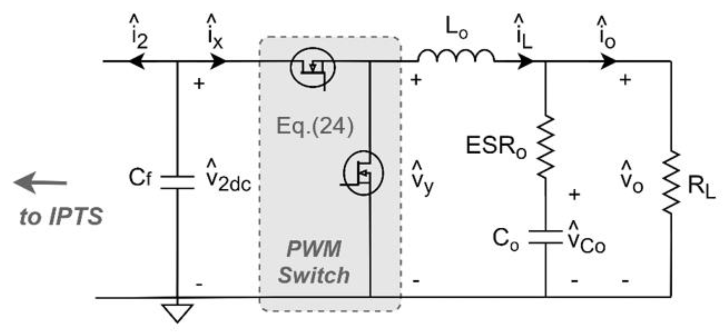
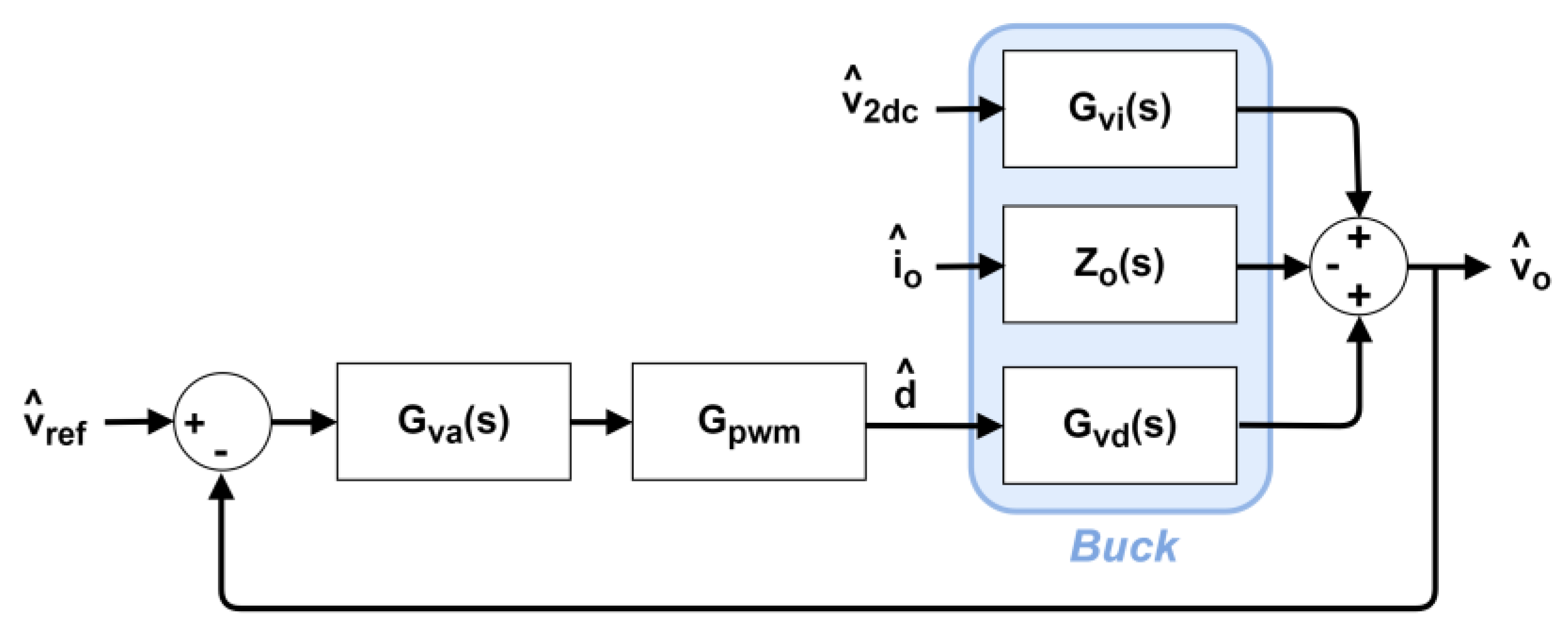
3.2. Small-Signal Modeling of PR-IPTS

Using the IPTS dynamic model presented thus far, it is possible to develop a system-level PR-IPTS model by combining Equations (18)–(23) with the differential equations of the post-regulator. Figure 16 depicts an averaged small-signal equivalent circuit of the buck converter, where the PWM switching cell is replaced with an equivalent two-port AC model described by (24):
i ^ x = D · i ^ L + I L · d ^
v ^ y = D · v ^ 2 d c + V 2 d c · d ^
The “^” operator in (24) denotes the small-signal variations of the considered quantities (note that the duty-cycle variation d ^ is different from the normalized phase-shift d used previously).
The small-signal variation of the buck output voltage can be described by (25):
v ^ o = E S R o ( i ^ L v ^ o R L ) + v ^ C o
which yields (26):
v ^ o = R L E S R o R L + E S R o i ^ L + R L R L + E S R o v ^ C o
Using (23) and (24a), the dynamic equation of the intermediate bus capacitor Cf can be expressed as given in (27):
d v ^ 2 d c d t = 1 C f ( i ^ 2 + i ^ x ) = g 2 C f x ^ D C f i ^ L I L C f d ^
Using (26), the dynamic equation of the buck output capacitor Co can be expressed as given in (28):
d v ^ C o d t = 1 C o ( i ^ L v ^ o R L ) = R L ( R L + E S R o ) C o i ^ L 1 ( R L + E S R o ) C o v ^ C o
Using (24b) and (27), the dynamic equation of the buck inductor Lo can be obtained:
d i ^ L d t = 1 L o ( v ^ y v ^ o ) = D L o v ^ 2 d c + V 2 d c L o d ^ R L E S R o ( R L + E S R o ) L o i ^ L R L ( R L + E S R o ) L o v ^ C o
By combining the IPTS dynamic model (21) with Equations (26)–(29), the seventh-order small-signal model of the PR-IPTS is developed:
d d t x ^ v ^ 2 d c i ^ L v ^ C o X ^ F x f v 2 d c 0 0 g 2 C f 0 D C f 0 0 D L k 1 k 2 0 0 k 3 k 4   A x ^ v ^ 2 d c i ^ L v ^ C o + 0 I L C f V 2 d c L 0 B d ^ v ^ o = [   0 0 k 5 k 6 ] C [ x ^ v ^ 2 d c i ^ L v ^ C o ]
where:
k 1 = R L E S R o ( R L + E S R o ) L o ,         k 2 = R L ( R L + E S R o ) L o ,         k 3 = R L ( R L + E S R o ) C o , k 4 = 1 ( R L + E S R o ) C o ,         k 5 = R L E S R o R L + E S R o ,         k 6 = R L R L + E S R o
Note that in (30), the IPTS input voltage is considered constant with time ( v ^ i n = 0 ). From (30), the state-space solution of the system can be obtained as
X ^ = ( s I A ) 1 B d ^
v ^ o = C ( s I A ) 1 B d ^  
The steady-state operating point of the IPT stage, needed to evaluate (32), can be obtained from the FHA modeling solution (6) presented in the previous section, according to (33):
a 1 = I L 1 L 1 2 ,       a 2 = I L 2 L 2 2 ,           θ 1 = ϕ I L 1 ϕ V 1 ,           θ 2 = ϕ I L 2 ϕ V 1
where IL1, IL2, ϕIL1 and ϕIL2 are the amplitudes and phases of the primary and secondary current phasors I ¯ L 1 and I ¯ L 2 in (6). Let us note that, to evaluate the phase angles θ1 and θ2, all the phase angles obtained from (6) should be decremented by ϕV1 (i.e., the phase of the primary voltage phasor V ¯ 1 ), since in the CMT formulation such ϕV1 term is considered null. Equation (32b) allows to evaluate the duty-to-output transfer function of the buck converter connected to the IPTS:
G v d ( s ) = v ^ o d ^ = C ( s I A ) 1 B
As previously discussed, under certain operating conditions, the buck output voltage can become non-monotonic with respect to the duty-cycle, leading to difficulties in the closed-loop control. Figure 17 depicts the Bode plot of Gvd(s) for the operating point {fs = 70 kHz, V2dc = 14 V} located in the unstable region highlighted in Figure 13d, for the buck parameters listed in Table 2. Indeed, the resulting phase of Gvd(s) is close to −180° at low frequencies, because of the negative static gain Gvd0. This means that the increase in the duty-cycle will lead to the decrease in the output voltage, which is in agreement with the plot of Figure 14a highlighting a non-monotonic Vo vs. D static characteristic. Figure 18 depicts the Bode plot of Gvd(s) for the operating point {fs = 110 kHz, V2dc = 14 V} located in the stable region of Figure 13d. Under such conditions, the static gain Gvd0 is positive, and the Vo vs. D static characteristic is monotonic (see Figure 14c). Hence, this last operating point is feasible for the practical controller design discussed hereafter.

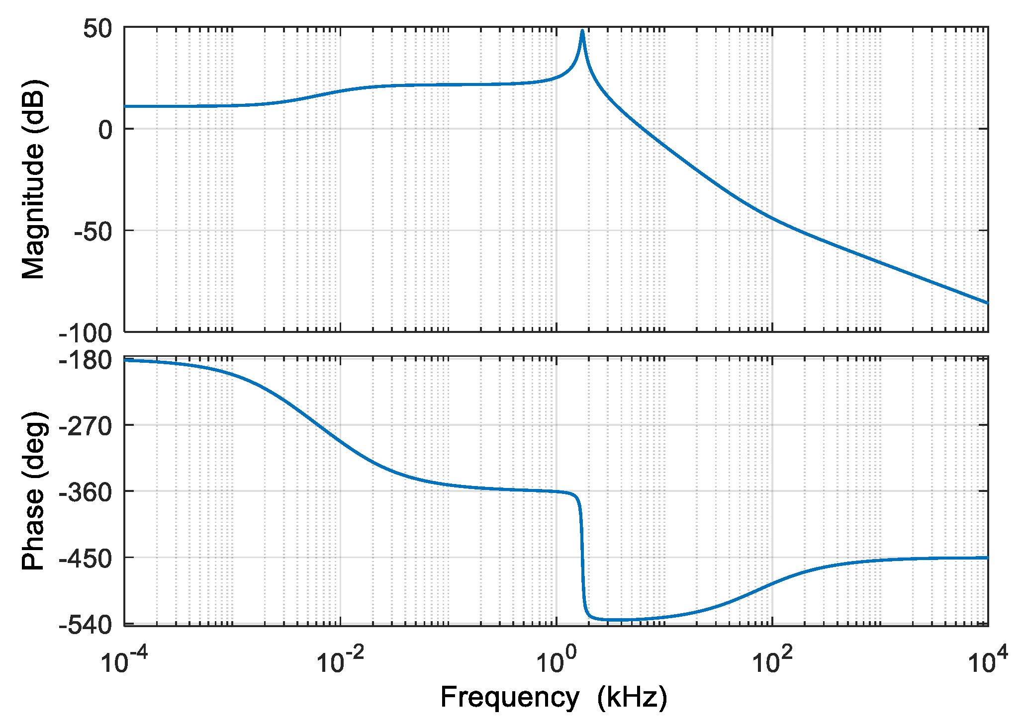
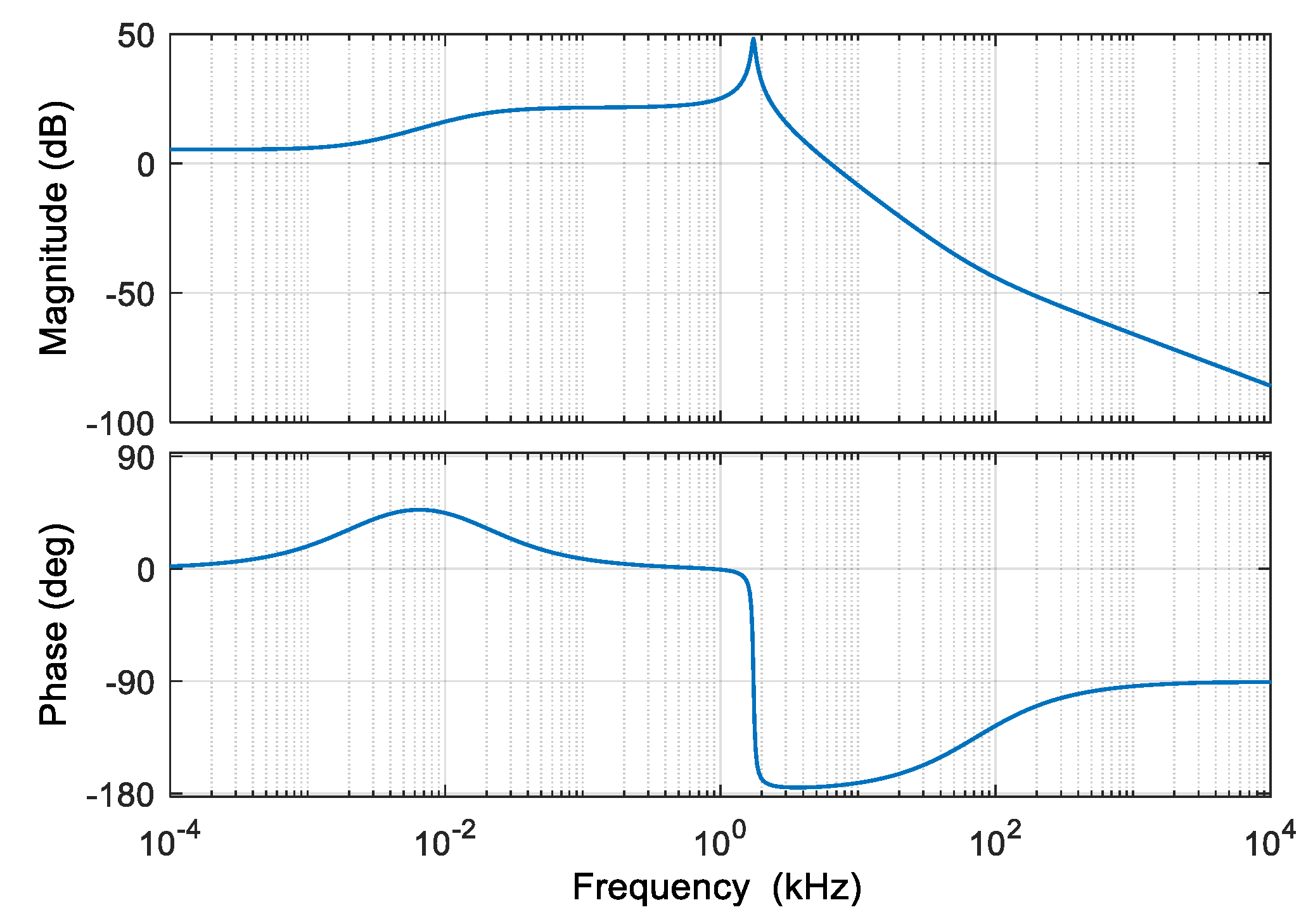
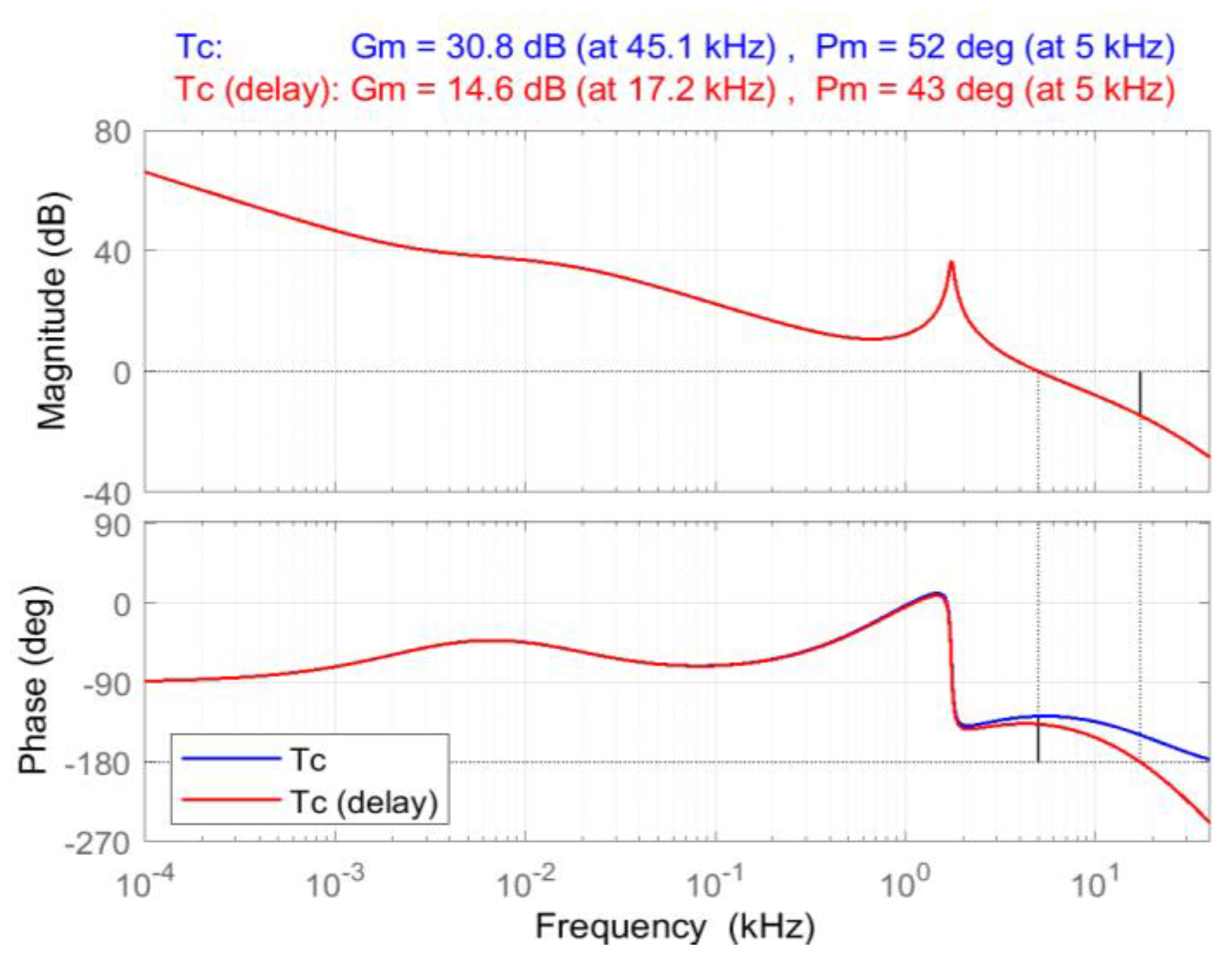
3.3. Digital Voltage Mode Control Design of Post-Regulator

To achieve the buck output voltage regulation, a Digital Voltage Mode Control (DVMC) has been adopted, whose functional schematic is shown in Figure 19. The output voltage vo(t) is scaled down by means of the resistive sensor HV and sampled by the ADC, yielding the feedback voltage vfb[n] in the n-th sampling instant. Such a voltage value is then compared with the digital reference Vref, and the resulting error e[n] is sent to the digital controller which calculates the desired control voltage value vc[n]. The output of the controller is delivered to the Digital Pulse Width Modulator (DPWM) which generates the two complementary driving signals for the buck converter MOSFETs.
To properly design the DVMC, the analog version of the controller has been first developed and subsequently transformed into its digital version. The block diagram representation of the analog VMC is shown in Figure 20, which utilizes a single feedback loop to regulate the output voltage at the desired reference value. The blue box represents the dynamic model of the buck converter including its main transfer functions. The control-to-output transfer function Gvd(s) is provided in (34), while the transfer functions Gvi(s) and Zo(s) can be obtained through the same modeling procedure. The block Gpwm = 1/Vpp represents the PWM gain, where Vpp is the peak-to-peak amplitude of the PWM sawtooth signal (herein, Vpp = 1 V has been used).
The analog controller Gva(s) has been designed by the K-factor method [32], to obtain a given phase margin of the compensated loop transfer function Tc(s) = Gva(sGpwm·Gvd(s) at the desired crossover frequency, ensuring the closed-loop system stability.
Referring to the duty-to-output transfer function of Figure 18, a crossover frequency of fBuck/20 = 5 kHz and a phase margin of 52° have been set, yielding the third-order controller (35) whose coefficients are listed in Table 3:
G v a ( s ) = ω p 1   s     ( 1 + s / ω z 1 ) 2     ( 1 + s / ω p 2 ) 2
To obtain the digital version of such a controller, the Tustin transform (36) has been adopted:
s = 2 f s a m p ( 1 z 1 )   ( 1 + z 1 )  
where the sampling frequency fsamp has been set equal to the buck switching frequency fBuck, so as to synchronize the sampling process with respect to the switching of the converter. Substituting (36) into (35) provides the digital controller transfer function Gva(z) given in (37), whose coefficients are listed in Table 4:
G v a ( z ) = K p b 0 + b 1 z 1 + b 2 z 2 + b 3 z 3     1 a 1 z 1 a 2 z 2 a 3 z 3
where Kp is a scaling factor allowing to adapt the ADC resolution resADC to the DPWM resolution resDPWM [33]:
K p = r e s A D C H V 1 r e s D P W M
The ADC resolution is determined by the ADC full-scale value VFS and by the number of bits used for the quantization Nbit:
r e s A D C = V F S 2 N b i t 1
The DPWM resolution is determined by the number of discrete DPWM levels NDPWM:
r e s D P W M = 1 N D P W M
where NDPWM is determined by a fixed time resolution tres of the DPWM peripheral and by the desired buck switching frequency fBuck according to (41):
N D P W M = 1 f B u c k t r e s 1
where an edge-aligned mode of the DPWM peripheral has been adopted, which allows realizing a desired PWM period by counting from zero up to the NDPWM level and then starting a new period.
Applying the inverse Z-transform to (37) yields the digital control law (42):
v c [ n ] = a 1 v c [ n 1 ] + a 2 v c [ n 2 ] + a 3 v c [ n 3 ] + K p b 0 e [ n ] + K p b 1 e [ n 1 ] + K p b 2 e [ n 2 ] + K p b 3 e [ n 3 ]
Due to the sampling process, the sampled output voltage shows an additive delay, equal to half the sampling period, as compared to the original signal, which may lead to the phase margin erosion of the compensated loop gain Tc(s) that can affect the system stability. Figure 21 shows the impact of the sampling delay on the Bode plots of Tc(s), highlighting that the desired phase margin Pm = 52° of Tc(s) (blue curves) is decreased to Pm = 43° in the delayed version of Tc(s) (red curves). Nevertheless, the closed-loop system stability is still ensured with the acceptable values of both gain and phase margins.
Eventually, the absence of the limit cycle phenomenon has been verified for the proposed DPWM scheme. Limit cycles refer to the steady-state oscillations of vo(t) and other system variables at frequencies lower than the converter switching frequency, which may result from the presence of signal amplitude quantizers such as the ADC and DPWM modules in the feedback loop [34]. Referring to Figure 19, for a given duty-to-output DC gain Gvd0, the duty-to-feedback voltage DC gain is Gvd0 HV. To prevent limit cycles, the change of the feedback voltage ΔVfb(t) determined by the minimum duty-cycle change ΔDmin (corresponding to the DPWM resolution resDPWM) has to be smaller than ADC resolution resADC:
Δ D m i n G v d 0 H V < r e s A D C
The static gain Gvd0 has been estimated by substituting s = 0 in (34). For the presented controller design, the aforementioned parameter values are listed in Table 5. Substituting such values into (43), the absence of the limit cycle has been ascertained. It is worth mentioning that the presence of the IPTS connected to the buck input has caused the static gain reduction as compared to the stand-alone buck regulator for which Gvd0 is equal to the converter input voltage (herein Vin = 14 V). This helped prevent the limit cycle onset which otherwise could occur in the digitally controlled buck converter.

4. Experimental Prototype

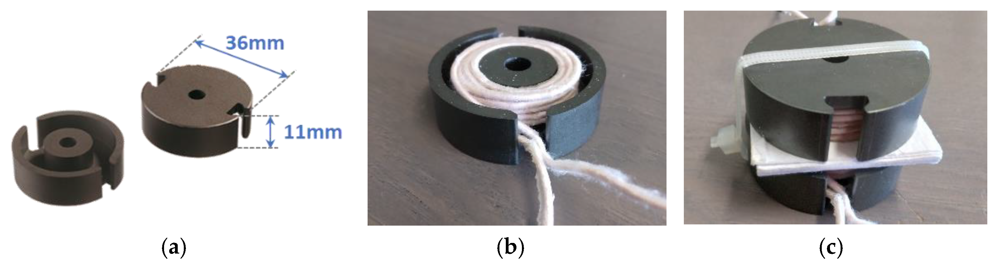
4.1. IPT Coil Realization
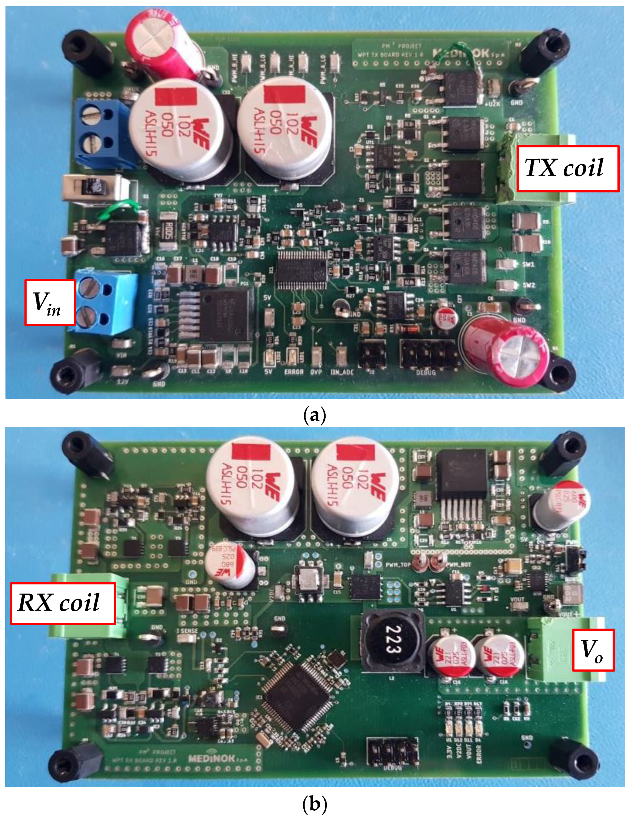
To optimize the overall system performances while maintaining the limited coupling area, custom IPT coils have been herein realized by adopting ferrite pot cores and suitable litz-wires. These latter allow to reduce high-frequency skin and proximity effects in the windings, which could lead to an increase in the resulting AC resistance and power losses [35]. In particular, the Ferroxcube P36/22–3C91 pot cores made of 3C91 ferrite material have been adopted [36] and are depicted in Figure 22a. To realize the windings, litz-wire 170/40 has been used, which is composed of 170 strands of AWG #40 wire, recommended for the operating frequency range [100, 200] kHz. At 200 kHz, the resulting skin depth δ s k i n in the copper wire is higher than the litz-wire diameter dAWG#40, thus allowing to reduce the skin effect:
δ s k i n = ρ C u π µ C u f s = 0.146   mm > d A W G # 40 = 0.08   mm  
where ρ C u = 1.68 × 10⁻⁸ Ω·m and µ C u = 1.256629 × 10⁻⁶ are the copper resistivity and magnetic permeability, respectively. The number of strands (Nstr = 170) allows for the rms current handling capability of the litz-wire given by (45):
I r m s = N s t r ( π d A W G # 40 2 4 ) J r m s = 5.13   A  
where Jrms = 6 A/mm2 represents the maximum allowable rms current density of the copper wire. Thus, the resulting Irms is sufficiently higher than the expected rms current levels in the coils depicted in Figure 13b (see the feasible frequency range from approximately 100 kHz to approximately 150 kHz).
Fifteen turns of the litz-wire 170/40 have been realized on each pot core, and the resulting self-inductances L1, L2 and the DC winding resistances RL1, RL2 have been measured by means of the Extech Instruments LCR200 Passive Component LCR Meter [37]. Such measurement data are listed in Table 6, together with the coupling coefficient values k = M / ( L 1 L 2 ) obtained between the two identical coils for three different air-gap lengths, namely lg = {1.5, 3, 6} mm. The air-gap lg = 3 mm has been herein selected for the final TX and RX coil set depicted in Figure 22c, since such a value yields sufficiently high self-inductances of the coils L1 = L2 = 23 µH and a coupling coefficient k = 0.53, which is a good trade-off solution for the considered application.

4.2. PR-IPTS Boards

An experimental prototype of the proposed PR-IPTS has been assembled using the components listed in Table 7 (refer to Figure 12 and Figure 22 for the IPTS and buck components, respectively). The realized custom Printed Circuit Boards (PCBs) of the IPT TX and RX stages are depicted in Figure 23, with the dimensions of 95 mm × 70 mm × 18 mm and 106 mm × 70 mm × 18 mm, respectively.
On the TX board, the switching frequency and phase-shift modulation of the full-bridge inverter has been digitally implemented through the Infineon 32-bit XMC1302-T038X0064AB microcontroller with ARM® Cortex®-M0 [38], which allows to properly configure the peripherals using the proprietary Integrated Development Environment (IDE) Dave Infineon® [39]. Thus, two PWM signal pairs synchronized at the same switching frequency have been generated from two different DPWM peripherals of the Micro Controller Unit (MCU) and subsequently delivered to the IRS2106SPBF drivers of the two inverter legs [40]. Each PWM signal pair includes two complementary square-wave signals used to drive the high- and low-side MOSFETs of the respective leg, and a 100 ns dead-time has been introduced to prevent a cross-conduction of the switches. To realize a desired phase-shift angle, a delay has been added to the second PWM signal pair with respect to the first one. Both DPWM peripherals have a fixed time resolution tres = 15.625 ns, resulting in a number of discrete digital levels NDPWM which depends on the desired inverter switching frequency fs, according to (46):
N D P W M = 0.5 ( 1 f s t r e s 1 )
where a center-aligned mode of the DPWM peripherals has been set, which allows to realize a desired PWM period by first counting up from zero to the NDPWM level and then down to zero [38]. For the switching frequency fs = 100 kHz, (46) yields NDPWM = 320, while for fs = 200 kHz, it provides NDPWM = 160. The delay between the two DPWM peripherals, needed to implement a normalized phase-shift angle in the range d = [0, 1], can then be realized with discrete DPWM steps in the range [0, NDPWM], resulting in the normalized phase-shift resolution Δdmin given by (47):
Δ d m i n = 1 / N D P W M  
For fs = 100 kHz, (47) yields Δdmin = 0.003125, while for fs = 200 kHz, it provides Δdmin = 0.00625. Hence, the phase-shift resolution is lower than 1% for the switching frequency range of interest fs = [100, 200] kHz.
On the RX board, the DVMC of the buck converter has been realized through the Infineon 32-bit XMC4200-F64X256 microcontroller with the ARM® Cortex®-M4 [41]. Its main peripheral parameters of interest are provided in Table 5, where a high-resolution DPWM peripheral of the XMC4200 MCU has been adopted. The generated complementary DPWM signals are used to drive the buck MOSFETs MHS-MLS through the IRS2011SPBF gate driver [42]. Each of the rectifier MOSFETs M1M4 is switched by the respective IR1161LPBF controller [29], according to the synchronous rectification scheme previously described in Section 2.1.

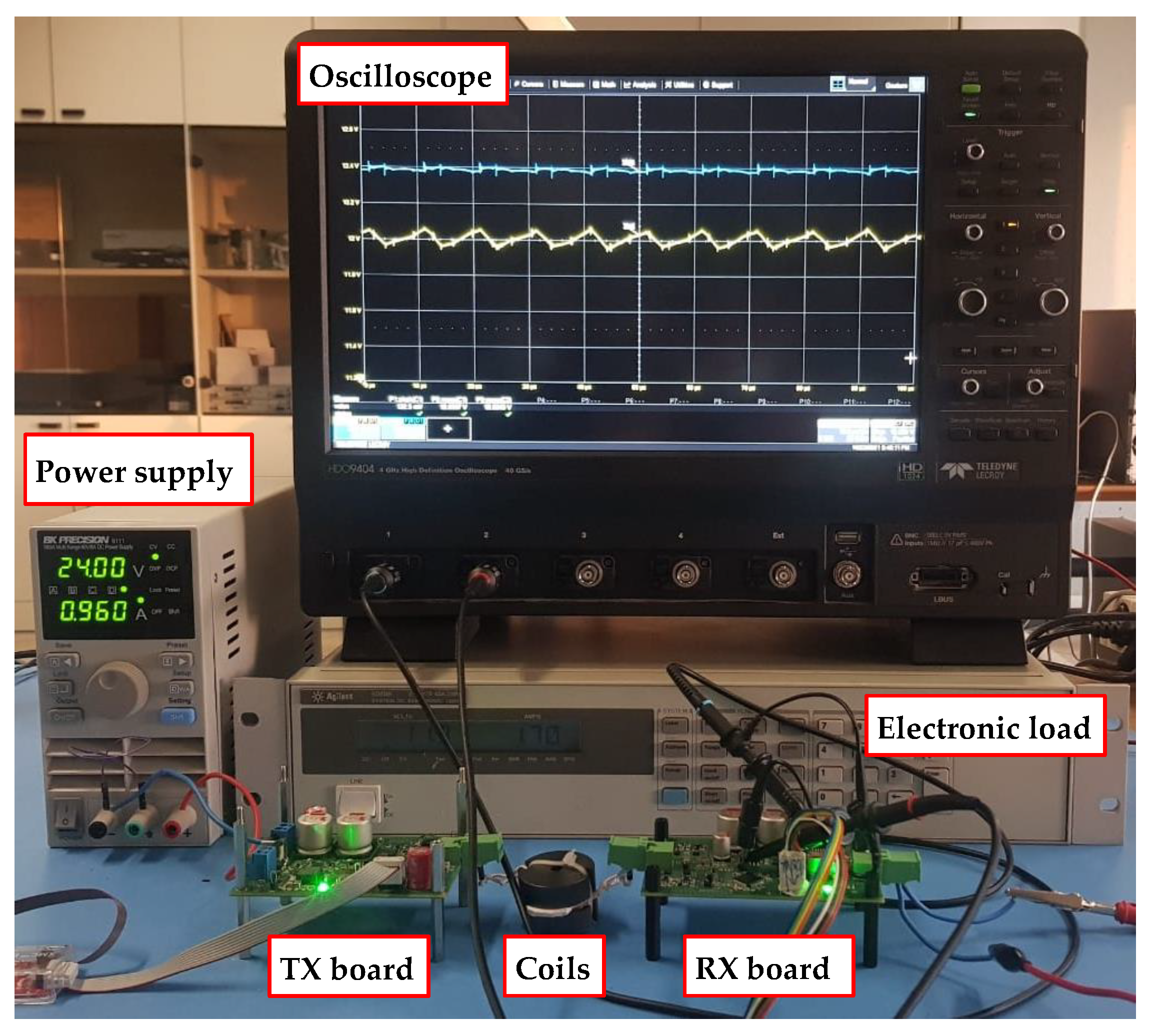
4.3. Experimental Results

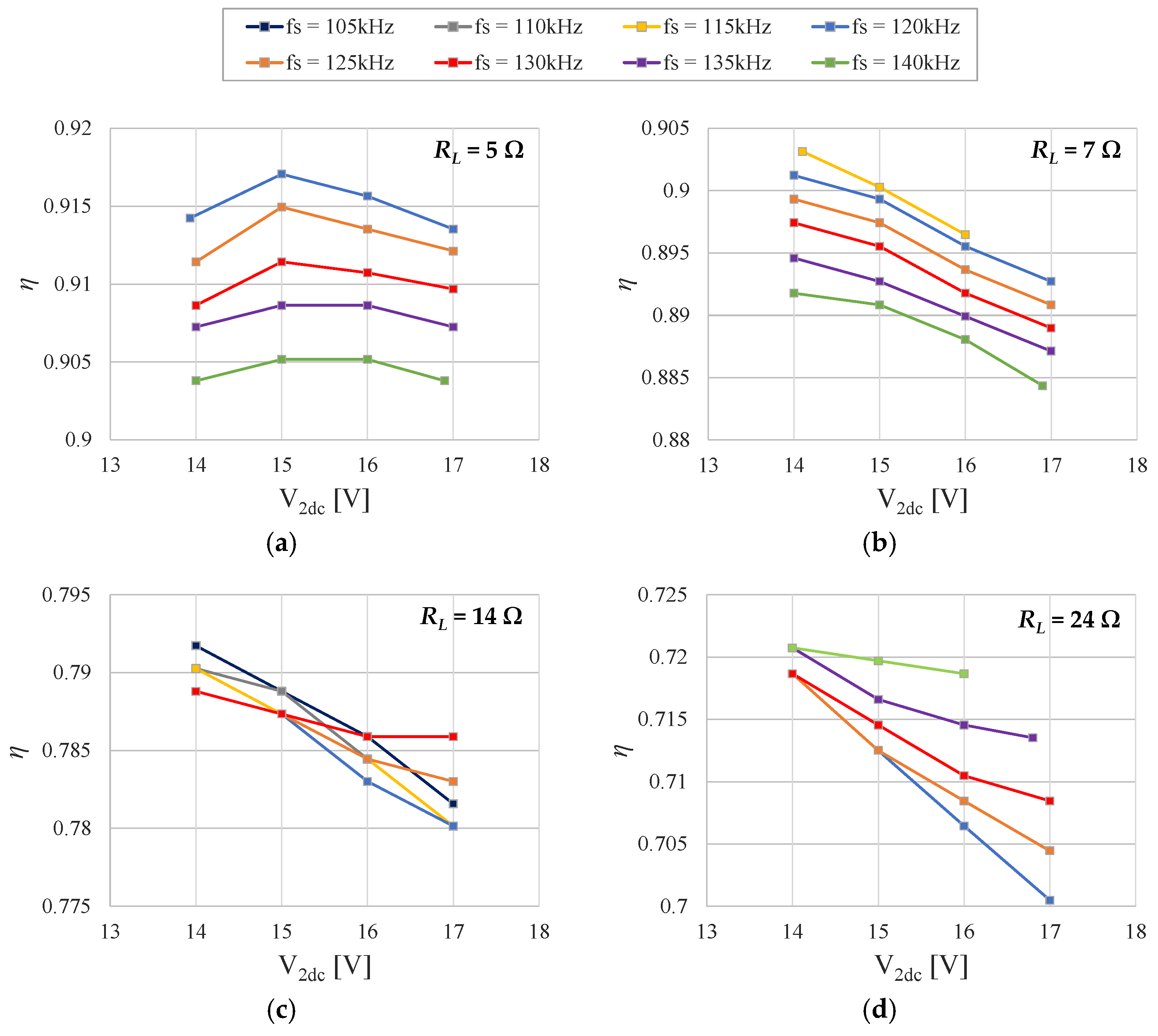
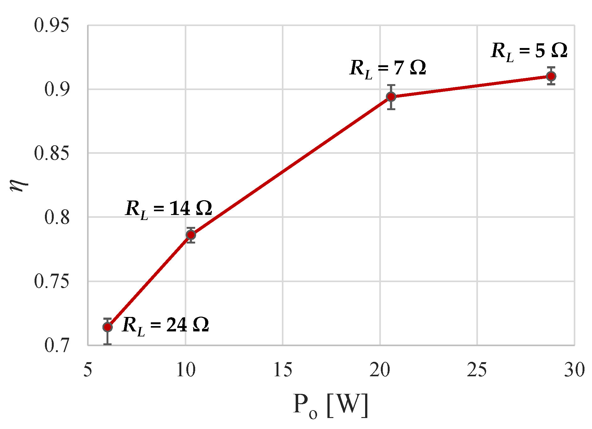
4.3.1. Efficiency Assessment with Electronic Load

The developed PR-IPTS prototype has been tested under different load conditions to assess its power and efficiency performances and output voltage regulating capabilities for variable load demands. Figure 24 shows a complete experimental set-up used during the tests, including the TX and RX boards with the coupling coils, a BK Precision 9111 180 W Multi Range 60 V/8 A DC Power Supply connected to the IPTS input, an HP Agilent Keysight 6060B 300 W 60 A/60 V DC Electronic Load connected to the system output, and a Teledyne LeCroy HDO9404 Digital Oscilloscope.
The overall PR-IPTS efficiency has been measured under four different load conditions RL = {5, 7, 14, 24} Ω (emulated by means of the electronic load configured in the constant resistance mode), which, respectively, correspond to the load power values Po = {28.8, 20.6, 10.3, 6} W. The inverter switching frequency has been varied in the range fs = [105, 140] kHz: for frequencies lower than approximately 100 kHz, the system enters an instable region (blue rectangle in Figure 13d) wherein the buck controller may loose the capability of regulating the output voltage because of the non-monotonic control-to-output characteristic (see Figure 14a,b). On the other hand, for frequencies higher than 140 kHz, the overall high-frequency losses increase yielding the lower experimental efficiency. The intermediate bus voltage V2dc has been varied in the range [14, 17] V while ensuring the output voltage regulation at 12 V: the V2dc values lower than 14 V cannot be realized by the buck converter due to the respective duty-cycle saturation, while the V2dc values higher than 17 V cannot be achieved over the frequency range of interest fs = [105, 140] kHz due to the phase-shift saturation, as previously highlighted in Figure 13a. Figure 25 depicts the resulting experimental efficiencies obtained over the considered ranges of fs and V2dc for four analyzed load conditions. It can be noted that for the heavy loads RL = 5 Ω (Figure 25a) and RL = 7 Ω (Figure 25b), η decreases with fs, for the light load RL = 24 Ω (Figure 25d), η increases with fs, while for the intermediate load RL = 14 Ω (Figure 25c), the efficiency decreases with fs at low V2dc values and increases with fs at high V2dc levels. Figure 25b–d highlight that the efficiency is maximized at V2dc = 14 V for loads RL = {7, 14, 24} Ω, while V2dc = 15 V maximizes η for RL = 5 Ω (Figure 25a). The resulting maximum efficiency points are listed in Table 8 for the analyzed load conditions. Eventually, Figure 26 shows the mean values of the experimental efficiency (red circles, obtained by averaging the measurement data of Figure 25) vs. the output power Po, together with the respective error bars indicating the minimum and the maximum experimental efficiency points. The graph highlights that the average efficiency increases from approximately 71% at Po = 6 W to approximately 91% at Po = 28.8 W.

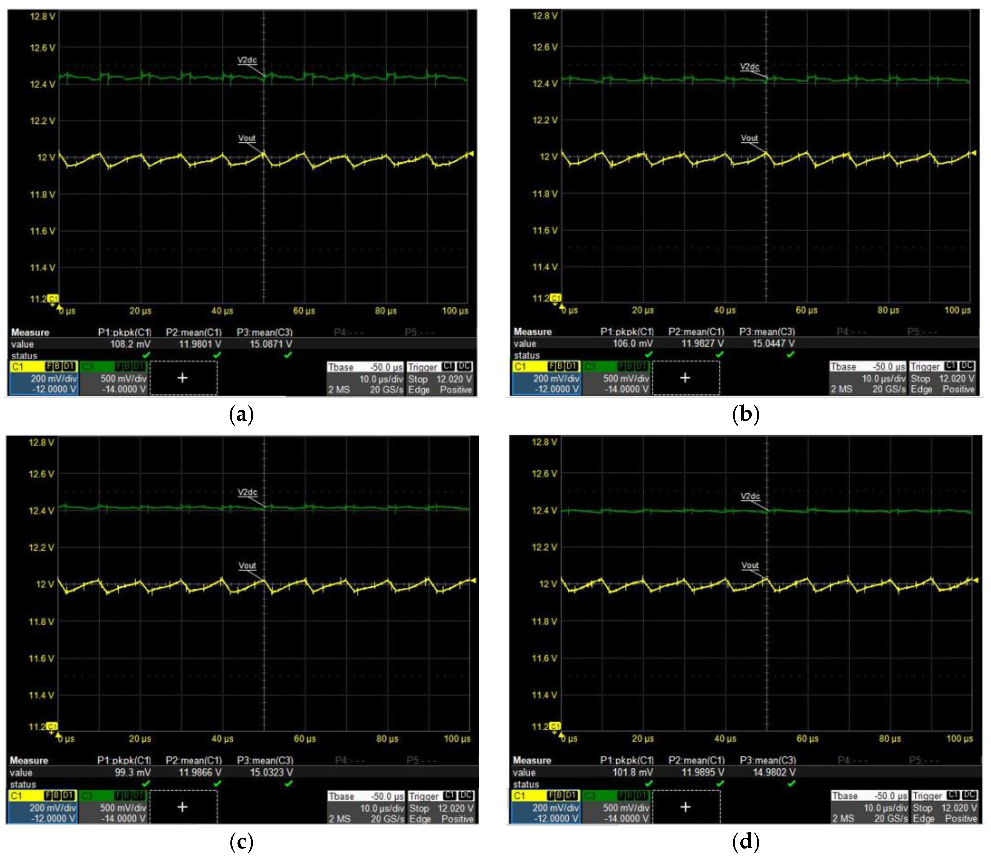
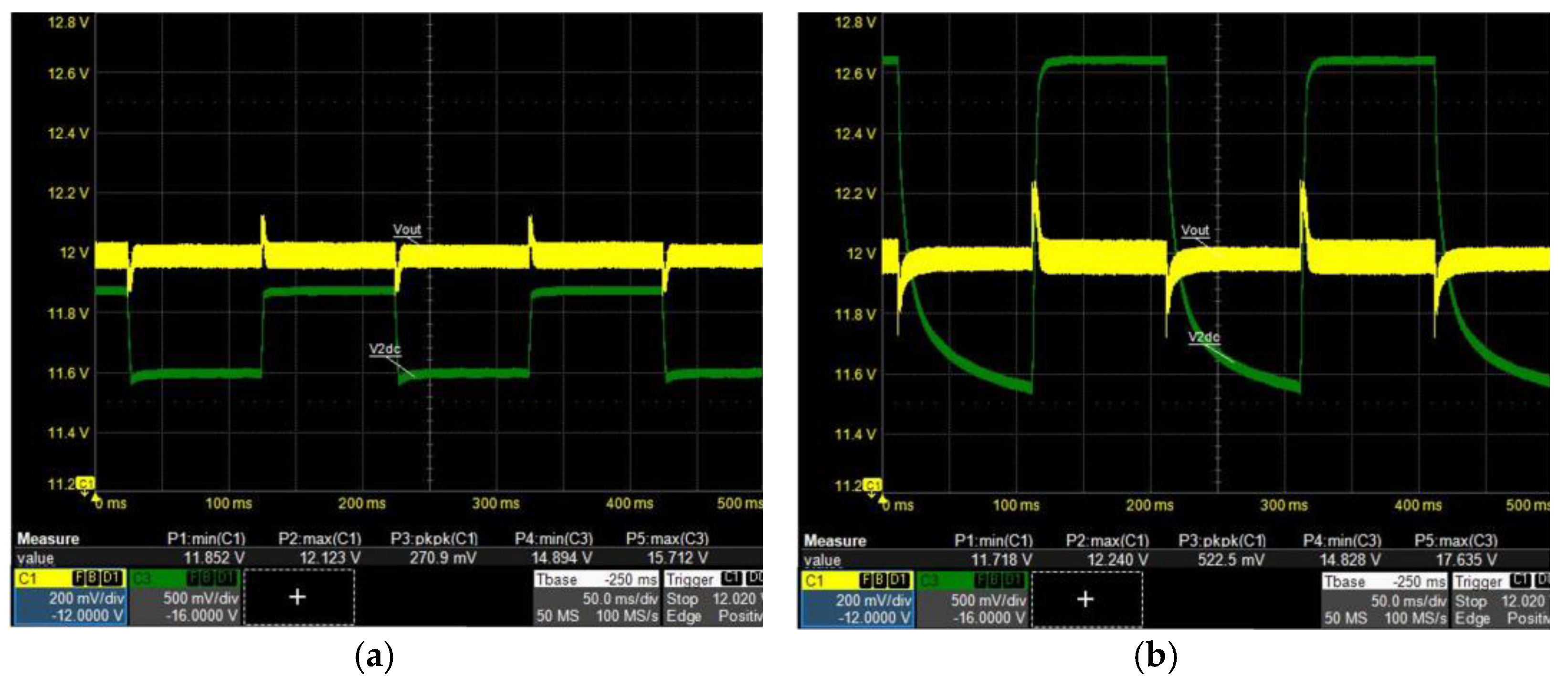
4.3.2. Output Voltage Regulation under Variable Load Conditions

To assess the output voltage regulation capabilities, the IPTS has been tested under both static and dynamic load conditions. Figure 27 shows steady-state experimental waveforms of the output voltage vo(t) and intermediate bus voltage v2dc(t) measured under static load conditions, obtained for the load values RL = {5, 7, 14, 24} Ω at fs = 120 kHz and V2dc = 15 V. The plots highlight that for all the analyzed load levels, the output voltage is correctly regulated at the desired nominal value Vo,nom = 12 V (with an accuracy lower than 20 mV ≈ 0.17% Vo,nom), while the amplitude of the peak-to-peak voltage ripple is limited to 110 mV ≈ 0.92% Vo,nom. Finally, Figure 28 shows experimental waveforms of vo(t) and v2dc(t) measured under dynamic conditions, where the electronic load has been configured to emulate a square-wave variation of the load resistance between 7 Ω and 14 Ω (Figure 28a) and between 5 Ω and 24 Ω (Figure 28b) at a frequency fLT = 5 Hz. Note that such results have been obtained for the inverter switching frequency fs = 120 kHz, while the phase-shift has been adjusted during each test to achieve the intermediate bus voltage V2dc = 15 V at the lower load resistance (i.e., d = 0.621 for RL = 7 Ω in Figure 28a and d = 0.717 for RL = 5 Ω in Figure 28b). From Figure 28a, it can be observed that v2dc(t) presents a step variation between 15 V and 15.7 V as the load resistance changes from 7 Ω to 14 Ω (and vice versa), since the equivalent DC resistance Rdc seen at the buck input also changes, and the IPT stage evolves towards a new bias point. As a result, vo(t) presents over- and undershoots with amplitudes of 123 mV (1.03% Vo,nom) and 148 mV (1.23% Vo,nom), respectively. From Figure 28b it can be observed that v2dc(t) presents a step variation between approximately 14.8 V and 17.6 V as the load resistance changes from 5 Ω to 24 Ω, resulting in the output voltage overshoot and undershoot amplitudes of 240 mV (2% Vo,nom) and 282 mV (2.35% Vo,nom), respectively. It is worth observing that such amplitudes are contained within the typical ranges conventionally adopted for switching regulators (e.g., 5% ΔVo,nom), while the DVMC controller ensures a correct output voltage regulation under load transient conditions.

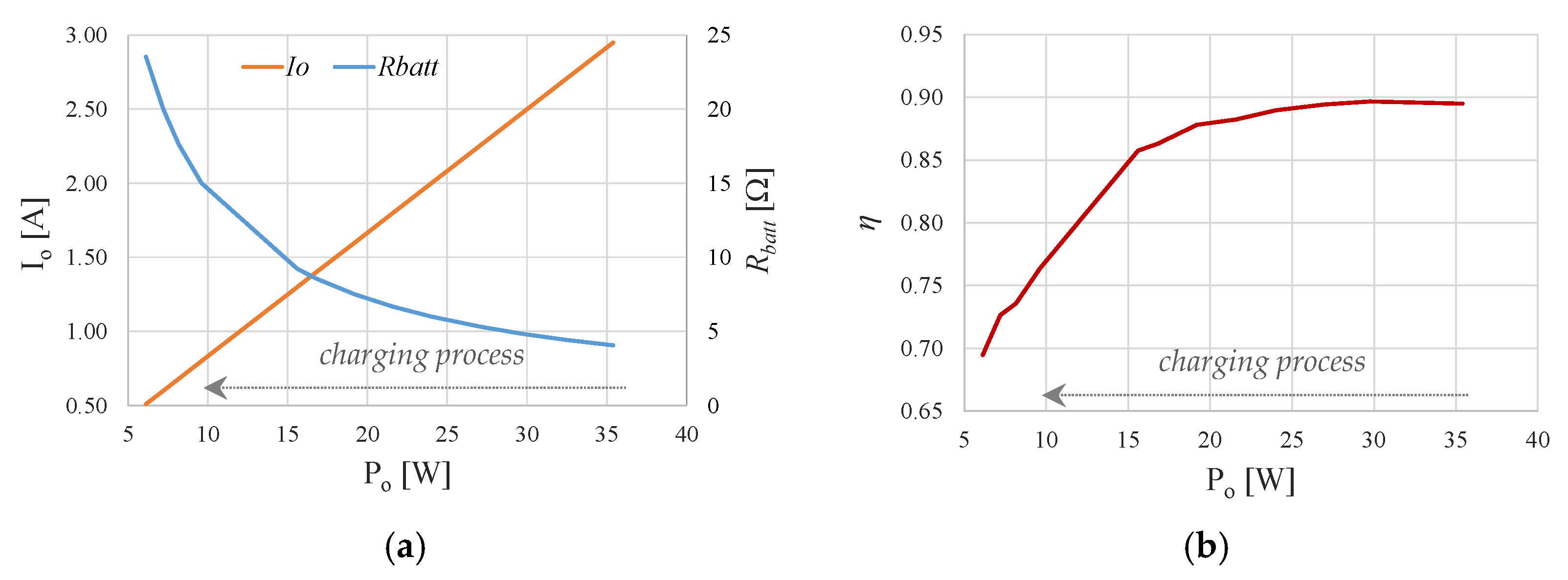
4.3.3. Battery Charging Test

Eventually, the developed PR-IPTS prototype has been used to charge the Aftertech EB-162442275573 Lithium battery with a nominal voltage of 12 V, a capacity of 10 Ah and a maximum recharge current of 3 A [43]. The charging process has been performed in a constant voltage mode by imposing the 12 V regulated output voltage of the PR-IPTS to the battery. Since the equivalent static resistance of the battery, defined as the ratio between the slowly varying voltage and the current, increases during the charging, the tests have been carried out by setting the inverter switching frequency equal to 130 kHz and gradually adjusting the inverter phase-shift to achieve the intermediate bus voltage V2dc = 15 V. During the test, the battery static resistance Rbatt increased from approximately 4 Ω to approximately 24 Ω, as shown in Figure 29a, while the battery current decreased from 3 A to 0.5 A, and the average output power delivered to the battery varied from approximately 35 W to approximately 6 W. The resulting PR-IPTS efficiency is depicted in Figure 29b, confirming that the developed IPT system yields experimental efficiencies higher than 85% over a wide output power range [15, 35] W.

4.4. Results Discussion

The experimental tests presented in the previous section have showed that the developed IPTS is able to correctly perform the output voltage regulation at the desired nominal value of 12 V for static resistive loads in the range RL = [5, 24] Ω, yielding the output power in the range Po = [6, 28.8] W. The experimental efficiencies have been measured over the operating ranges fs = [105, 140] kHz and V2dc = [14, 17] V, highlighting that, for different loads, the efficiency is maximized in different operating points of fs and V2dc as previously reported in Table 8. The achieved maximum efficiencies are of 72.1% for RL = 24 Ω (6 W) and of 91.7% for RL = 5 Ω (28.8 W).
The output voltage regulation capabilities of the presented IPTS have been assessed under different static and dynamic load conditions. For the former, the Vo accuracy lower than 20 mV (0.17% Vo,nom) has been obtained, with a peak-to-peak voltage ripple amplitude limited to 110 mV (0.92% Vo,nom). For the latter, the IPTS behavior has been tested in the presence of load transients, confirming the excellent output voltage regulation capabilities with limited over- and undershoot amplitudes (less than 3% for the worst-case load transient RL = [5–24] Ω).
The system performances have also been assessed during a battery charging test, performed on a commercial lithium battery with a 12 V nominal voltage. It has been shown that the PR-IPTS is able to correctly charge the battery with efficiency levels higher than 85% over the output power range Po = [15, 35] W, while an experimental efficiency of approximately 70% has been obtained for the battery power level of 6 W toward the end of the charging process. These results, obtained for the slowly varying battery static resistance in the range Rbatt = [4, 24] Ω, are consistent with the tests performed for the fixed resistive loads. Thus, the developed system can be effectively adopted to charge both fixed and variable loads.
Eventually, Table 9 and Table 10 provide a comparison between the main IPTS solutions discussed in Section 1.1 and the system developed in this work, highlighting their relevant specifications (Table 9) and functionalities (Table 10).
It can be observed that the system proposed in this work ranks among the best IPTS solutions in terms of efficiency (92%), together with the systems developed in [14,24] having the maximum efficiencies of 90% and 95%, respectively. As regards the IPTS solution presented in [14], it provides a wider output power range (up to 90 W) but a slightly lower maximum efficiency (90%) as compared to our system (92%, 35 W). Both systems are able to guarantee the output voltage regulation, while with respect to the efficiency maximization, the solution of [14] only considers the ZVS achievement yielding a minimization of the inverter switching losses, but does not optimize the overall system efficiency. A complication of the proposed scheme lies in the need for current phase detection circuits on both the TX and RX sides to realize the proposed control strategy.
The solution presented in [24] outperforms our system in terms of efficiency (95%) and is conceived for higher output power levels (3 kW). In comparison, our system presents a limited architectural complexity, since it does not require a pre-regulation and a bidirectional communication link between the TX and RX sides. Even if the latter has a limited implementation cost, the system complexity is significantly increased. Moreover, the solution of [24] does not implement the output voltage regulation which could be a drawback for the loads requiring a stable supply voltage. Such a scheme is mainly focused on the maximum efficiency achievement performed under resonance conditions, but is not valid at different operating frequencies.
Even though our solution does not implement the maximum efficiency tracking scheme, it enables the efficiency mapping with respect to both the inverter switching frequency and the phase-shift. Conversely, previous works [20,21] proposed IPTSs with similar architectural complexities implementing the efficiency maximization by controlling the phase-shift parameter only, but did not consider the inverter frequency optimization. In this regard, our approach provides a more complete and extended characterization of the developed system and addresses the post-regulator controllability issues which instead are not taken into account in the above references. The implementation of control algorithms for maximum efficiency point tracking will be the subject of future works.

5. Conclusions

In this paper, a Post-Regulated Inductive Power Transfer System (PR-IPTS) has been developed, which is based on a series–series capacitive compensation scheme and a DC/DC buck converter used as a post-regulator. Digital control techniques have been implemented by means of low-cost commercial microcontrollers with the objective of ensuring the system efficiency maximization and the output voltage regulation. In this regard, the former objective has been reached through the primary inverter phase-shift modulation performed under different switching frequency and intermediate bus voltage conditions to determine the maximum efficiency points for different loads, while the latter objective has been achieved through the Digital Voltage Mode Control (DVMC) of the duty-cycle of the buck post-regulator. The experimental results performed on a laboratory prototype showed that the developed PR-IPTS yields excellent output voltage regulation capabilities for both fixed and variable loads (including both resistive and battery loads) and is able to deliver up to 35 W output power with a maximum efficiency of 91.7%. The proposed PR-IPTS solution can be profitably used to develop enhanced electronic solutions in the framework of smart homes and workplaces applications.

Author Contributions

Conceptualization, K.S., A.V. and M.C.; methodology, K.S. and A.V.; software, A.V., K.S. and A.A.; validation, K.S., A.V. and M.C.; data curation, A.A. and M.P.; writing—original draft preparation, K.S., A.V., P.V.; writing—review and editing, K.S., A.V. and P.V.; supervision, A.V., M.C., A.A., M.P. and P.V. All authors have read and agreed to the published version of the manuscript.

Funding

This research was carried out as a deep extension of studies into the Project “PM3-Modular Multi-Mission Platform, CUP: B66G18000740005”, Italian Ministry of Education, University and Research call n. 1735/2017, PON Research & Innovation 2014–2020 and FSC.

Institutional Review Board Statement

Not applicable.

Informed Consent Statement

Not applicable.

Data Availability Statement

The data of our study are available upon request.

Conflicts of Interest

The authors declare no conflict of interest. The funders had no role in the design of the study; in the collection, analyses, or interpretation of data; in the writing of the manuscript, or in the decision to publish the results.

References

  1. Ruffo, R.; Cirimele, V.; Diana, M.; Khalilian, M.; La Ganga, A.; Guglielmi, P. Sensorless control of the charging process of a dynamic inductive power transfer system with an interleaved nine-phase boost converter. IEEE Trans. Ind. Electron. 2018, 65, 7630–7639. [Google Scholar] [CrossRef]
  2. Cirimele, V.; Diana, M.; Freschi, F.; Mitolo, M. Inductive power transfer for automotive applications state-of-the-art and future trends. IEEE Trans. Ind. Appl. 2018, 54, 4069–4079. [Google Scholar] [CrossRef]
  3. Yeo, T.-D.; Kwon, D.; Khang, S.-T.; Yu, J.-W. Design of Maximum Efficiency Tracking Control Scheme for Closed-Loop Wireless Power Charging System Employing Series Resonant Tank. IEEE Trans. Power Electron. 2017, 32, 471–478. [Google Scholar] [CrossRef]
  4. Al-Attar, A.; Attia, S.A.; Al-Bialy, A.; Abdelatif, E.N.; Al-Gazar, A.S.; Salem, A.; Badr, B.M. Wireless Power Transfer for Toys and Portable Devices. In Proceedings of the IEEE Conference on Power Electronics and Renewable Energy (CPERE), Aswan, Egypt, 23–25 October 2019; pp. 479–484. [Google Scholar] [CrossRef]
  5. Haerinia, M.; Shadid, R. Wireless Power Transfer Approaches for Medical Implants: A Review. Signals 2020, 1, 12. [Google Scholar] [CrossRef]
  6. Mao, Z.; Han, H.; Zhu, Q.; Su, M.; Peng, T. New concept of wireless power grid for industrial and home application. In Proceedings of the 2018 IEEE International Conference on Industrial Electronics for Sustainable Energy Systems (IESES), Hamilton, New Zealand, 31 January–2 February 2018. [Google Scholar] [CrossRef]
  7. Fadhil, H.A.; Abdulqader, S.G.; Aljunid, S.A. Implementation of wireless power transfer system for Smart Home applications. In Proceedings of the IEEE 8th GCC Conference & Exhibition, Muscat, Oman, 1–4 February 2015. [Google Scholar] [CrossRef]
  8. Mano, M.; Sankar, R. Wireless Charger Networking for Mobile Devices using Bluetooth Technologies. Int. J. Linguist. Comput. Appl. (IJLCA) 2018, 5, 1–3. [Google Scholar]
  9. Wang, C.-S.; Stielau, O.H.; Covic, G.A. Design Considerations for a Contactless Electric Vehicle Battery Charger. IEEE Trans. Ind. Electron. 2005, 52, 1308–1314. [Google Scholar] [CrossRef]
  10. Würth Elektronik, REDEXPERT. Available online: https://redexpert.we-online.com/redexpert/#/ (accessed on 1 September 2021).
  11. TDK, Wireless Power Transfer. Available online: https://product.tdk.com/en/products/wireless-charge/index.html (accessed on 26 August 2021).
  12. Abracon, Wireless Charging. Available online: https://abracon.com/parametric/wirelesscharging (accessed on 27 August 2021).
  13. Zahid, Z.U.; Dalala, Z.M.; Zheng, C.; Chen, R.; Faraci, W.E.; Lai, J.-S.; Lisi, G.; Anderson, D. Modeling and Control of Series–Series Compensated Inductive Power Transfer System. IEEE J. Emerg. Sel. Top. Power Electron. 2013, 3, 111–123. [Google Scholar] [CrossRef]
  14. Liu, F.; Lei, W.; Wang, T.; Nie, C.; Wang, Y. A phase-shift soft-switching control strategy for dual active wireless power transfer system. In Proceedings of the IEEE Energy Conversion Congress and Exposition (ECCE), Cincinnati, OH, USA, 1–5 October 2017. [Google Scholar] [CrossRef]
  15. Ahn, D.; Kim, S.; Moon, J.; Cho, I.-K. Wireless Power Transfer with Automatic Feedback Control of Load Resistance Transformation. IEEE Trans. Power Electron. 2016, 31, 7876–7886. [Google Scholar] [CrossRef]
  16. Li, H.; Li, J.; Wang, K.; Chen, W.; Yang, X. A Maximum Efficiency Point Tracking Control Scheme for Wireless Power Transfer Systems Using Magnetic Resonant Coupling. IEEE Trans. Power Electron. 2015, 30, 3998–4008. [Google Scholar] [CrossRef]
  17. Chen, Q.; Jiang, L.; Hou, J.; Ren, X.; Ruan, X. Research on bidirectional contactless resonant converter for energy charging between EVs. In Proceedings of the 39th Annual Conference of the IEEE Industrial Electronics Society (IECON), Vienna, Austria, 10–13 November 2013. [Google Scholar] [CrossRef]
  18. Berger, A.; Agostinelli, M.; Vesti, S.; Oliver, J.A.; Cobos, J.A.; Huemer, M. A Wireless Charging System Applying Phase-Shift and Amplitude Control to Maximize Efficiency and Extractable Power. IEEE Trans. Power Electron. 2015, 30, 6338–6348. [Google Scholar] [CrossRef]
  19. Fu, M.; Yin, H.; Zhu, X.; Ma, C. Analysis and Tracking of Optimal Load in Wireless Power Transfer Systems. IEEE Trans. Power Electron. 2015, 30, 3952–3963. [Google Scholar] [CrossRef]
  20. Zhong, W.X.; Hui, S.Y.R. Maximum Energy Efficiency Tracking for Wireless Power Transfer Systems. IEEE Trans. Power Electron. 2015, 30, 4025–4034. [Google Scholar] [CrossRef] [Green Version]
  21. Yang, Y.; Zhong, W.; Kiratipongvoot, S.; Tan, S.-C.; Hui, S.Y.R. Dynamic Improvement of Series–Series Compensated Wireless Power Transfer Systems Using Discrete Sliding Mode Control. IEEE Trans. Power Electron. 2018, 33, 6351–6360. [Google Scholar] [CrossRef]
  22. Li, T.; Wang, X.; Zheng, S.; Liu, C. An Efficient Topology for Wireless Power Transfer over a Wide Range of Loading Conditions. Energies 2018, 11, 141. [Google Scholar] [CrossRef] [Green Version]
  23. Di Capua, G.; Femia, N. A Critical Investigation of Coupled Inductors SEPIC Design Issues. IEEE Trans. Ind. Electron. 2014, 61, 2724–2734. [Google Scholar] [CrossRef]
  24. Ishihara, H.; Moritsuka, F.; Kudo, H.; Obayashi, S.; Itakura, T.; Matsushita, A.; Mochikawa, H.; Otaka, S. A voltage ratio-based efficiency control method for 3 kW wireless power transmission. In Proceedings of the 2014 IEEE Applied Power Electronics Conference and Exposition (APEC), Fort Worth, TX, USA, 16–20 March 2014. [Google Scholar] [CrossRef]
  25. Tang, X.; Zeng, J.; Pun, K.P.; Mai, S.; Zhang, C.; Wang, Z. Low-Cost Maximum Efficiency Tracking Method for Wireless Power Transfer Systems. IEEE Trans. Power Electron. 2018, 33, 5317–5329. [Google Scholar] [CrossRef]
  26. Patil, D.; Sirico, M.; Gu, L.; Fahimi, B. Maximum efficiency tracking in wireless power transfer for battery charger: Phase shift and frequency control. In Proceedings of the 2016 IEEE Energy Conversion Congress and Exposition (ECCE), Milwaukee, WI, USA, 18–22 September 2016. [Google Scholar] [CrossRef]
  27. Li, H.; Wang, K.; Huang, L.; Chen, W.; Yang, X. Dynamic Modeling Based on Coupled Modes for Wireless Power Transfer Systems. IEEE Trans. Power Electron. 2015, 30, 6245–6253. [Google Scholar] [CrossRef]
  28. Li, H.; Tang, Y.; Wang, K.; Yang, X. Analysis and control of post regulation of wireless power transfer systems. In Proceedings of the 2016 IEEE 2nd Annual Southern Power Electronics Conference (SPEC), Auckland, New Zealand, 5–8 December 2016; pp. 1–5. [Google Scholar] [CrossRef]
  29. Infineon Technologies, SmartRectifier IR1161LPbF Datasheet. 2016. Available online: https://www.infineon.com/dgdl/ir1161lpbf.pdf?fileId=5546d462533600a4015355c439a5164d (accessed on 28 June 2021).
  30. Hurtuk, P.; Radvan, R.; Frivaldský, M. Full bridge converter with synchronous rectifiers for low output voltage application. In Proceedings of the 2011 International Conference on Applied Electronics, Pilsen, Czech Republic, 7–8 September 2011. [Google Scholar]
  31. Zhang, W.; Wong, S.; Tse, C.K.; Chen, Q. Design for Efficiency Optimization and Voltage Controllability of Series–Series Compensated Inductive Power Transfer Systems. IEEE Trans. Power Electron. 2014, 29, 191–200. [Google Scholar] [CrossRef]
  32. Venable, H.D. The K Factor: A New Mathematical Tool for Stability Analysis. In Proceedings of the 10th International Solid-State Power Electronics Conference (Powercon 10), San Diego, CA, USA, 22–24 March 1983. [Google Scholar]
  33. Biricha Digital Power Ltd., Digital PSU Plant Measurement 2017. Available online: https://www.biricha.com/uploads/8/9/8/0/89803127/digital_plant_measurement_reviewed.pdf (accessed on 21 June 2021).
  34. Peterchev, A.V.; Sanders, S.R. Quantization resolution and limit cycling in digitally controlled PWM converters. IEEE Trans. Power Electron. 2003, 18, 301–308. [Google Scholar] [CrossRef] [Green Version]
  35. Cho, J.; Sun, J.; Kim, H.; Fan, J.; Lu, Y.; Pan, S. Coil design for 100 KHz and 6.78 MHz WPT system: Litz and solid wires and winding methods. In Proceedings of the 2017 IEEE International Symposium on Electromagnetic Compatibility & Signal/Power Integrity (EMCSI), Washington, DC, USA, 7–11 August 2017. [Google Scholar] [CrossRef]
  36. Ferroxcube, P36/22 P Cores and Accessories. 2008. Available online: http://ferroxcube.home.pl/prod/assets/p3622.pdf (accessed on 5 July 2021).
  37. Extech Instruments LCR200 Passive Components LCR Meter. Available online: http://www.extech.com/products/LCR200 (accessed on 6 July 2021).
  38. Infineon Technologies, XMC1300 AB-Step Reference Manual, V1.3 2016-08. Available online: https://www.infineon.com/dgdl/Infineon-xmc1300-AB_rm-UM-v01_03-EN.pdf?fileId=5546d46249cd1014014a0a8436965e28 (accessed on 6 July 2021).
  39. Infineon Technologies, DAVE™—Professional Development Platform for XMC™ Microcontrollers. Available online: https://infineoncommunity.com/dave-download_id645 (accessed on 13 July 2021).
  40. Infineon Technologies, IRS2106/IRS21064(S)PbF Datasheet, No. PD60246. Available online: https://www.infineon.com/dgdl/Infineon-IRS2106-DataSheet-v01_00-EN.pdf?fileId=5546d462533600a4015356763aa527a3 (accessed on 15 July 2021).
  41. Infineon Technologies, XMC4100/XMC4200 Reference Manual, V1.6 2016-07. Available online: https://www.infineon.com/dgdl/Infineon-xmc4100_xmc4200_rm_v1.6_2016-UM-v01_06-EN.pdf?fileId=db3a30433afc7e3e013b3c44ccd35c20 (accessed on 16 July 2021).
  42. Infineon Technologies, IRS2011(S)PBF Datasheet. 2015. Available online: https://www.infineon.com/dgdl/Infineon-IRS2011-DataSheet-v01_00-EN.pdf?fileId=5546d462533600a401535675c19f2784 (accessed on 12 July 2021).
  43. Battery pack 12 V 10 Ah Rechargeable High Quality Lithium F2D5. Available online: https://www.aftertech.eu/pacco-batteria-12-volt-10000mah-10ah-12v-ricaricabile-alta-qualita-litio-f2d5-p-16292.html (accessed on 15 July 2021).
Figure 1. S–S IPTS with passive rectification [13].
Electronics 11 00058 g001
Figure 2. Dual active S–S IPTS with P-PLL&PWM control strategy [17].
Electronics 11 00058 g002
Figure 3. Dual active S–S IPTS with P-CF+S-PWM control strategy [17].
Electronics 11 00058 g003
Figure 4. S–S IPTS with active rectifier and buck post-regulator [18].
Electronics 11 00058 g004
Figure 5. Graphs of voltage VL and current IL delayed by the phase shift φ obtained by varying: (a) the buck duty-cycle D and (b) the active rectifier duty-cycle δ, where Vr is the resulting rectified voltage [18].
Electronics 11 00058 g005
Figure 6. S–S IPTS with passive rectifier and SEPIC post-regulator [22].
Electronics 11 00058 g006
Figure 7. Illustration of the IPTS voltage gain and efficiency including split frequencies [16].
Electronics 11 00058 g007
Figure 8. Closed-loop system structure of the MEPT control scheme proposed in [16].
Electronics 11 00058 g008
Figure 9. Series–series post-regulated IPTS schematic.
Electronics 11 00058 g009
Figure 10. Waveforms example of the phase-shift modulation: MOSFET gate signals (blue) and inverter output voltage (green).
Electronics 11 00058 g010
Figure 11. Predictions of IPTS modeling solution (5)–(8) vs. fs, for different values of C1 and C2: (a) IPTS efficiency η; (b) primary coil rms current IL1rms; (c) normalized phase-shift d for C1 = 100 nF; (d) normalized phase-shift d for C1 = 200 nF.
Electronics 11 00058 g011
Figure 12. Predictions of IPTS modeling solution (5)–(8) vs. fs for different values of V2dc, for the capacitor set-up {C1 = 100 nF, C2 = 100 nF}: (a) IPTS efficiency η; (b) TX and RX coil rms currents IL1rms (solid), IL2rms (dashed); (c) IPTS RX-to-TX voltage gain V2/V1; and (d) normalized phase-shift d.
Electronics 11 00058 g012
Figure 13. Predictions of IPTS modeling solution (5)–(8) vs. fs for different values of V2dc, for the capacitor set-up {C1 = 200 nF, C2 = 100 nF}: (a) IPTS efficiency η; (b) TX and RX coil rms currents IL1rms (solid), IL2rms (dashed); (c) IPTS RX-to-TX voltage gain V2/V1; and (d) normalized phase-shift d.
Electronics 11 00058 g013
Figure 14. PR-IPTS output voltage Vo (top) and intermediate bus voltage V2dc (bottom) vs. buck duty-cycle D for different values of normalized phase-shift d at: (a) fs = 70 kHz; (b) fs = 90 kHz; (c) fs = 110 kHz; and (d) fs = 135 kHz.
Electronics 11 00058 g014
Figure 15. AC equivalent circuit of the IPT stage.
Electronics 11 00058 g015
Figure 16. Averaged small-signal equivalent circuit of the buck converter.
Electronics 11 00058 g016
Figure 17. Bode plots of Gvd(s) for {fs = 70 kHz, V2dc = 14 V}.
Electronics 11 00058 g017
Figure 18. Bode plots of Gvd(s) for {fs = 110 kHz, V2dc = 14 V}.
Electronics 11 00058 g018
Figure 19. DVMC of the buck converter.
Electronics 11 00058 g019
Figure 20. Analog VMC block diagram.
Electronics 11 00058 g020
Figure 21. Bode plots of the compensated loop gain Tc(s) including the sampling delay effect.
Electronics 11 00058 g021
Figure 22. Custom IPT coils realized with Ferroxcube P36/22–3C91 pot cores and litz-wire 170/40: (a) P36/22–3C91 cores; (b) single custom coil; and (c) TX and RX coil set with 3 mm air-gap.
Electronics 11 00058 g022
Figure 23. PCBs of the experimental prototype: (a) TX board; and (b) RX board.
Electronics 11 00058 g023
Figure 24. Experimental set-up used to test the developed PR-IPTS prototype.
Electronics 11 00058 g024
Figure 25. Experimental PR-IPTS efficiency vs. intermediate bus voltage V2dc and inverter switching frequency fs for different load conditions: (a) RL = 5 Ω; (b) RL = 7 Ω; (c) RL = 14 Ω; and (d) RL = 24 Ω.
Electronics 11 00058 g025
Figure 26. Average experimental efficiency vs. output power Po (red circles) with error bars indicating the minimum and the maximum efficiency points.
Electronics 11 00058 g026
Figure 27. Steady-state experimental waveforms of vo(t) (yellow) and v2dc(t) (green) at fs = 120 kHz and V2dc = 15 V for different load conditions: (a) RL = 5 Ω; (b) RL = 7 Ω; (c) RL = 14 Ω; and (d) RL = 24 Ω.
Electronics 11 00058 g027
Figure 28. Experimental waveforms of vo(t) (yellow) and v2dc(t) (green) at fs = 120 kHz and fLT = 5 Hz for different load transient conditions: (a) RL = {7–14} Ω; and (b) RL = {5–24} Ω.
Electronics 11 00058 g028
Figure 29. Experimental measurements obtained during the battery charging test: (a) PR-IPTS output current Io (orange) and battery static resistance Rbatt (blue) and (b) efficiency (red), vs. average output power Po.
Electronics 11 00058 g029
Table 1. IPTS operating parameters and component values.
Vin (V)Vo (V)RL (Ω)L1 (µH)R1 (mΩ)L2 (µH)R2 (mΩ)M (µH)
241272367236412.2
Table 2. Buck converter parameters.
V2dc (V)Vo (V)fBuck (kHz)RL (Ω)Lo (µH)Co (µF)ESRo (mΩ)Cf (µF)
141210072244052068
Table 3. Analog controller coefficients.
ωz1 (rad/s)ωp1 (rad/s)ωp2 (rad/s)
5.99 × 103683.861.65 × 105
Table 4. Digital controller coefficients.
a1a2a3
1.193312123257−0.2026545175060.009342394250
b0b1b2b3
0.824716092259−0.728775227352−0.8219258443040.731565475307
Table 5. Digital control loop parameters used in Equations (38)–(41).
Gvd0HVVFS (V)NbitresADC (V)NDPWMtres (ps)resDPWMKP
1.84740.15223.3128.059 × 10−4204,80048.8284.883 × 10−61084.1
Table 6. Custom IPT coils measurement data.
lg (mm)L1, L2 (µH)RL1, RL2 (mΩ)k
1.535500.75
323500.53
620500.34
Table 7. PR-IPTS components.
Circuit ComponentsValues
Inverter MOSFETs S1S4IPD50N04S4–10: Rds = 9.3 mΩ, Qg = 14 nC
Rectifier MOSFETs M1M4BSZ070N08LS5: Rds = 7 mΩ, Qg = 14 nC
Buck half bridgeBSC0993ND: RdsHS = 4.2 mΩ, QgHS = 13 nC
MOSFETs MHS-MLSRdsLS = 5.6 mΩ, QgLS = 6.7 nC
TX and RX coils L1, L2L1 = L2 = 23 µH, RL1 = RL2 = 50 mΩ
Buck output inductor LoLo = 22 µH, RLo = 23 mΩ
TX and RX compensation capacitors C1, C2C1 = 200 nF, C2 = 100 nF
IPTS input capacitor CinCin = 2440 µF
Intermediate bus capacitor CfCf = 2068 µF
Buck output capacitor CoCo = 440 µF, ESRo = 5 mΩ
Table 8. Maximum efficiency points achieved for the analyzed load conditions.
RL (Ω)Po (W)fs (kHz)V2dc (V)ηmax
528.812015.00.917
720.611514.10.903
1410.310514.00.792
246.014014.00.721
Table 9. IPTS specification comparison.
ReferenceTX/RX Coil SizeAir GapFrequencyPowerEfficiency
This work36/36 mm3 mm100–160 kHz6–35 W72–92%
[13]N/A70 mm165–180 kHz2.5–3.7 kWN/A
[14]N/AN/A95.6 kHz9–90 W74–90%
[16]270/270 mm250 mm515 kHz25–100 W74–79%
[17]100 × 58/100 × 58 mm5 mm50 kHz300–1800W60–77%
[18]43/28 mm3 mm140 kHz1–11 W69–78%
[19]320/320 mm70 mm13.56 MHz40 W70%
[20]27/27 mmN/A97.56 kHz4.5 W65%
[21]310/310 mmN/A100 kHz5.6 W60%
[22]53 × 53/53 × 53 mm12 mm100 kHz1–10 W34–70%
[24]500 × 500/500 × 500 mm100 mm85 kHz3 kW95%
[25]43/43 mm23.5 mm592 kHz0.25–5 W73%
[26]N/AN/A92–110 kHz100–600 W65–78%
Table 10. IPTS functionality comparison.
ReferenceRectification
Type
Pre/Post-RegulationTX–RX
Communication
Output
Voltage
Regulation
Efficiency
Maximization Control
This workSynchronousPostNoYesNo
[13]PassiveNoYesYesNo
[14]ActiveNoNoYesNo
[16]PassivePre and postYesYesYes
[17]ActiveNoNoYesNo
[18]ActivePostYesNoNo
[19]PassivePostYesNoYes
[20]PassivePostNoYesYes
[21]PassivePostNoYesYes
[22]PassivePostNoYesYes
[24]PassivePre and postYesNoYes
[25]RegulatingNoNoYesYes
[26]PassivePostNoYesYes
Publisher’s Note: MDPI stays neutral with regard to jurisdictional claims in published maps and institutional affiliations.

