1. Introduction
It is well known that the Software Defined Radio (SDR) platforms have great versatility to change the system features just by updating the firmware and changing a few components such as the antenna, the filters or the amplifier. La Salle R & D has been working on SDR platform design and performance for the last decade in the framework of a long haul ionospheric radiolink sounder and modem, and the physical layer design [
1]. In this environment, the need for a compact platform to conduct both the sounding and the data transmission for a remote sensing application was considered; this project led us to the design of the IRIS platform, which is presented in this paper.
The project, which used the High Frequency (HF) band, consisted in the transmission of sounding and sensor data from Antarctica to Spain in a 12,760 km ionospheric radiolink, for which we have used several SDR-based platforms designed over the last decade. Part of the study consisted in the sounding of the channel [
2,
3,
4] in order to evaluate channel performance and characteristics. Once the sounding was performed and analysed, the physical layer tests could be conducted [
5,
6,
7], in order to reach the final frame proposal [
8]. This 11-year project gave us the knowledge and the requirements of the optimum SDR platform to be designed to work on a project with such characteristics. In 2015, after closing the physical layer modem design for the long distance radiolink, the group started a new remote sensing HF project, this time using Near Vertical Incidence Sounding (NVIS), a technique which the group had already worked with in the past in terms of ionosphere sounding [
9]. The first prototype of this project has been developed with the IRIS platform [
10], exploiting all its advantages to implement a SDR configurable system.
IRIS is a platform that was designed with the maximum flexibility in order to be used for both educational [
11] and research purposes. Several platforms have been implemented for educational purposes previously such as [
12,
13,
14] . In order to perform all the SDR applications desired, which involve Multiple-Input Multiple-Output (MIMO), the platform requires 2 high speed Analog to Digital Converters (ADCs), 2 high speed Digital to Analog Converters (DACs), and supports different clock input signals and different communication ports enumerated below:
Universal Serial Bus (USB) 2.0 On-The-Go (OTG).
A 10/100/1000 Ethernet connectivity.
A Universal Asynchronous Receiver Transmitter (UART) for low speed communications such as console.
Peripheral Component Interconnect Express (PCIe).
Educational and research purposes have different requirements or restrictions. The educational platforms will be distributed to every pair of students. For this reason, a low cost platform is mandatory while a minimum performance should be obtained. Research purposes usually do not have such a restriction cost, however, the platform permit to adjust the performance of the components to the application requirements.
Table 1 summarises the hardware requirements for both educational and research purposes. It should be noticed that these requirements should be accomplished for educational purposes while for research are desirable.
Finally, IRIS is VITA 57 compliant, in order to add the possibility of expanding it with new Hardware,
i.e., Digital Signal Processor (DSP) units, through a Field Programmable Gate Array (FPGA) Mezzanine Card (FMC) connector. The platform has been designed following Electromagnetic Interference (EMI) rules to obtain the best performance [
15]. These rules have direct implications in the Effective Number of Bits (ENOB) on a design with ADCs or DACs.
The advantage of the versatile design of the platform is that, if it is used for educational purposes, the students are provided with a lite version of the platform, which they can use to develop real software radio applications previously explained conceptually in class. But in the research field, the full version of the platform will be used with the highest design features.
In
Section 2, the state of the art of standard platforms that satisfies our requirements is reviewed,
Section 3 provides the system description of IRIS,
Section 4 shows the measures made over the system performance,
Section 5 and
Section 6 present the applications and the conclusions, respectively.
2. Existing Platforms
Current technology has led to the design of high-performance radio modems that work digitally with bandwidths up to 60 MHz. Therefore, they can directly process Radio Frequency (RF) signals without an external mixer for HF band. The leading FPGAs manufacturers, Xilinx and Altera, mainly propose the use of evaluation boards [
16], as high performance SDR system, with additional subsystems based on the FMC VITA compliant connectors [
17] from third parties such as Terasic, MVD Cores, 4DSP, HiTech Global and Nutaq Innovation, or other manufacturers such as Analog Devices [
18] and Texas Instruments. This solution presents drawbacks in terms of scalability, size and unit cost. The cost can be up to some thousands of dollars which is prohibitive for educational purposes. Moreover the use of multiple boards makes the size bigger than integrated solutions.
Integrated commercial platforms can be divided into two categories: high performance SDR systems such as USRP, 4DSP or Nallatech in [
19,
20,
21] or low cost SDR platform for amateurs and RF enthusiasts such as bladeRF [
22]. These solutions have been developed by non-FPGA manufacturers and partially fit our requirements. They integrate the analog front-end, the processing core and some communication ports. The analog front-end is composed of high speed ADCs and DACs with a throughput ranging from 40 to 125 MSPS and a resolution ranging from 12 to 16 bits.
The higher performance platforms cover our needs of signal integrity and throughput for research applications but their price is too high for an educational platform. Moreover, these platforms have usually a limited number of communication ports such as PCIe, Ethernet or Universal Serial Bus (USB) 2.0 On-The-Go (OTG). The platform presented in this work integrates all communication ports previously mentioned to have more flexibility for some applications such as connecting the platform to a laptop or to an Ethernet network.
The low cost SDR platform covers our requirements for educational applications with low throughput and low resolution converters, for example 40 MSPS and 12 bits. The price of these platforms ranges from $450 up to $1000, while the manufacturer price of the IRIS platform is around $250 for the lite or educational version. Moreover, these platforms are not supplied with a PCIe port for higher throughput applications than the presented in this work.
The platform presented in this work has a good trade-off between performance and cost. To do that, main components or subsystems, such as ADC, DAC, FPGA and clock, are pin-compatible with other families of the same manufacturer to adjust the performance and price to the application. This allows us to decide which ones can be assembled.
3. System Description
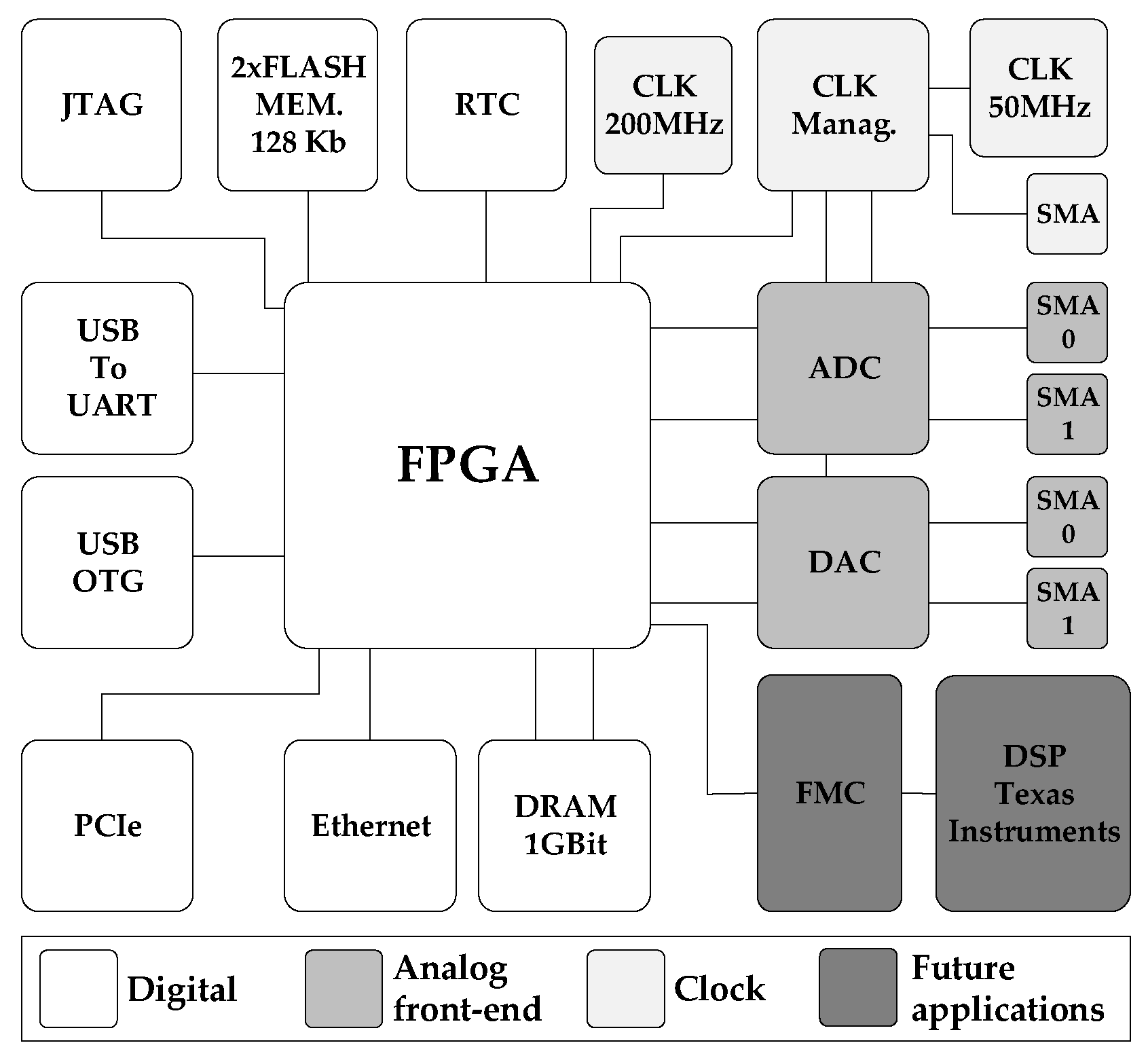
The IRIS platform design takes into account both the requirements of scalability in the performance and the unit cost, minimizing it for educational applications, and easily migrating to a higher performance design when the requirements of the application need it. For this reason, IRIS has been designed with pin-compatible components such as the FPGA, DAC, ADC and the clock input oscillators of the clock manager. To reduce the unit cost, the platform can be built without some additional hardware included in the design, i.e. the Ethernet transceiver, the Synchronous Dynamic Random-Access Memory (SDRAM) memory, the secondary Serial Peripheral Interface (SPI) flash memory which is used for specific applications or the USB OTG. In
Figure 1 the IRIS block diagram is shown.
The IRIS platform has two SPI flash memories, one of them is used to store the FPGA bitstream program file, and the other memory is used to store additional information such as file system or Microblaze [
23] .
Microblaze [
23] is an embedded microprocessor that can be configured as a part of its own hardware in Xilinx FPGAs. This embedded microcontroller allows us to control peripherals with an Intelligent Property (IP) core such as Ethernet or USB OTG through C programming language with a stand-alone application or Linux operating system, which allows easier protocol stack programming than in HDL. Moreover, the system has a volatile SDRAM Double Data Rate type three (DDR3) memory, which is used to store and access data when the application is running at high speed.
The system has 5 communication interfaces: (i) a USB to UART bridge, which can be used to send data at low speed or as a Microblaze console when it is configured on the board; (ii) an Ethernet transceiver able to be configured as 10/100/1000 Mbps; (iii) a USB OTG with a throughput of 480 Mbps; (iv) a PCIe with a throughput of 2.5 Gbps, these interfaces can be used for higher throughput application requirements.
The analog front-end is composed of a dual ADC and a dual DAC, the input and output analog signals, respectively, are injected via SubMiniature version A (SMA) connector. Both signals are single-ended, and they are differentially coupled through operational amplifiers. The high performance analog front-end permits the processing of bandwidths of RF signals ranging from Direct Current (DC) up to 60 MHz.
The clock signal of the converters is distributed via a clock manager, this solution minimizes the jitter and allows to divide the clock frequency of each output. The FPGA unused pins are routed to the FMC connector for future applications.
The IRIS platform has been designed to be versatile, for this reason the platform has a Samtec FMC connector routed following the VITA 57 standard to connect the FPGA to an optional hardware, mainly a Texas Instrument DSP. The interface between the FPGA and DSP through a bus of 64 bits [
24] is planned with 69 pins of 3.3 V CMOS routed to the FMC connector. DSPs are commonly used in radio modems for operations such as Fast Fourier Transform (FFT), coding and applications at baseband.
All components with a SPI port (ADC, DAC, clock distributor/manager, SPI memories and FMC routed) have been multiplexed with 3 chip select signals minimizing the number of pins used. The platform has a Real Time Clock (RTC) connected to the FPGA through an Inter-Integrated Circuit (I2C) port, with the port routed to the FMC connector. These standard ports (I2C and SPI) of the FMC connector will enable future communications between the FPGA and other components.
3.1. Core Processing
The signal processing core is a Xilinx FPGA of the family Spartan-6. The reasons for choosing the integrated circuit are the need of having Gigabit Transceiver Ports (GTPs) for PCIe and the ability to migrate the package from low cost to higher performance.
Table 2 shows us the Spartan-6 family overview. Spartan-6 FPGA with a part number finishing with the letter T have GTPs, for example XC6SLX45T has 4 GTP ports. The 4 GTP ports used are: (i) 1 lane PCIe port, which allows connectivity between the PC and the IRIS; (ii) for future applications, 1 is routed to the FMC connector and (iii) the other 2 are routed to SMA connectors.
The chosen package is the Spartan-6 FG(G)484 because the 45T and 150T with 45 k and 150 k logic cells versions allow us to switch between them them without any Printed Circuit Board (PCB) changes. Higher packages with GTPs than FG(G)484 have been discarded because of their high price.
The chosen devices are XC6SLX45T and XC6SLX150T with FG(G)484 package which have 296 I/O pins, 4 GTPs and the package is a Ball Grid Array (BGA) with a size of 23 × 23 mm.
3.2. ADC
The manufacturers with the highest market impact factor are Analog Devices, Intersil, Linear Technology, Maxim and Texas Instruments. The company with the highest market share is Analog Devices with the 48.5%. For this reason and for previous experience in other projects, Analog Devices is the high speed ADC manufacturer chosen for the IRIS platform.
The filter parameters applied to the search were: a resolution higher than 10 bits and a sampling frequency higher than 60 MSPS (see
Table 3). The design is implemented with the family of highest number of pin-compatible ADCs. The rest of families do not allow us to migrate a design from a throughput of 10 bits to 16 bits. The AD9204 [
25] is pin-compatible with AD9268 [
26], AD9251, AD9258 and AD9231 families permitting a migration of resolution ranging from 10 to 16 bits and a sampling frequency ranging from 60 to 125 MSPS. A particular emphasis is made in AD9204 and AD9268 families because they help to fit the tradeoff between price and performance. The assembled AD converter for educational purposes is the AD9204 which has the lowest performance and the lowest cost. For research applications the assembled AD is the AD9268 which has the higher resolution bit and the highest sampling frequency.
The ADC inputs are differential, so an operational amplifier has been used to make the conversion from single-ended to differential, the integrated circuit used is ADA4938-2 which is a dual ultra-low distortion differential ADC driver [
27].
3.2.1. AD9204
The AD9204 is a dual-channel ADC, which is powered with 1.8 V, has a resolution of 10 bits and sampling frequency of 20/40/65/80 MSPS. It is supplied with a high performance sample-and-hold circuit and on-chip reference voltage. The converter can correct errors of each code with internal logic that provide a precision of 10 bits at 80 MSPS which mitigate the error at higher temperatures. The input clock signals are differential. Optionally an internal duty cycle stabilizer (DCS) can be used to compensate high variations of the duty cycle. The digital output data can be formatted as binary, Gray code or two’s complement. It is supplied with a Data Clock Output (DCO) which is used to register the data in reception. The digital output data supports 1.8 and 3.3 V CMOS depending on the power supply of the digital power supply. The AD9204 is supplied in a Leadframe Chip Scale Package (LFCSP) package of 64 pins.
The sample-and-hold circuit provides excellent performance for input frequencies up to 200 MHz and is designed for low cost and low consumption applications. The standard serial port interface supports some features such as the digital output data format, an internal clock divider, power-down, timing of DCO/DATA, offset adjustment and different reference voltage mode.
3.2.2. AD9268
The AD9268 is a dual-channel ADC with 16 bits of resolution. It works at sampling frequencies of 80/105/125 MSPS. It is designed for communication applications, providing high performance, low cost and reduced size. The input dynamic range can be configured via the SPI port. The ADC also has a DCS to compensate the clock input signal variations maintaining the converter features. The output data bus uses 1.8 V CMOS or LVDS technology. The device programmability and control is done via a SPI communication port.
The AD9268 is supplied in a LFCSP package of 64 pins. Optional Dither On-chip can increase the Spurious Free Dynamic Range (SFDR) level. The converter has an excellent SNR in the entire frequency band. The digital output drivers accommodate the signal to 1.8 V CMOS or LVDS, this allows the use of only a single 1.8 V power supply. The standard serial port interface supports some features such as the digital output data format, an internal clock divider, power-down, timing of DCO/DATA, offset adjustment and different reference voltage mode.
3.3. DAC
As stated before, Analog Devices is the company with the highest market share in analog to digital and digital to analog converters. The search and filter parameters provide higher resolution than 12 bits and sampling frequency higher than 100 MSPS, a brief summary is shown in
Table 4.
The families 911X and 971X are cheaper than the other families. However, only the resolution can be modified, and the frequency clock signal is fixed to 125 MSPS. The last 3 families AD9125, AD9122 and AD9148 have a high clock frequency of 1 Gbps with a resolution of 16 bits, but there are not other cheaper pin-compatible converters with lower features.
The chosen DAC families are AD9745, AD9746, AD9747, AD9780, AD9781 and AD9783 [
28,
29]. These are pin-compatible among themselves and offer us the possibility to use converters with 12 bits and a throughput of 250 MSPS up to 16 bits and 500 MSPS. The assembled DA converter for educational purposes is the AD9745 which has the lowest resolution, lowest maximum sampling frequency and lowest unit cost. For research applications the assembled DA is the AD9783 which has the highest resolution in bits and highest maximum sampling frequency. The DAC outputs are differential and the expected output signal for the antenna has to be single-ended. So, an operational amplifier has been used to make the conversion from differential to single-ended, the integrated circuit used is AD8045 which is an ultra-low distortion high speed operational amplifier [
30]. The main features of these converters are explained below.
3.3.1. Family AD974X
The converters AD974X AD9741/AD9743/AD9745/AD9746/AD9747 of the family AD974X, have resolutions of 8/10/12/14/16 bits respectively, and these devices are pin-compatible allowing the migration from a low resolution of 12 bits to higher resolutions, up to 16 bits. This migration is used to fit the ratio between cost and performance. These dual-channel DACs have a sampling frequency of 250 MSPS and include gain and offset compensation. They are fully programable with a SPI port.
3.3.2. Family AD978X
The converters AD9780/AD9781/AD9783 of the family AD978X, have a great dynamic range and the devices are pin-compatible. These devices are dual-channel DACs with a resolution of 14/15/16 bits and a maximum frequency clock of 500 MSPS. These converters have special features such as gain and offset compensation and a proprietary architecture that allows the synthesis of analog frequencies over the Nyquist frequency moving the energy of the fundamental frequency to the image frequency. These components also are fully programable via the SPI port.
3.4. Clocking System
The clocking system has been designed with the AD9511 [
31] clock distributor of Analog Devices. This clock manager is recommended by Analog Devices for the highest performance converters of our design. The AD9511 has the functionality of distributing the clock input signal to multiple outputs with a core which has a PLL on-chip. The maximum achieved SNR is limited by the jitter at high frequencies as can be observed in Equation (1), where
σ is the jitter,
is the input frequency and
is the SNR when the input signal is at the full-scale, for this reason, the design emphasizes to minimize both the jitter and the low phase noise in order to maximize the signal integrity.
There are 3 input clock signals that can be configured via the SPI port. These inputs can work at frequencies of up to 1.6 GHz. The input voltage level has to be between 150 mV peak to peak and 2 V peak to peak. These inputs are differential, but they can be used as single-ended connecting a capacitor between the negative input and ground. The inputs are CLK1, CLK2 and REFIN as a reference of the PLL circuit. The inputs CLK1 or CLK2 that are not used should be in power-down mode to avoid crosstalk between the inputs.
The PLL circuit is composed of a programable reference divider, a low noise Phase Frequency Divider (PFD), a precision charge pump and a programable feedback divider. The PLL can synchronize frequencies of up to 1.6 GHz connecting an external VCXO or VCO to the inputs CLK2/CLK2B with the REFIN input.
The AD9511 has 5 independent clock outputs. Three of them are standard LVPECL and are able to work at frequencies up to 1.2 GHz, the others can be configured as CMOS or LVDS working at frequencies up to 250 MHz and 800 MHZ respectively. Each output has a configurable integer divider up to 32. The relative phase between 2 outputs can be configured with a phase divider.
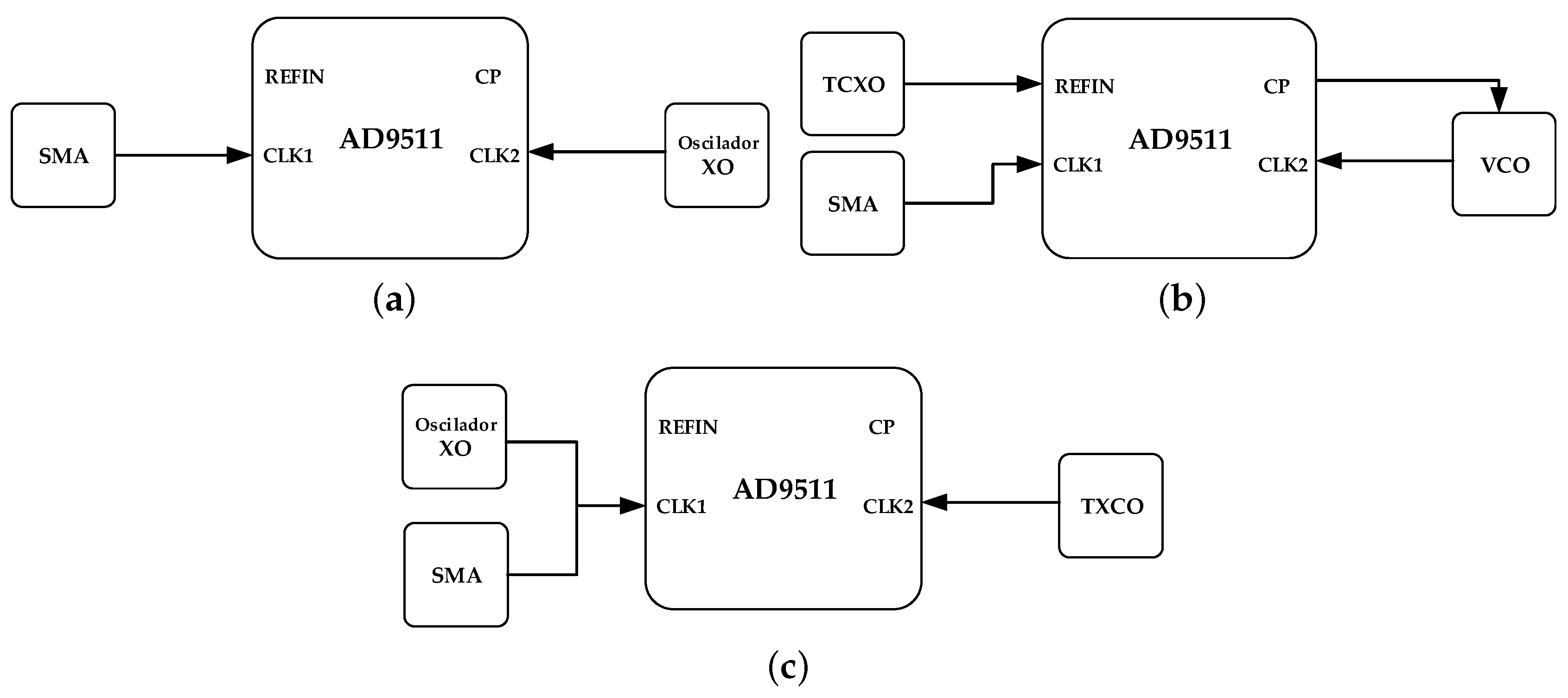
The clock source for the analog front-end converters can be taken either from an external crystal oscillator, a Phase Locked Loop (PLL) frequency synthesizer or an external oscillator as can be seen in
Figure 2. The input clock source has been configured to work with 3 different topologies based on crystal oscillator, VCO using a Temperature Compensated Crystall Oscillator (TCXO) as PLL reference input and TCXO at the work frequency. The components of these inputs are pin-compatible and soldering jumpers on the PCB the clock input configuration can be used. These pin-compatible components can be single-ended or differential soldering some jumpers.
When assembling the desired integrated circuit and the correct jumpers one of the three configurations can be selected. This allows our students to compare and validate how the performance of the clock input signal affects the quality of the analog front-end signals. Moreover, for research applications it enables us to assembly the required clock input signal depending on the desired analog front-end performance.
3.4.1. Crystal Oscillator
This is the lowest performance clock input source because the frequency deviation and jitter are higher than a TCXO which is temperature compensate. However, this solution is the cheapest. The scheme followed is shown in
Figure 2a, where the crystal oscillator is connected to the CLK2 input and a SMA connector to the CLK1 input to allow the injection of an external clock.
3.4.2. VCO Using a TCXO as PLL Reference Input
This configuration uses an accurate clock input source with frequency which is lower than the desired as a reference in REFIN input. The clock input will be generated with a VCO connected to CLK2 input comparing this accurate reference and the VCO signal divided by an integer up to 32. The required signal to adjust the VCO is generated in the PLL and is supplied by the CP pin. This scheme is shown in
Figure 2b, and has better performance than the one based on crystal oscillator because the TCXO has low jitter and low frequency deviation. However, it has a higher cost.
As the crystal oscillator mode the CLK1 input mode is connected to a SMA connector. A SMA connector is wired to REFIN, it will be used to evaluate the output clock performance as a function of different external clock inputs.
3.4.3. Temperature Compensated Crystall Oscillator (TXCO)
The block diagram is shown in
Figure 2c. This is the highest performance and the highest cost solution. The clock input signal is connected to the CLK2 with a TCXO at the desired frequency. This configuration allows injecting signal in CLK1 input with a SMA connector o soldering a crystal oscillator, it can be used to compare the system performance as a function of the input performance clock.
3.5. Communication Ports
This platform can be controlled with 5 different communication ports, 2 UART, a USB OTG, a 10/100/1000 Ethernet and a 1 lane PCI express. This high connectivity allows the student to work from remote places with only a computer and the IRIS. From the scholar point of view, it allows us to use the platform in SDR courses in both the Bachelor and the Master degree, as well as in post-graduate programs. A deeper description about the communication ports is done below:
UART: The system has 2 UARTs, a pair of pins routed directly to a connector and a USB to UART converter. The integrated circuit for the USB to UART converter is the CP2103 from Silabs. This integrated circuit has a configurable output voltage and has been fixed to 2.5 V. For this reason, the converter has been routed to the bank 0 of the FPGA which is powered with 2.5 V.
USB OTG: The USB OTG subsystem can be Host or Device only changing a pair of jumpers. The integrated circuit is the USB3320 [
32] from SMSC, currently Microchip. The USB3320 is a high speed USB 2.0 ULPI transceiver, where ULPI is the physical interface between the integrated circuit and the FPGA, that achieves up to 480 Mbps.
A hardware IP core is required to control the peripheral, translating the microblaze AXI bus to ULPI for host or device application.
The USB peripheral can be used to connect a laptop to our platform for high speed applications up to 480 Mbps or to connect a USB hard drive and save data.
Ethernet: An integrated 10/100/1000 Gigabit Ethernet Transceiver has been used namely 88E1111 model from Marvell [
33]. This integrated circuit supports different MAC interfaces to communicate with the FPGA.
It is well known because it has been used and tested by Xilinx in [
16] and we have designed some applications using it and a Spartan-6 before the integration in the IRIS. It offers a certain flexibility in order to choose a different IP core inside the FPGA to connect it to a microblaze.
PCIe: The PCIe bus is connected to a GTP port, the GTP is a full duplex high speed serial transceiver port able to transmit up to 3.125 Gbps. The PCIe used is one lane width of generation one which can achieve up to 2.5 Gbps.
It is the peripheral with the highest throughput and can be used in applications which require communications between a PC with PCIe and the IRIS.
The jitter in this high speed bus can be a problem. To mitigate it, the jitter attenuator ICS874001L from the manufacturer IDT has been added.
3.6. EMC and Signal Integrity Design Rules
Special attention has been given to Electromagnetic Compatibility (EMC) and signal integrity for a proper design of high speed signals and analog signals.
This section summarizes the best practices studied and applied in the PCB layout. In
Section 3.6.1 the power supply scheme and the filtering are described, in
Section 3.6.2 the impedance matching of microstrip and stripline waveguide is studied, in
Section 3.6.3 the grounding best practice and the improvement it represents is introduced, in
Section 3.6.4 the PCB stack-up is commented and finally in
Section 3.6.5 the track equalization of high speed signal between the DRAM and the FPGA is presented.
3.6.1. Power Supply and Filtering
The power supply has been separated in two groups, analog and digital sources. These power supply outputs have been low pass filtered taking into account the maximum system frequency. Both analog and digital ground planes have been virtually separated and all the components have decoupling capacitors in all power supply pins.
The power supply subsystem of the IRIS is very complex because of the great number of different voltage sources. The FPGA used needs 1.2 V for powering the core up to 3 A, needs 2.5 V, , and need 3.3 V. Moreover, the analog front-end needs 1.8 V, 3.3 V, 5 V and −5 V. These voltage power supply has to be provided by a single source of 9–12 V.
Switched regulators have been used to power the FPGA and the digital parts because of their high current consumption. Moreover, switched regulators are more efficient than linear regulators. The use of linear regulators has been relegated to power analog integrated circuits which demand lower current than FPGA.
The output of a switched regulator has a voltage ripple that can be considered as interference at the harmonics of the switching frequency. These interferences are coupled in the load circuits and can degrade the signal quality when the interference is on the frequency band used. For this reason, a low pass filter with capacitors and ferrites following a pi structure has been used in each output. The accuracy of the analog signals is more sensitive than the digital ones.
The pi filter consists of two input low ESR ceramic capacitors, a ferrite bead with a resonance frequency of 1 GHz and supporting up to 3 A and two output low ESR ceramic capacitor.
Additional capacitances are added to work as decoupling capacitors as close as possible to each power input of each integrated circuit reducing both the inductance presented by the ground plane and the non desirable noise effect produced by one integrated circuit upon another. There are two methodologies for decoupling capacitors connected in parallel, the first is using different capacitors, with capacitance variations of decades, and the second is using the same capacitance values. Previous studies [
15] demonstrate that using capacitors of the same value, the probability of having antiresonance frequency in the decoupling network decreases, for this reason this technique has been applied.
The linear regulator is capable of rejecting the power supply ripple as a function of the load capacitance and the output current, which corresponds to the linear regulator ADP3333 obtained from [
34]. As mentioned before, the analog signals are more sensitive to noise and interference than the digital ones, for this reason, linear regulators are used as analog power supply circuit adding this extra interference rejection, so the lower the frequency, the better rejection. The analog integrated circuits are the ADC, the DAC, the operational amplifiers and the clock distributor.
In order to avoid crosstalk between integrated circuits in the power supply due to the current transient, the more sensitive parts of the analog components have independent power linear regulator such as the power supply pin of the internal clock circuit of the DAC or the 1.8 V analog power supply and 1.8 V digital power supply of the ADC.
A full block diagram of the power supply can be seen in
Figure 3 where ADP5052 [
35], LM2576 and LT3471 are switched regulators, ADP3333 [
34], ADP3335 [
36] and TPS51200 are linear regulators and LPF is the pi low pass band filter.
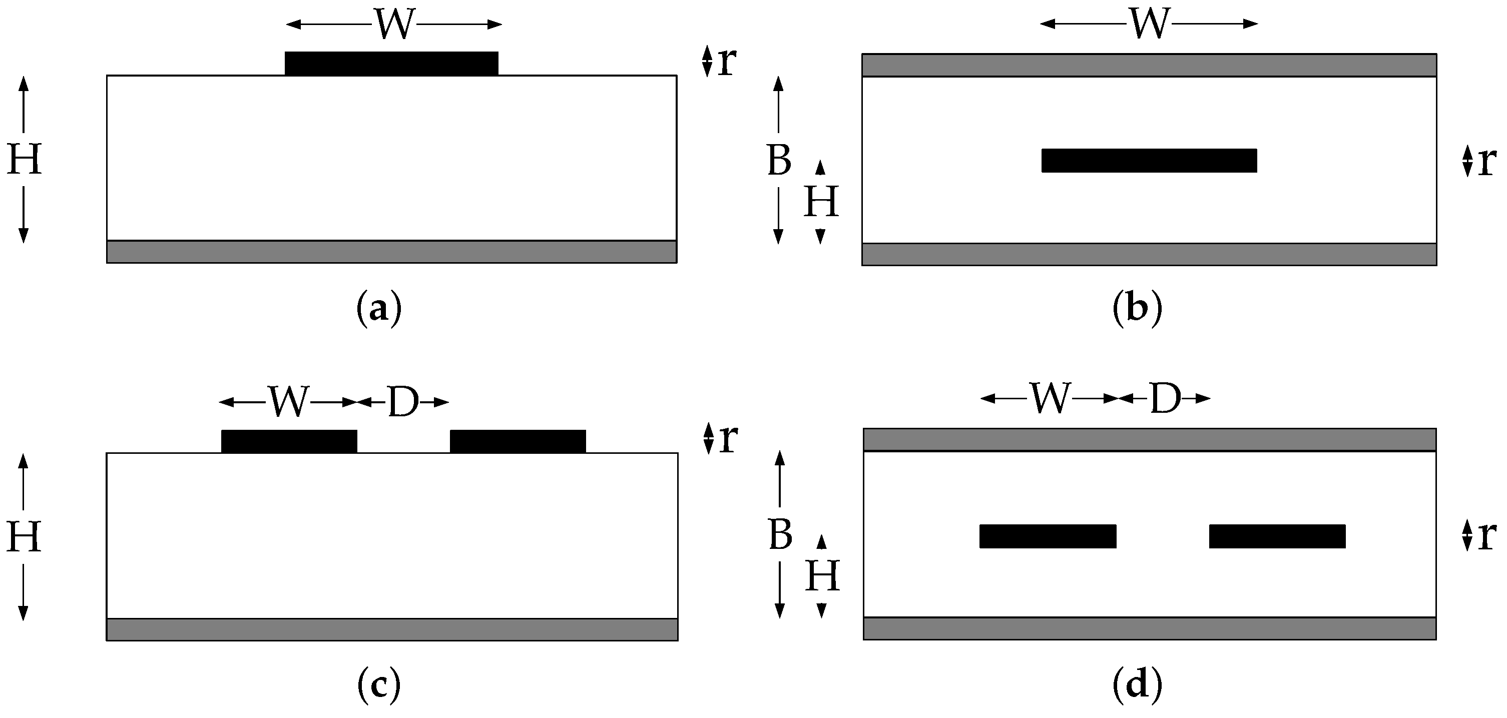
3.6.2. Impedance Matching
When the signal wavelength is comparable to the length of the signal’s track, it can be seen as a waveguide. In
Figure 4 the waveguide microstrip, stripline, differential microstrip and differential stripline used can be seen. The characteristic impedance of the tracks that work as a waveguide has been designed to be 50 Ω for single-ended and 100 Ω for differential pairs, knowing the dielectric characteristics.
This routing consideration to design the tracks has taken into account: the GTP port, the USB OTG, the ADCs, the DACs, Ethernet transceiver, the FMC and the DDR memory.
3.6.3. Grounding
The ground is one of the fundamental ways to minimize noise and it has to be carefully designed. A properly designed ground system can provide protection against interference and emission. The impedance of a conductor depends on the frequency as can be seen in Equation (2).
Any current return through the ground plane presents a difference in voltage Equation (3).
The copper impedance of a track or plane is basically inductive and as digital integrated circuits demand current peaks on each switching, this demands are converted into voltage differences which are coupled to the rest of circuit. The voltage difference that follows the Equation (4) depends on both the inductance and the derivative of the current demanded.
Therefore, an accurate ground design is supposed to minimize the impedance , more precisely, the inductance , and decrease the flow current through a different path. The impedance depends on the geometry of the track or plane, the wider the ground is, the lower the inductance. A full ground plane covering the PCB surface is the solution that presents the lowest impedance, for this reason it was chosen for our design. All the ground connections have been made with via holes between the proximity of the pad and the ground plane.
The stripline waveguide signal appears between two ground or power planes without discontinuities and this is accomplished with full ground and power layer. Moreover, the use of full power and ground in parallel produces an additional embedded low capacitance to the decoupling capacitors. Additional information about the grounding planes can be read in PCB stack-up section.
3.6.4. PCB Stack-up
The selection of the PCB stack-up number of layers has taken into account the following considerations.
Internal signals have to be placed between full ground or power planes to be considered as striplines.
A full power plane in parallel with a ground plane adds.
The higher frequency signals or the more susceptible ones to be disturbed can be routed on internal layers for non-desirable coupling effect reduction.
At least 2 internal layers are needed to route some BGA components such as the FPGA, the DDR memory and the FMC connector.
The PCB thickness has to be 62 mils or 1.6 mm for PCIe standard connectors.
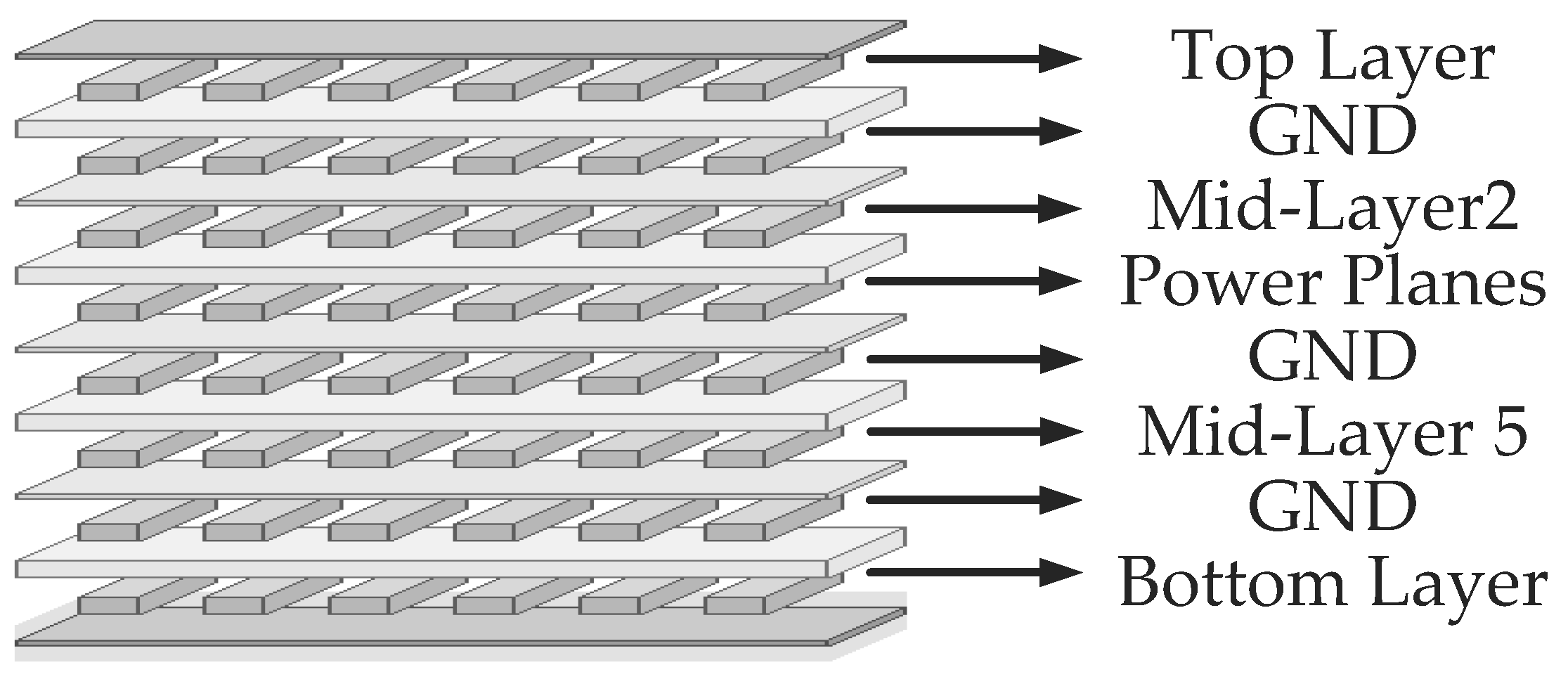
For these reason, a PCB stack-up of 8 layers has been chosen as it can be seen en
Figure 5. The internal Mid-Layer 1, Mid-Layer 4 and Mid-Layer 6 are ground planes, Mid-Layer 3 is the power plane and Mid-Layer 2 and Mid-Layer 5 are the internal layers for routing signals.
Top and bottom layers have been routed as microstrip traces and internal layers as stripline. The internal layers which are enclosed between 2 planes are isolated from external disturbances. The ground plane and the power plane are contiguous layers because the closer the parallel conductive surfaces are, the greater the desirable parasitic capacitance. The selected manufacturing parameters are shown in
Table 5. These parameters have been used to calculate the track widths for the waveguide. This stack-up ensures the required thickness.
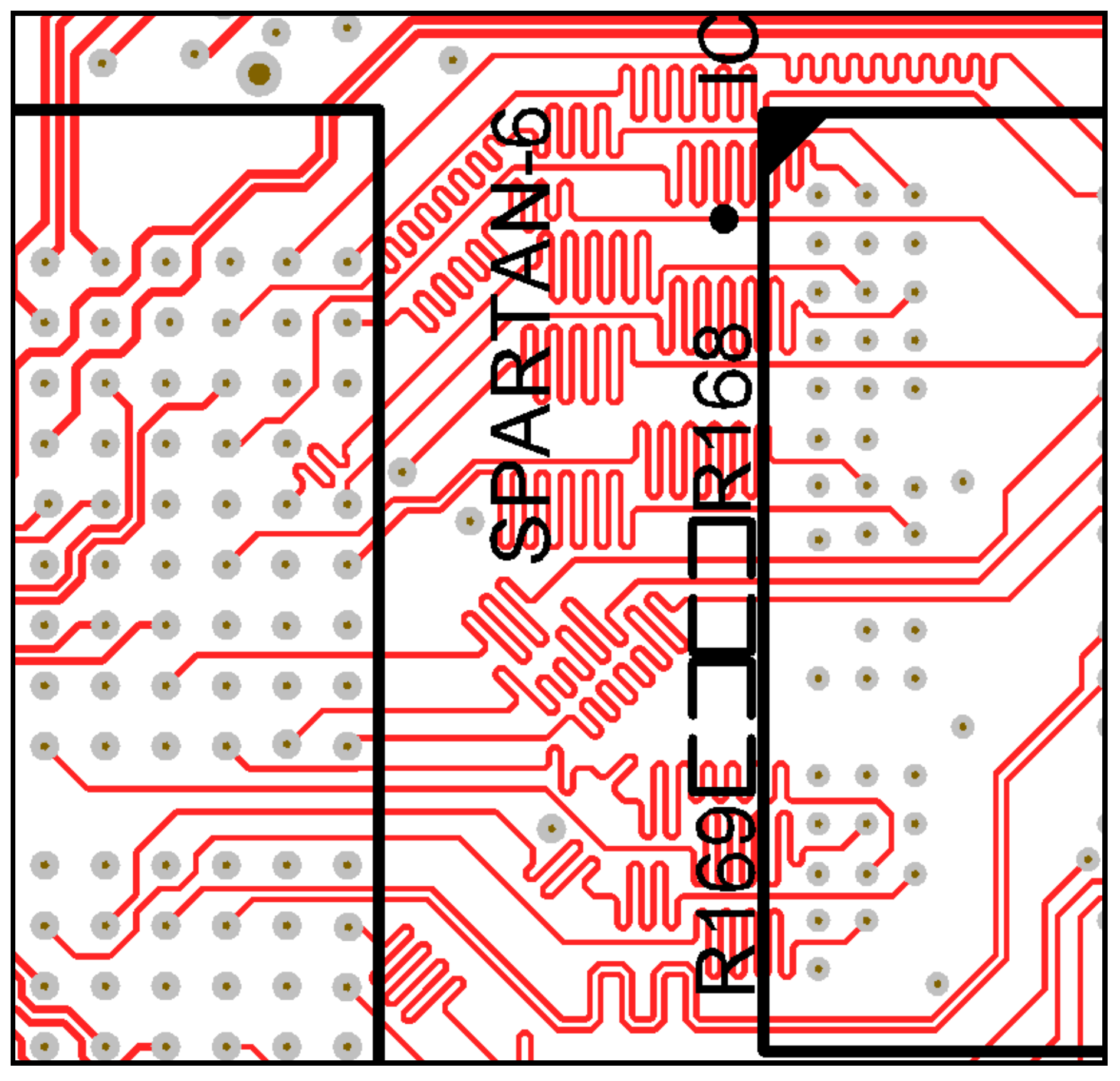
3.6.5. Track Equalization
The design of a high speed digital bus such as the interface between the DDR memory and the FPGA has to ensure that the length tracks are equal. Differences in length between tracks at high frequencies represent a non negligible delay between them. For this reason, as can be seen in
Figure 6, some nets have been extended to obtain the same length. The equalize trace lengths technique places a defined accordion-shaped track extension.
4. Results
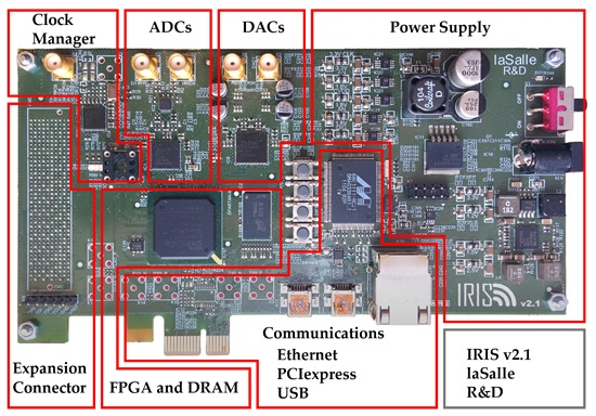
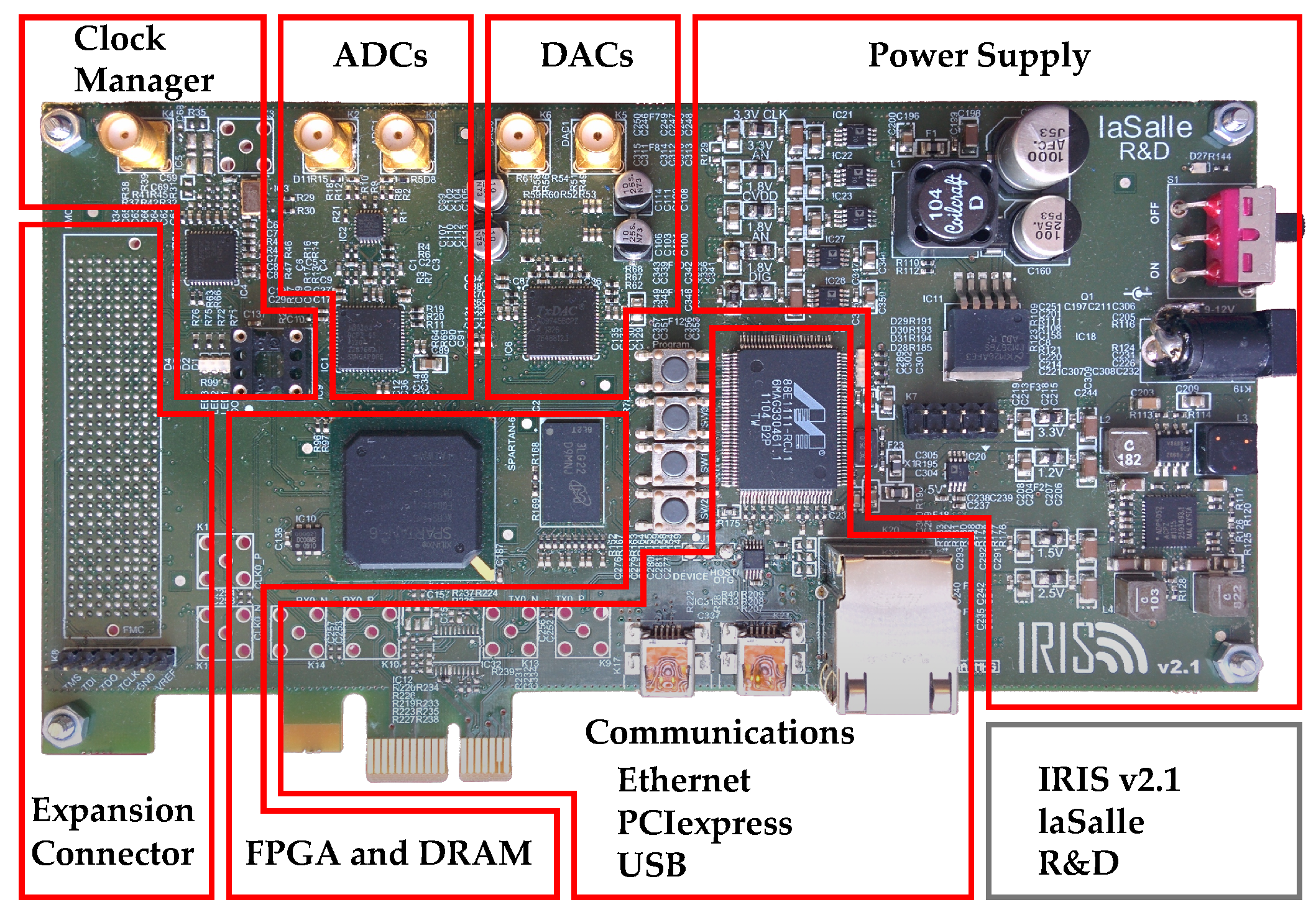
Currently, the IRIS platform for educational purposes has been manufactured and assembled with the lowest performance components. A picture of the platform is shown in
Figure 7.
The ADC is the model AD9204 whith a resolution of 10 bits and a maximum sampling frequency of 65 MHz. The DAC model is the AD9745 with a resolution of 12 bits and a maximum sampling frequency of 125 MHz. Both ADC and DAC have been clocked at 50 MHz with a standard crystal oscillator of the manufacturer FOX.
Measurements of the accuracy in terms of ENOB have been carried out in the analog front-end to check the correct performance of the EMC and signal integrity criterions applied in the design.
The parameters measured for the ADC are described below:
SNR for both the carrier reference (dBc) and the converter full-scale reference (dBFS).
Free Spurious Dynamic Range (FSDR) which is the difference between the full-scale converter and the powerful spurious.
ENOB.
Signal to Noise And Distortion Ratio (SINAD).
Total Harmonic Distortion (THD).
Total Harmonic Distortion plus Noise (THD + N) which is equal to the SINAD when the measures is done from DC to half sampling frequency.
These 6 parameters are defined and considered as basic measures of the ADC dynamic performance in [
37]. However, only the SFDR has been measured because the DDS generated in the FPGA as a source of the DAC has a lower level of SNR than the desirable 73 dB, according to the quantization error formula of the converter which depends on the number of bits.
4.1. ADC Performance Measurement
The ADC sampling measurements require the injection of a pure signal and the analysis of the samples through the Discrete Fourier Transform (DFT) in order to observe the power of the different spurious. The RF signal generator 8642B from HP has been used to inject the input signal to the system. This RF generator has a much better performance than the ADC AD9204 and guarantees a power of non-harmonic distortion below −100 dBc and a phase noise of −138 dBc/Hz at an offset of 20 kHz from the carrier. This performance is better than the approximately 60 dB of SNR that the ADC is able to measure with a resolution of 10 dB. The analysis of the data has been done instantiating an IP core known as chipscope, allowing us to save some signals up to 131,072 samples inside the block RAM of the FPGA and send those signals to the PC via JTAG port. Finally, that data is exported to be read and analysed with Matlab software.
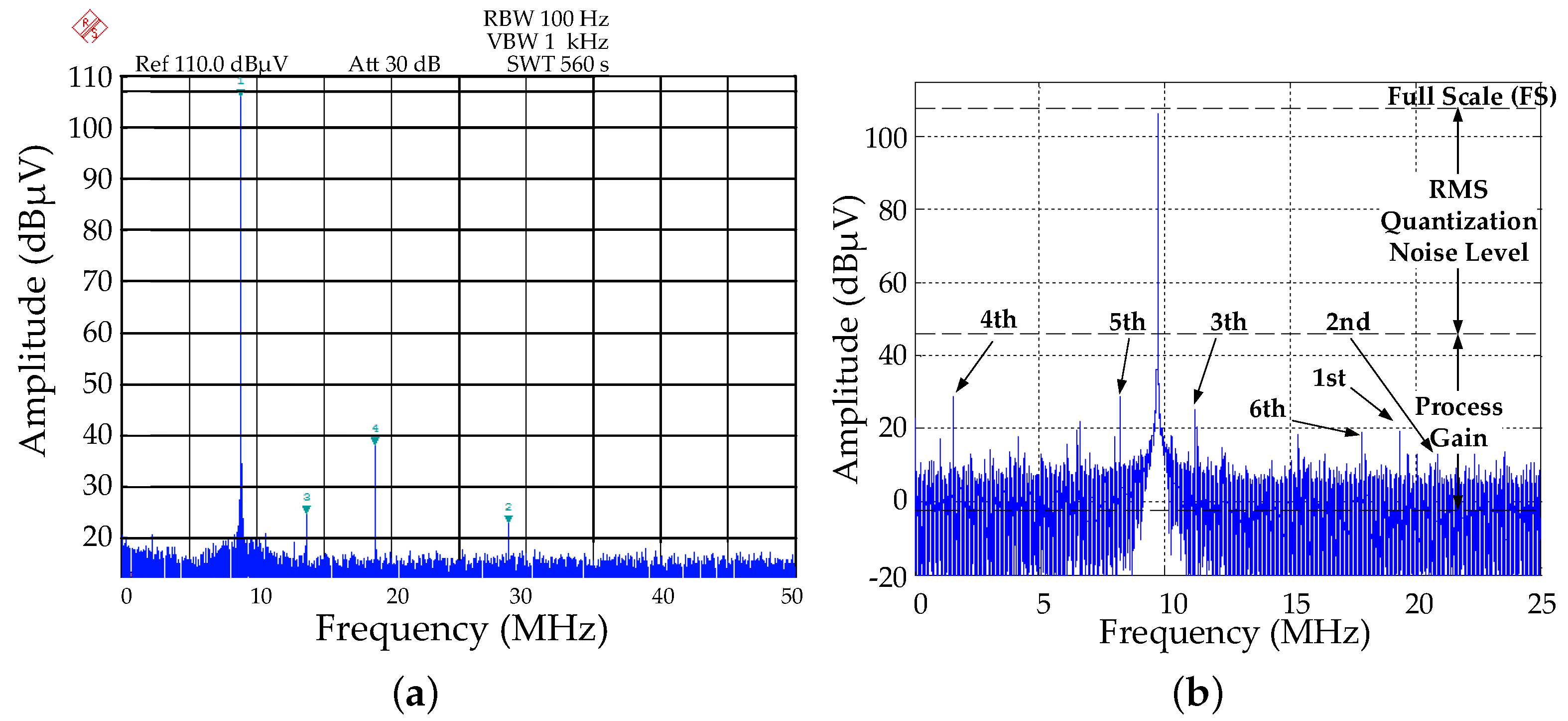
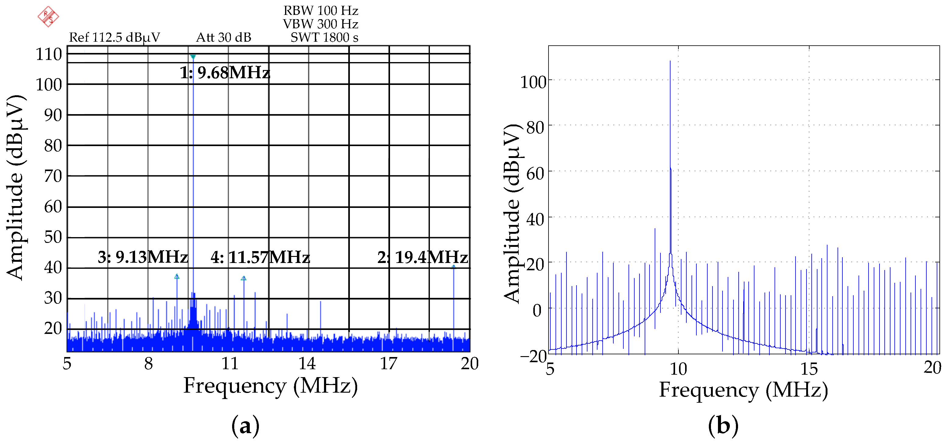
The input signals of the IRIS ADC were analysed with a spectrum analyser to evaluate the accuracy of the signal before the signal is sampled. This input signal spectrum from 1 MHz to 50 MHz is shown in
Figure 8a, where the second and third harmonics are more powerful than the noise floor. However, higher harmonics are less powerful than the noise floor because of the anti-aliasing filter.
All parameters have been calculated from the results obtained in
Figure 8b with Matlab where the full scale, the quantization noise level and the process gain have been drawn. The quantization noise is
dB lower than the full-scale.
The mathematical relationships between ENOB, SINAD, SNR and THD assuming all are measured with the same input signal amplitude and frequency in Equations (
5)–(
8) can be used to help us to obtain all the required parameters. The performance parameters are measured for a bandwidth of 25 MHz which is the Nyquist bandwidth. The noise power
has been calculated integrating the noise over a non-distorted bandwidth and extrapolating it for the 25 MHz of bandwidth and the distortion
D integrating the 8 most powerful spurious.
The values obtained are summarized in
Table 6. The ENOB and the real number of bits of the converter are very similar, 9.78 and 10. It demonstrates that the analog front-end has been designed accurately.
4.2. DAC Performance Measurement
The measurement set-up of the DAC performance has been carried out by injecting the digital samples of a sine wave from the FPGA core to the DAC and evaluating the output of the antialiasing filter with a spectrum analyser. The sine wave has been generated with the DDS Xilinx IP core, the spectrum analysis of the signal generated by the DDS before pass to the converter has been done with Matlab and can be seen in
Figure 9b. The SFDR has been calculated as the ratio between the signal power and the integration of the powerful spourious. The analysis to obtain results has been done from
Figure 9a, the SFDR calculated is 68 dBc and 69.15 dBFs and the quantification noise is
dB, which is 5 dB greater than the SFDR, near to 1 bit in terms of ENOB. Some peaks that appear at the recovering filter at DAC output are generated by the DDS as we can see in
Figure 9b and the noise level generated by the DDS is higher than the quantification noise, for this reason we are not able to measure the accuracy of the converter precisely to obtain more performance values.
6. Conclusions
IRIS is a compact and integrated SDR platform with a high grade of scalability and connectivity, and it follows all the requirements mentioned previously for educational and research purpose applications. The platform has an accurate design in terms of signal integrity and EMC as has been shown in the ADC performance measurements. IRIS outperforms other platforms of the state of the art with the same unit cost, or comparable performances with much less unit cost (see
Table 7),
i.e., the XtremeDSP Development Kit-Virtex-4 Edition with ADCs and DACs resolution of 14 bits has a cost of thousands of dollars. Its analog front-end presents better performance than the IRIS platform with an ENOB of 12.3 bits, which improve our educational version of 10 bits of resolution in 2.5 bits. However, the cost of IRIS is much lower than the XtremeDSP Development Kit. The USRP N200/N210 from Ettus Research, with dual ADCs and DACs of 14 and 16 bits of resolution, respectively, has an ADC SFDR of 88 dBc and DAC SFDR of 80 dBc, which is higher than our 79.2 for ADC and 68 for DAC. Moreover, Ettus platforms come with a powerful software framework and drivers to speed-up the implementation of different applications. However, the cost of this Ettus version is much higher than the IRIS platform, and price is our priority for educational purposes because the aim of this platform is that students and researchers of our University program it at low level focus on the optimization of the algorithms.
Currently, the IRIS is being used as an educational platform for putting into practice some concepts reviewed in the lecturers for both Bachelor and Master of Telecommunications. The feedback obtained from the students is very positive because they have the chance to work with a real platform, and this way they train the transversal competencies and applied work. The great connectivity of the platform allows the students to work from places geographically far from university with only a PC and the IRIS. From the scholar point of view, it allows us to deploy SDR courses and the Master in Telecommunications in an online format using a real system. The system may be connected to an internet network or a Laptop directly using the Ethernet transceiver or the USB OTG.
The IRIS platform can be used for both on-site and on-line programs. The platform was created to apply teaching methodology based on learning by doing [
11] using a real system that the students can use throughout the year in school or at home. Some schools use virtual labs, however, working with a real system helps students reach transversal competencies and increase their knowledge. Finally, for future applications the system can be expanded through the FMC connector, by adding some subsystems such as a DSP to our system.
The IRIS platform has an excellent trade-off between features and cost, to fit the maximum number of applications in both educational and research areas, thanks to the possibility to assembly or not the main different pin-compatible components.


