Transformerless High Step-Up DC-DC Converters with Switched-Capacitor Network


1
Department of Electrical Engineering, Chonnam National University, Gwangju 61186, Korea
2
School of Electrical Engineering and Computer Science, Queensland University of Technology, Brisbane 4000, Australia
*
Authors to whom correspondence should be addressed.
Electronics 2019, 8(12), 1420; https://doi.org/10.3390/electronics8121420
Submission received: 23 October 2019
/
Revised: 20 November 2019
/
Accepted: 26 November 2019
/
Published: 28 November 2019
(This article belongs to the Special Issue Emerging Technologies in Power Systems)
Abstract
:High-voltage gain conversion is necessary for several applications, especially for low voltage renewable source applications. In order to achieve a high-voltage gain, the presented paper proposes a class of transformerless DC-DC converters based on three switched-capacitor networks. The proposed converters have the following characteristics: reduced voltage stress on the capacitors and power devices; obtained high voltage gain with small duty cycle; and reduced conduction losses in the power switches. To verify the operation principle of the proposed converters, the detailed analysis in different conditions of the proposed converters and a comparison considering existing topologies are also discussed in the paper. Moreover, the parameter selection and controller design for the converters are determined. Finally, to reconfirm the theoretical analysis, both the simulation and experimental results taken from a 400 W prototype operating at 60 kHz are given.
1. Introduction
Nowadays, we are facing global surface temperature, the energy crisis and environmental pollution problems. Hence, the use of renewable energy applications is imperatively developed as the most-effective solution. Among various renewable energy sources, photovoltaic (PV) cell, fuel cell (FC) stacks and wind energy have been considered to generate power, as presented in [1]. However, the output of PV, FC cells or wind energy is typically an unregulated, low-level DC voltage and has some drawbacks in [2,3]. Thus, a high step-up voltage gain DC-DC converter is needed to boost to a regulated higher DC voltage bus (200 V or 400 V). Furthermore, the demand for a high boost DC-DC converter has been developed rapidly and popularly. Many high boost DC-DC converters have widely developed and evaluated to find a high-voltage gain in both isolated and non-isolated structures. For the isolated structure, a high-frequency (HF) transformer is added to provide the galvanic isolation between the input and the output with DC/AC and AC/DC power conversions. The isolated DC-DC converters are one of those kinds of converters in which the high voltage gain of the converter can be achieved by adjusting the transformer’s ratio [4,5,6,7,8,9]. Nevertheless, the isolated DC-DC converters have some disadvantages: a high turn ratio is required for high voltage gain applications, which causes more conduction loss of the transformer; the leakage inductance of HF transformer produces voltage spikes across the semiconductor devices; and the snubber circuit is required to reduce the spike and recycle the energy.
For non-isolated structures, the conventional boost DC-DC converter including two semiconductors (one switch and one diode), one inductor and one capacitor is commonly provided to convert a low voltage source into a high DC-bus voltage with simple circuit and low cost. In practice, the voltage gain of the conventional boost converter is limited by the parasitic components. In order to improve the boost ability, the conventional DC-DC converters based on coupled inductor were proposed in [10,11,12,13], however, the leakage problem of the coupled inductor will be caused negative impact for converters. On the other hand, without coupled-inductor structures, the conventional DC-DC converters can be connected in series, but it is very complicated due to the number of switches and control units. For example, the cascade Cockcroft-Walton voltage multiplier was applied to a non-isolated DC-DC converter in [14]. Up to now, many step-up DC-DC converters have proposed to achieve high voltage ratios without isolated transformers or couple inductors. Among these high step-up converters, the quadratic boost converter was proposed in [15] to get high voltage with wide rate of changes using the minimum number of switches. Moreover, some other techniques for high step-up conversions are developed such as interleaved technique [16], voltage multiplier cells [17], switched-inductor cells [18], switched-capacitor cells [19,20,21] or a hybrid of them. The boost ability of transformer-less DC-DC converters in [14,15,16,17,18,19,20,21] is limited because the duty cycle D is varied within a wide range of 0 to 1. When a high boost voltage ability is necessary, the large value of D is reached to 1, this result leads to high conduction loss on the power switches.
In order to provide the boost ability and reduce the duty cycle of the switches in the range of 0 to 0.5, the transformer-less DC-DC converter with Z-source network, which combines two capacitors and two inductors connected in an X-shape, has been presented in [22]. However, the Z-source DC-DC converter operates with discontinuous input current. To improve the input current profile, a converter with switched-boost topology has been introduced in [23], hereby an inductor and capacitor were changed by one more active switch and one more diode. Nevertheless, the output voltage gain of the switched-boost converter is not higher than that of the Z-source converter (G = 1/(1 − 2D)). In [24], a 3-Z network boost converter with three Z-networks has been proposed to get a high step-up voltage. Nevertheless, a large number of passive components in the Z-network leads to an increase in the size, weight, cost and loss of the converter. According to the advantage of switched-capacitor technique, the DC-DC converter with switched-capacitor-based technique have been proposed in [25,26,27,28]. These DC-DC converters can reduce the voltage stress of the capacitors and semiconductors. However, the improvement in the high voltage gain is not very remarkable and may be still not enough for many industrial applications, which come forward a challenge for developing DC-DC converters with even higher voltage gains. In order to further achieve the high voltage gain, a combination of two switched-capacitor cells and energy storage cell has been proposed in [29]. Moreover, a combination of the switched-capacitor cells and switched-inductor cells has been proposed in [30,31]. They still have drawbacks such as a high number of inductors leads to increase the volume, size, cost and reduces the efficiency.
In this paper, a class of high step-up DC-DC converters with three switched-capacitor-networks is proposed and thus named three switched-capacitor-network converters (3-SCNCs). The proposed 3-SCNCs can achieve high gain at low values of the duty cycle and reduce voltage stresses across the capacitors and power devices. Thus, the power switches with low drain-source on-resistance and devices with low nominal voltage can be used in the proposed 3-SCNCs, which in turn reduces the conduction and switching losses. In the next section, the operating principle of the proposed 3-SCNCs in continuous conduction mode (CCM) is given. In Section 3, the proposed converters in both discontinuous conduction mode (DCM) boundary and parasitic components analysis will be accomplished. Section 4 compares the proposed converters with other high voltage gain converters. It is followed by the parameter’s selection of the converters in Section 5. In Section 6, the simulation and experimental results with closed-loop controller will be conducted to evaluate the theoretical analysis. Finally, conclusions are given in Section 7.
2. Derivation of Proposed 3-SCNCs in CCM
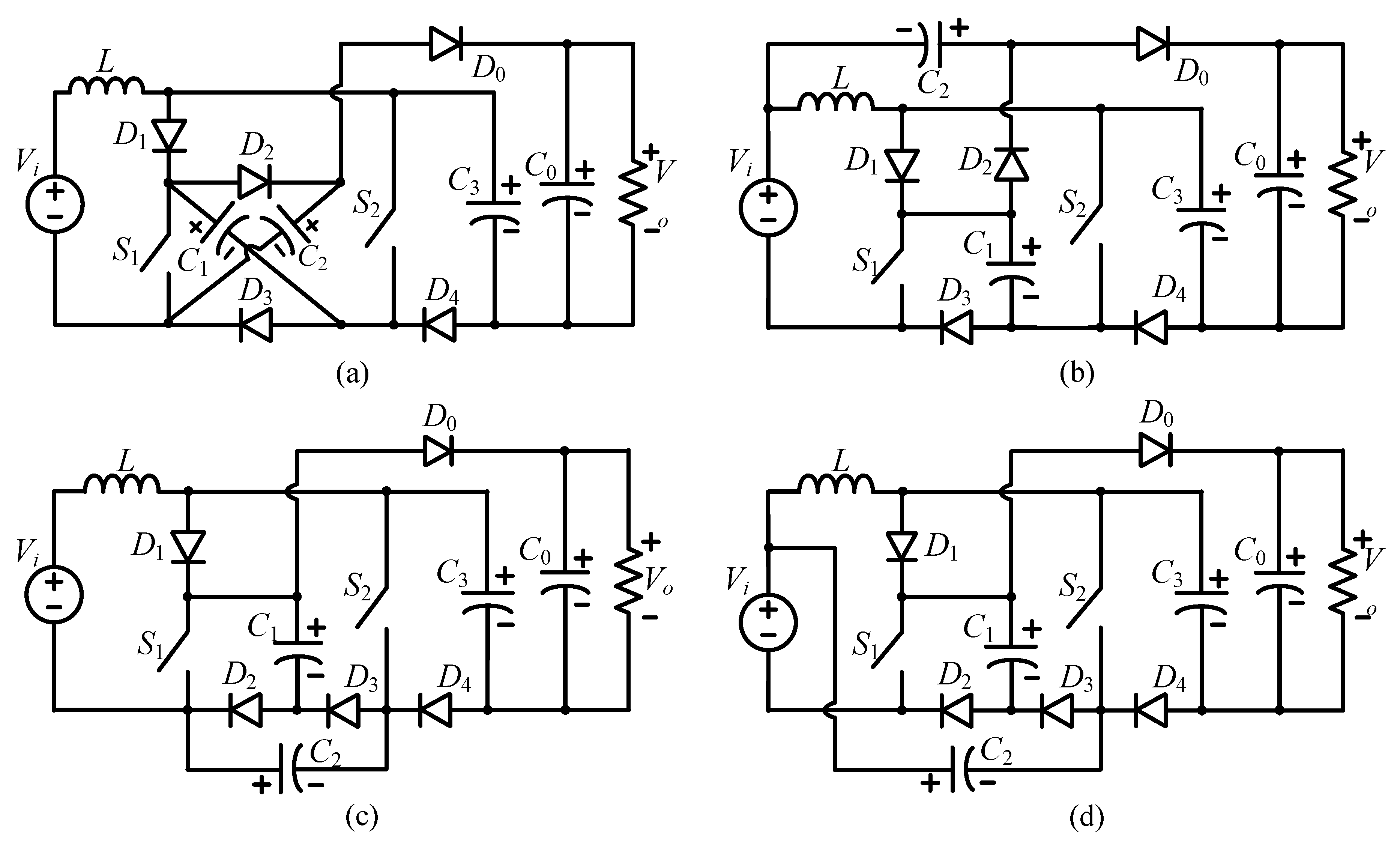
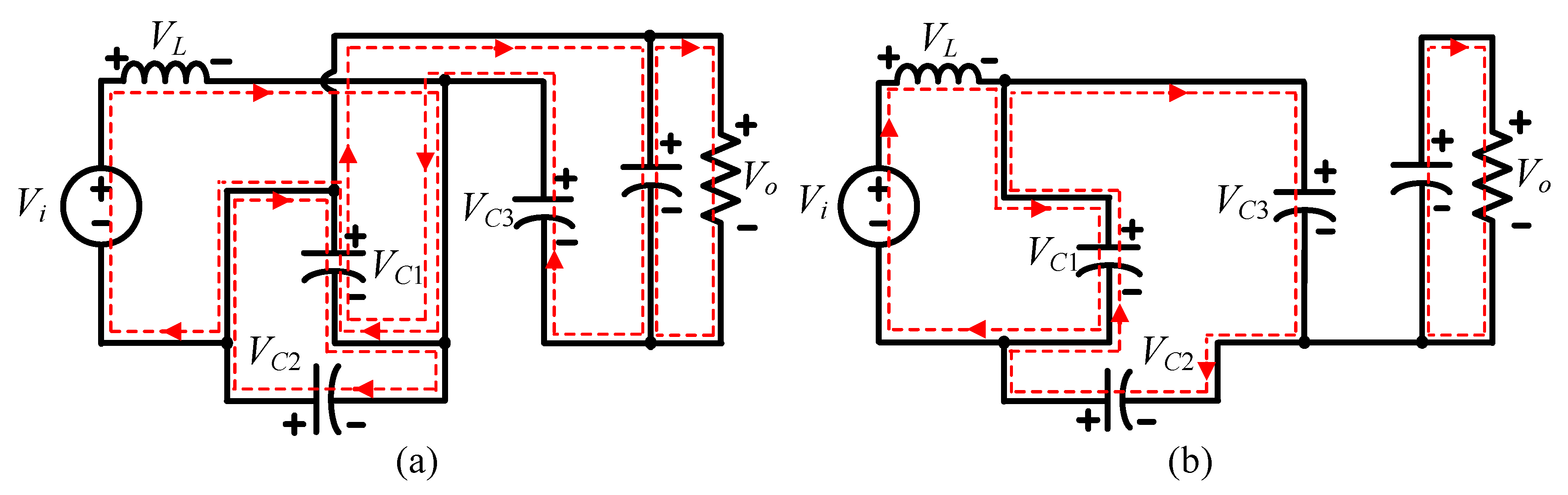
The switched-capacitor-network based converter can provide high voltage gain. By keeping this goal, the basic idea of this paper is to regenerate step-up DC voltage using an inductor and switched-capacitor network during on-state of the switches. The circuit diagram of the proposed 3-SCNCs are depicted in Figure 1. As shown in Figure 1, four proposed converters have the same as several components which contain two power switches (S1, S2), three switched-capacitor networks Dn-Cn (n = 1–3), one boost inductor, one additional diode, and a pair of output diode-capacitor. To simplify the process of theoretical analysis, the following assumptions were made: an inductor current is continuous, all devices are without the effects of parasitic components, the voltage ripple of capacitors are ignored.
2.1. Operating Principle of the Proposed 3-SCNC Type 1
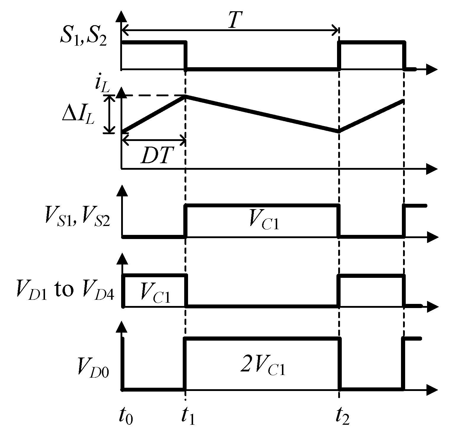
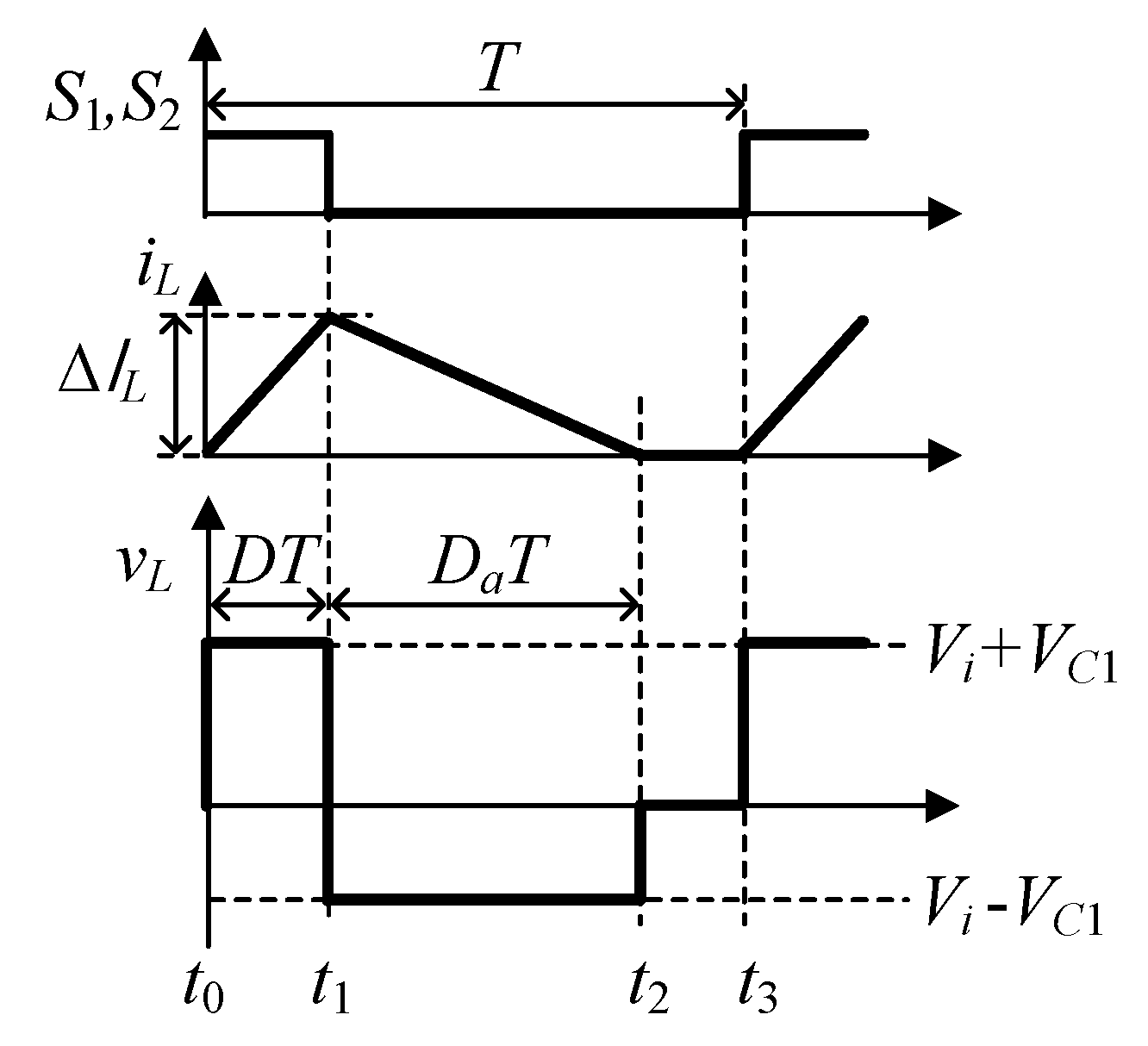
Figure 2 introduces the key waveforms of the proposed 3-SCNC type 1, where D and T are the duty cycle and the switching period. Based on the waveforms, two main operating states are defined at every switching period.
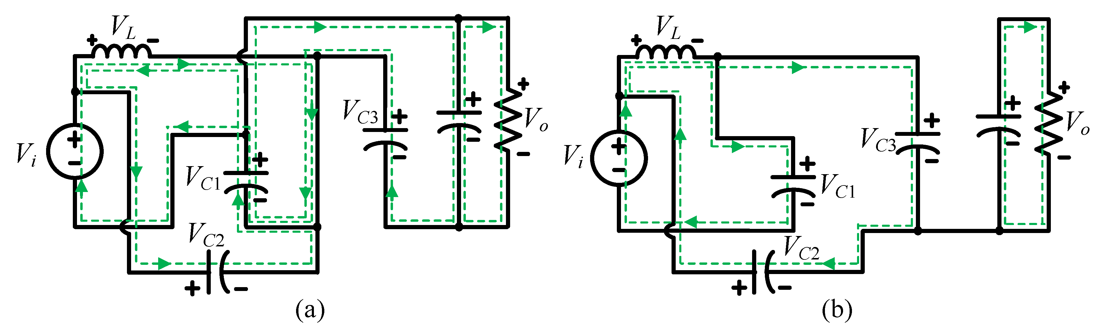
Stage 1-[t0–t1, Figure 3a]: S1 and S2 are turned on at D·T. The inductor is charged by the input DC source and the C1 capacitor, the C2 and C3 capacitors are discharged. The D1, D2, D3 and D4 diodes are reverse-biased when the D0 diode is forward-biased. The following equation is written:
Stage 2-[t1–t2, Figure 3b]: S1 and S2 are turned off at the same time (1 − D)·T; the D1, D2, D3, and D4 diodes are reverse-biased while the D0 diode is forward-biased. We have
According to the volt-second balance law of the inductor in one switching period, (1) to (2) yield the following equation:
By substituting (3) to (1), the voltage gain of the proposed 3-SCNC type 1 in the CCM is derived
2.2. Operating Principle of the Proposed 3-SCNC Type 2
Compared to 3-SCNC type 1, the proposed 3-SCNC type 2 has lower voltage stress across capacitor C2, as seen in Figure 1b. It can be created by changing the connection of capacitor C2 to DC-source. According to the PWM method in Figure 2, the equivalent circuit of the proposed 3-SCNC type 2 in CCM operation can be divided into two states, as shown in Figure 4.
When S1 and S2 are turned on, the equations are obtained
When S1 and S2 are turned off. The extra equations are given
By applying volt-second balance for the inductor, the voltage of capacitors can be expressed
By combining (5) and (7), the voltage gain of proposed 3-SCNC type 2 is obtained
2.3. Operating Principle of the Proposed 3-SCNC Type 3
Moreover, the CCM analysis of the proposed 3-SCNC type 3 is also considered with PWM method in Figure 2. The equivalent circuits are shown in Figure 5.
When switches S1 and S2 are turned on, the following equations are given
When S1 and S2 are off. The above equations can be rewritten
At steady state, based on the volt-second relationship of L, the voltage of capacitors and voltage gain are calculated as
2.4. Operating Principle of 3-SCNC Type 4
Similarly, the proposed 3-SCNC type 4 is also analyzed with two states. The equivalent circuit during state 1 is shown in Figure 6.
The voltage appears the inductor L and output voltage are given by
When S1 and S2 are turned off. The above equations can be rewritten
According to the volt-second balance law, from (12) to (13), we have
The voltage gain can be obtained as
3. DCM Boundary Condition and Influence of Parasitic Components Analysis
To simplify the analysis process of the proposed 3-SCNCs under different operation conditions, one of the proposed converters, the 3-SCNC type 1 is considered as an example. It is analyzed in detail in DCM operation and a voltage gain analysis with parasitic components is presented. Moreover, the other proposed 3-SCNC’s analyses can be determined with the same method.
3.1. DCM Derivation
For the DCM analysis, the key waveforms of the proposed 3-SCNCs in DCM are presented in Figure 7. The voltage across inductor can be written as
According to Figure 3a and (1), the peak to peak current ripple of the inductor is calculated
The average inductor current is the input current and can be determined
Based on the condition of DCM as
Substituting (17) and (18) into (19), we have the results in
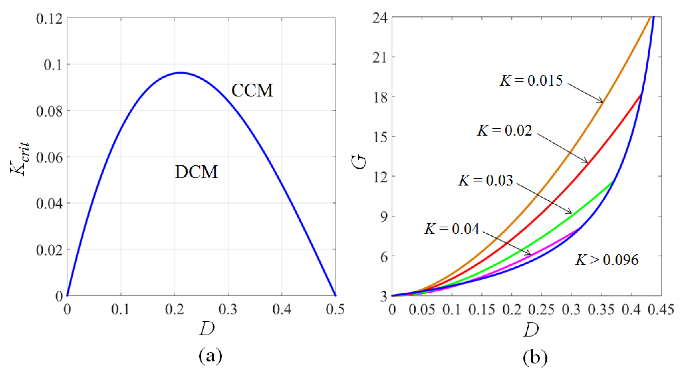
where K is a normalized coefficient to define the operation mode of the converter, and K = 9L/(2RT), Kcrit = D(1 − D)(1 − 2D).
Referring to Figure 7, the average value of inductor current is determined as follows
Apply the volt-second balance law of inductor to (16), Da can be written as
In terms of (18), (21) and (22), the output voltage gain in DCM is derived as
Figure 8a shows the plots of CCM/DCM boundary curve. Then, one can define the operation mode of the proposed 3-SCNC type 1 in CCM when K > Kcrit; otherwise the converter considers with DCM operation. Furthermore, the voltage gains of the proposed 3-SCNC type 1 in DCM are different when the values of duty cycle D and coefficient K are changed. Figure 8b shows the voltage gain in DCM with several colored curves with different D and K. When K < 0.096, the converter expresses in CCM and the voltage gain is increased as K decreases.
3.2. Voltage Gain Considering Parasitic Components
To simplify the parasitic verification, the winding resistor of the inductor, the ESR of the capacitors, the conduction resistor of the switches and the diode forward voltage are denoted by rL, rC, rS, and VD, respectively. The equivalent circuit in the conduction interval of each case are shown in Figure 9. Applying the chare-second balance principle to the capacitors, we obtain
In the duration time (1 − D)T, the capacitors C2 and C3 voltage are determined
The inductor current can be written
According to the voltage-second balance on the inductor, we have
Substituting (24)–(26) into (27), the output voltage can be rewritten
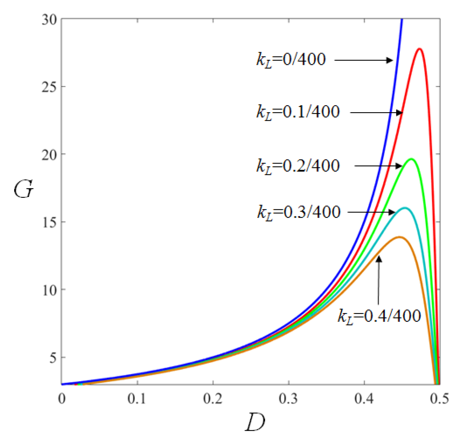
It can be seen that the voltage gain is defended on the parasitic parameters. Assuming that rL = 10rC = 6rS, kL = rL/R and VD = 0.01Vi. Figure 10 validates the relationship between the gain versus duty cycle when the resistance of the components is increased.
Where VS1/Vi and VS2/Vi are the drain-source voltage stresses of S1 and S2, respectively. VDx/Vi is the voltage stress of diodes (x is the number of diodes) and VCy/Vi is the voltage stress of capacitors (y is the number of capacitors).
4. Comparison with Other High Step-Up Transformer-Less DC-DC Converter
4.1. Voltage Gain
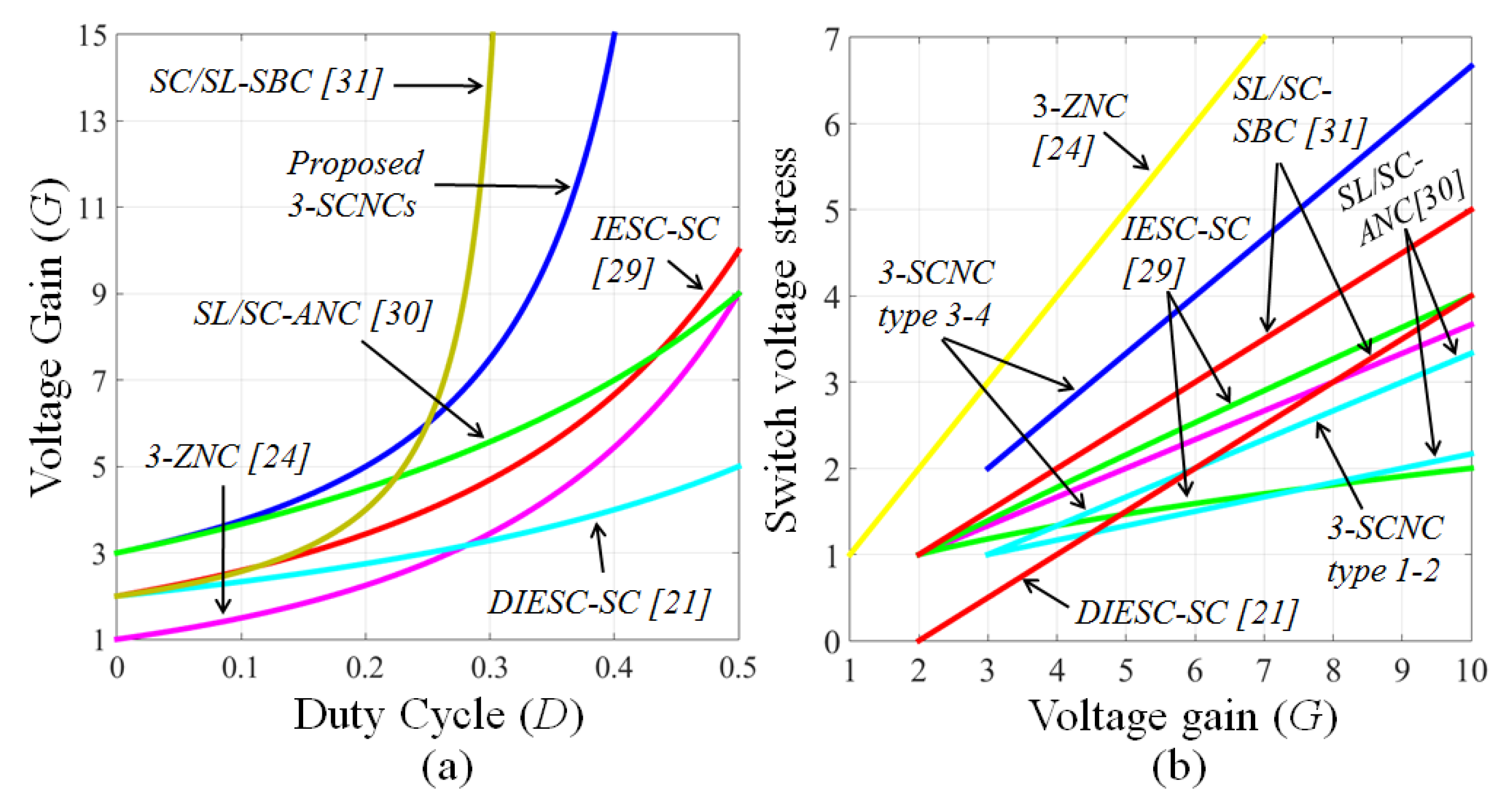
Currently, research literature is often focused on extending the boost ratio with higher efficiency, decreasing component count, consequently size, weight, losses and minimizing the stresses of component. In order to evaluate the characteristics of the proposed 3-SCNCs, the comparison between the proposed 3-SCNCs and other high step-up transformer-less DC-DC converters are summarized in Table 1. For better insight, the comparison of voltage gain versus duty cycle is plotted as shown in Figure 11a. It can be noticed that the proposed 3-SCNCs requires the lowest duty cycle for the same voltage gain than that of DIESC-SC [21], 3-ZNC [24], IESC-SC [29], and SL/SC-ANC [30]. When the duty cycle is higher than 0.25, the voltage gain of the proposed 3-SCNCs is lower than SL/SC-SBC [31]. However, the SL/SC-SBC [31] uses two more components.
4.2. The Number of Components
Compared to DIESC-SC [21] and 3-ZNC [24], the proposed 3-SCNCs use one more active switch, but reduce a large number of inductors and diodes. In addition, the total number of components used at the proposed 3-SCNCs and DIESC-SC [21] is the same, which is 12. Nevertheless, the proposed 3-SCNCs use one less inductor and capacitor. Compared with the IESC-SC [29], proposed 3-SCNCs have two less inductors, and two less capacitors. The proposed 3-SCNCs contain one more capacitor than the SL/SC-ANC [30] and SC/SL-SBC [31]. However, it has two less inductors, one less diode and one less inductor, two less diodes than that of SL/SC-ANC [30], SC/SL-SBC [31], respectively. Therefore, the size, cost, and weight of the proposed 3-SCNCs are lower than those of other converters.
4.3. Comparison of Stresses and Input Current Ripple
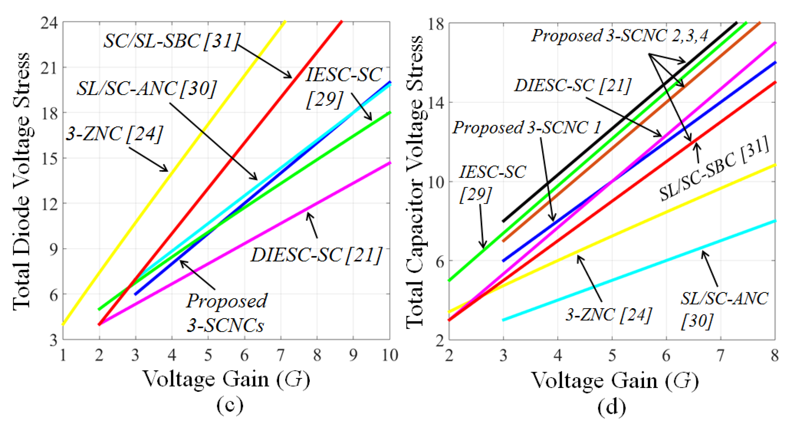
The comparison of the switch voltage stress in these nine converters is shown in Figure 11b. It can be seen that the proposed 3-SCNC type 1, 2 have lower voltage stress than the DIESC-SC [21], 3-ZNC [24], and SL/SC-SBC [26]. Besides, to produce the same output voltage gain, the proposed 3-SCNCs produce a lower switching voltage stress of the diodes than the 3-ZNC [24], SL/SC-ANC [30] and SL/SC-SBC [31], but higher than that of the DIESC-SC [21], IESC-SC [29]. From Figure 11d, it can be observed that the proposed 3-SCNC type 2 has lower capacitors voltage stress than the proposed 3-SCNC 1, 3, 4, DIESC-SC [21], IESC-SC [29], and equal SL/SC-SBC [31]. Moreover, the capacitor voltage stress of the proposed 3-SCNC type 2 has lower than DIESC-SC [21] and IESC-SC [29].
As presented in Table 1, the input current ripple comparison is also discussed. The input current ripple of the DIESC-SC [21], 3-ZNC [24], IESC-SC [29], SL/SC-ANC [30], SL/SC-SBC [31], the proposed 3-SCNC type 2 and 4 are very high. This is because the capacitor, diode or switch is directly connected to DC input voltage. Moreover, in the proposed 3-SCNC type 1 and 3, the inductor is directly connected to the DC input voltage. Thus, the input current ripple of them is low.
5. Component Selections
5.1. Inductance Selection
The proposed 3-SCNC type 1 is considered as an example to design the inductor. The inductance is selected by using the current ripple of the inductor in the interval time DT. From (1) and ΔIL ≤ x%IL, the required inductance in the CCM can be derived
5.2. Capacitance Selection
The capacitors are selected with the rated voltage as presented in Table 1. Moreover, the value of capacitance is designed based on the capacitor voltage ripple. From (24), we have:
If the peak-to-peak capacitor voltage ripple is limited by y1%, the rated capacitance of capacitors C1, C2, and C3 can be derived.
Similarly, from (24) we have
The capacitance of C0 should be calculated as
5.3. Semiconductor Devices Selection
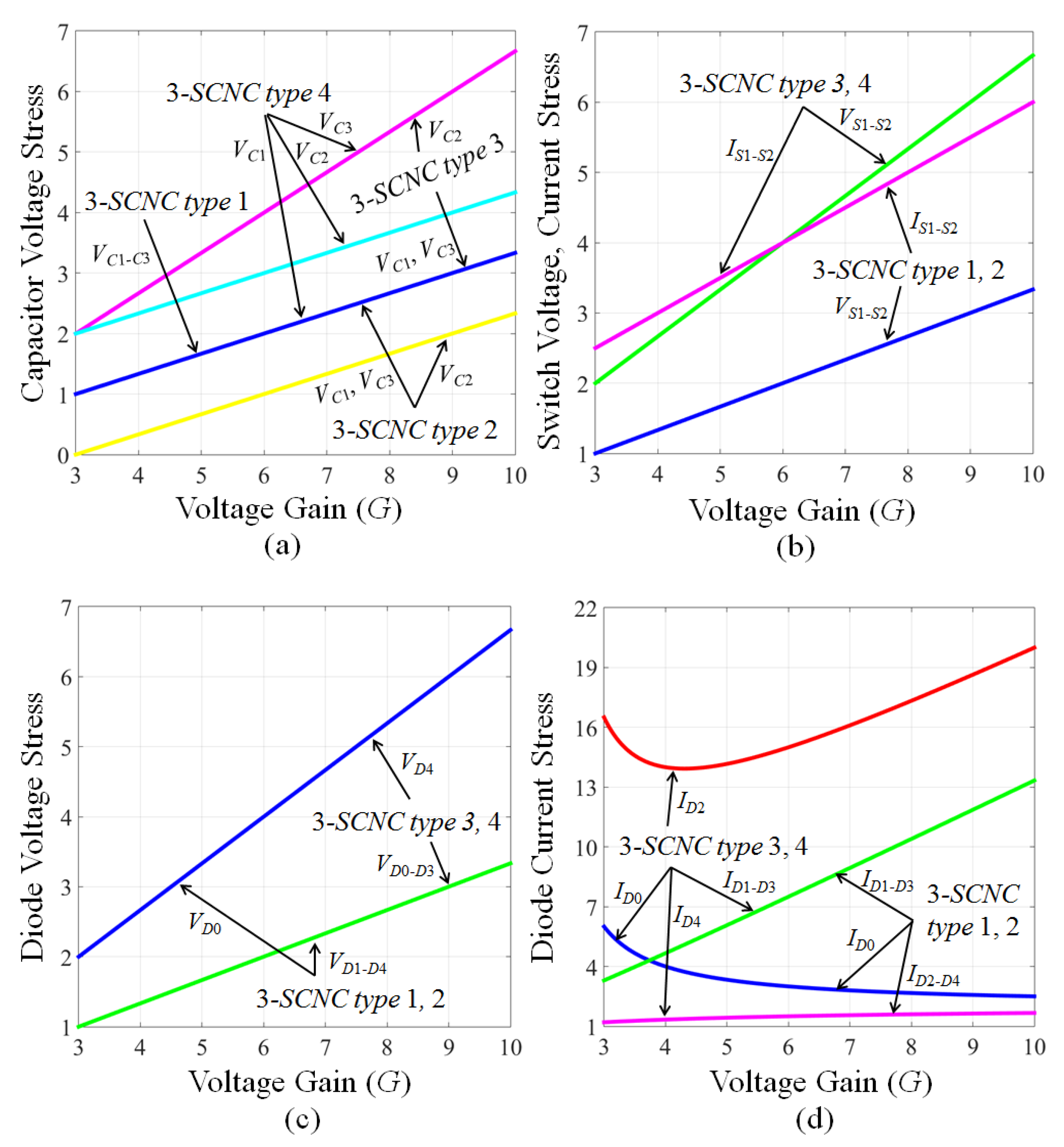
The voltage and current stresses of the proposed 3-SCNCs are the main constraint in the selection of switches and diodes to maintain them operating in their safe condition, as shown in Table 2. Moreover, the voltage and current stress comparison of the proposed 3-SCNCs for semiconductor device has been shown in Figure 12. Compared to the proposed 3-SCNC type 3-4, the proposed 3-SCNC type 1-2 has lower voltage stress of switches and capacitors.
6. Simulation and Experiment Discussion
6.1. Simulation Results
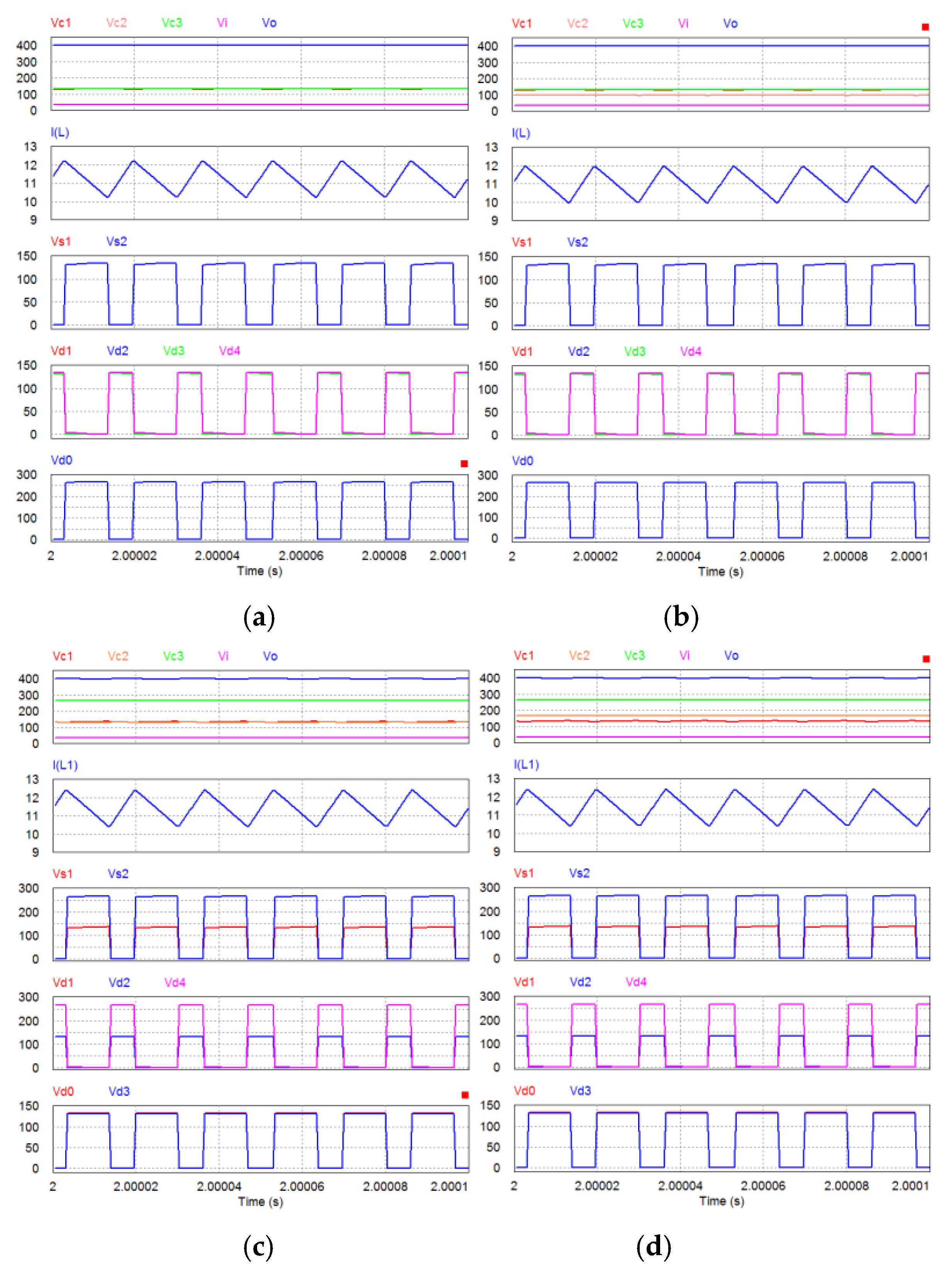
The proposed 3-SCNCs are verified by using PSIM 9.1 simulation when the input voltage and output voltage are set up 36 V and 400 V, respectively. The switching frequency is 60 kHz, and the load power is 400 W. The simulation parameters of the converters are selected as Table 3. In Figure 13, the simulation results of the proposed 3-SCNCs are shown. The voltage stress across capacitors, diodes and MOSFETs are fit well with the theoretical analysis in Table 2.
6.2. Experimental Results
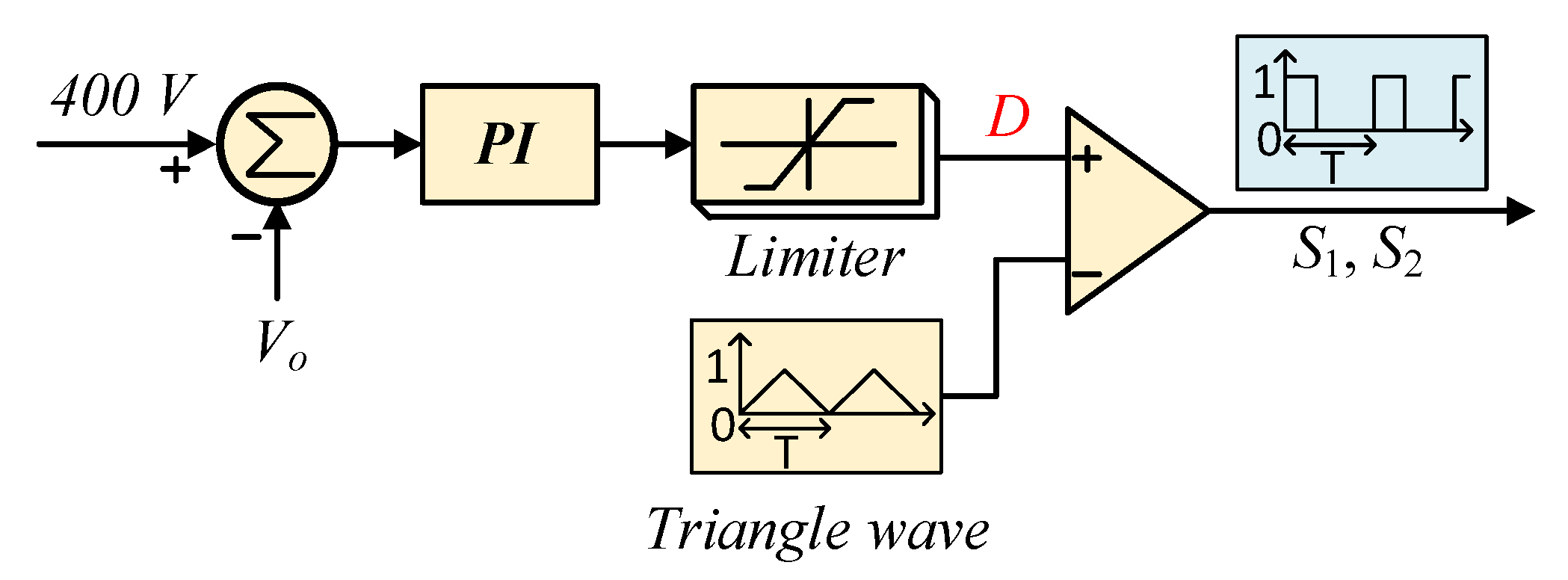
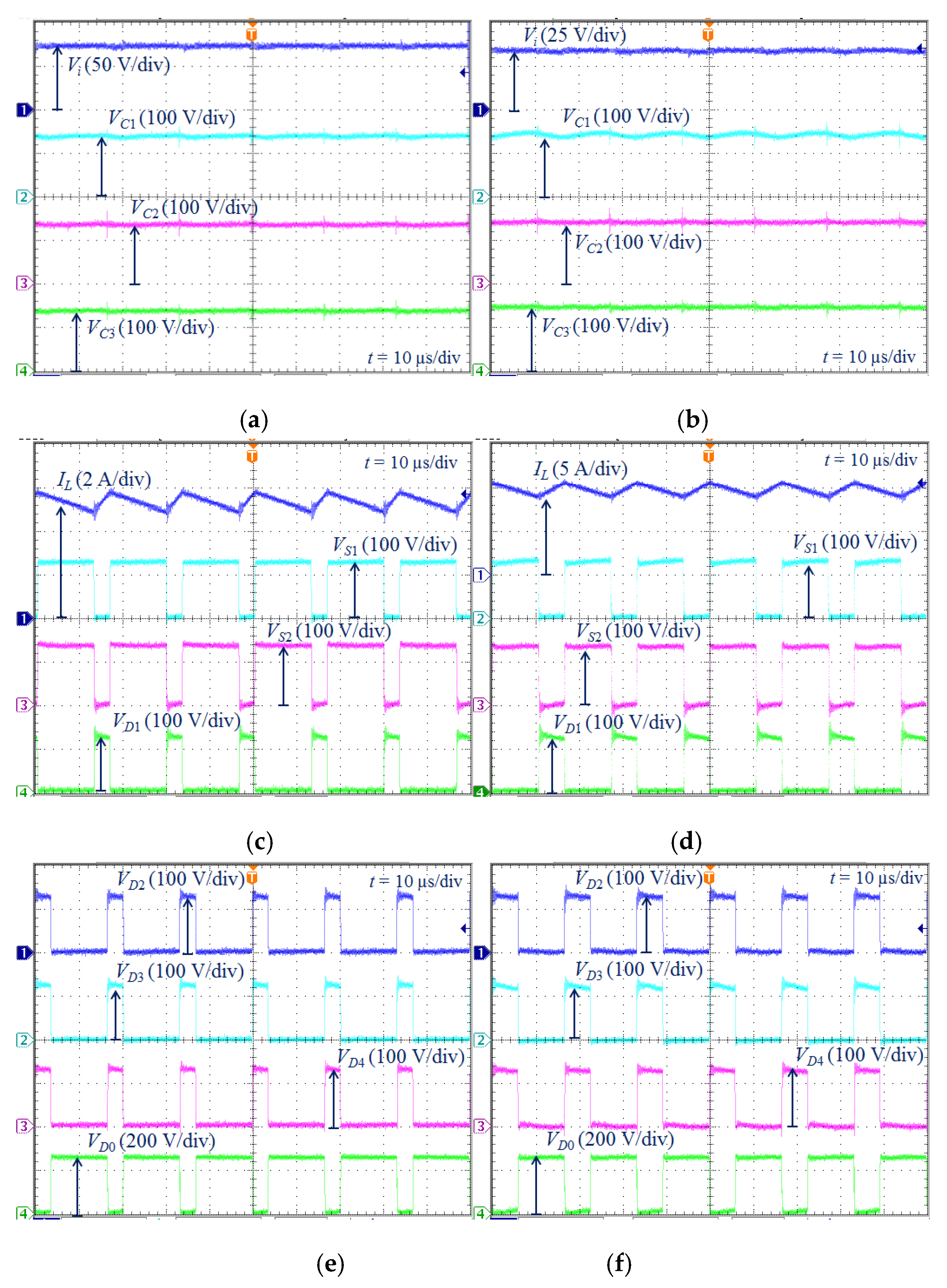
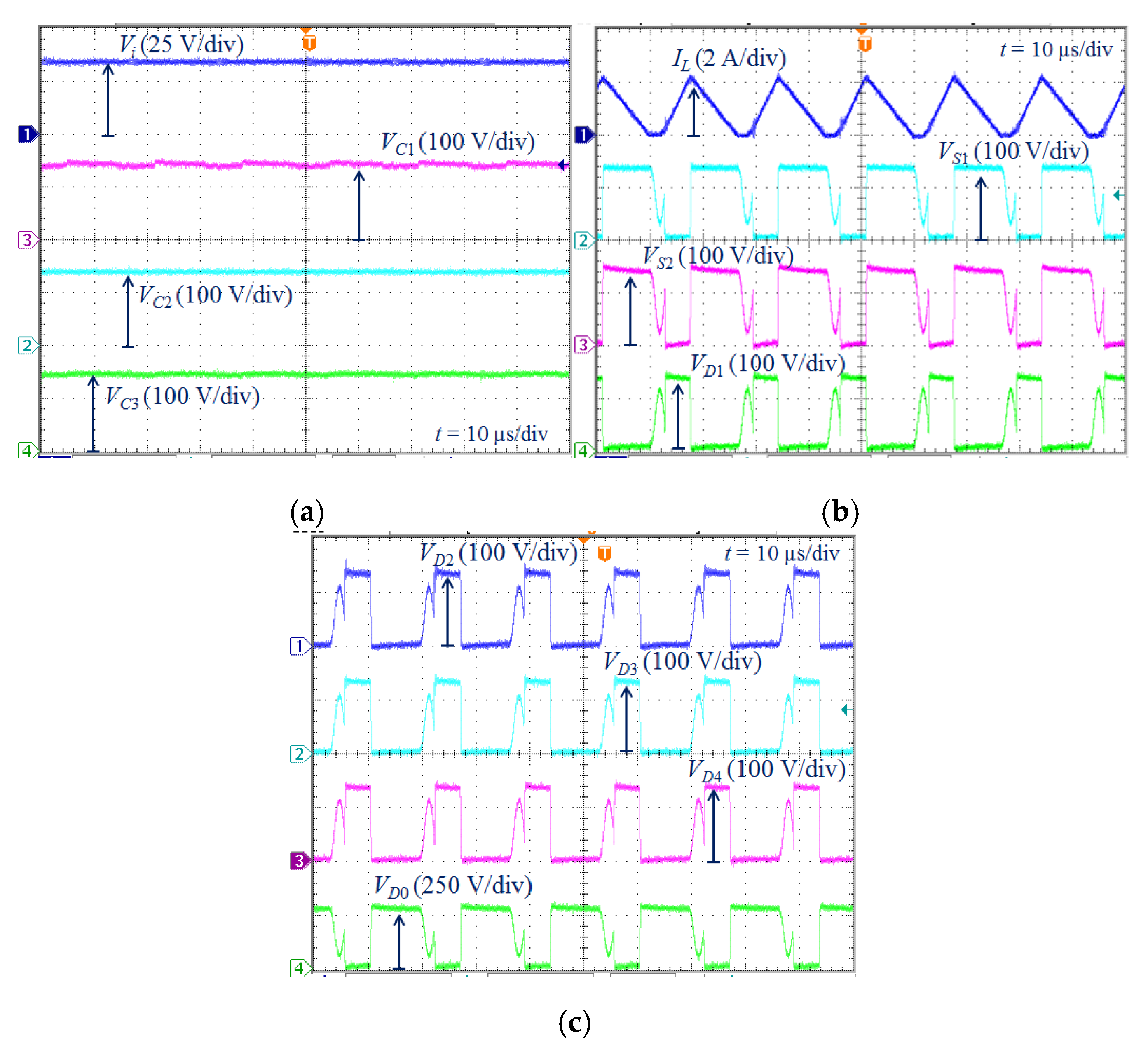
In order to verify the experimental performance of the 3-SCNCs, the laboratory prototype for proposed 3-SCNC type 1 was constructed. The main experimental parameters are selected in Table 3. Film capacitors were selected, two power switches of IRFP4668PbF MOSFETs for their low ON-resistance and four STPS60SM200C Schottky diodes were used, one more FF60UP30DN diode was used for output diode D0. While the setting parameters are applied, the converter was fed by the CHROMA 62012P-100-50 DC power supply. To maintain the output voltage at 400 V, a simple PI output voltage loop is controlled by a DSP TMS320F28335, as shown in Figure 14. Figure 15 shows the voltage waveforms of two power switches S1-S2, diodes D0-D4, capacitors C1-C3, and the current waveforms of the inductor at Po = 330 W, Vi = 72 V and Vi = 36 V. The measured values of capacitor voltage are 133.3 V each, the output voltage is 400 V. In Figure 15e,f, it is easy to see that the voltage stress of power switches S1-S2 and diodes D1-D4 are approximately the capacitor voltage. In order to verify the DCM theoretical study in Section 3.1, the experiment parameters of the proposed 3-SCNC type 1 are D = 0.3, k = 0.02, Vi = 36 V, L = 0.4 mH. The power load is decreased to 30 W in experiment. As shown in Figure 16, the capacitor C1, C2, and C3 are 134 V and 133 V. Compared to the waveforms in Figure 15 for CCM, the proposed 3-SCNC type 1 in DCM has a higher boost factor.
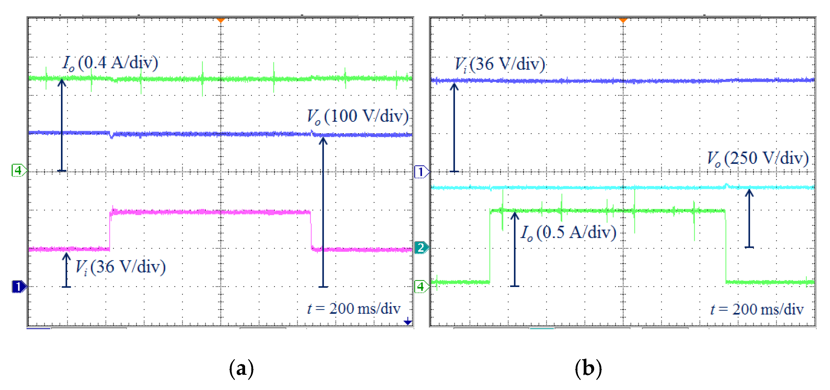
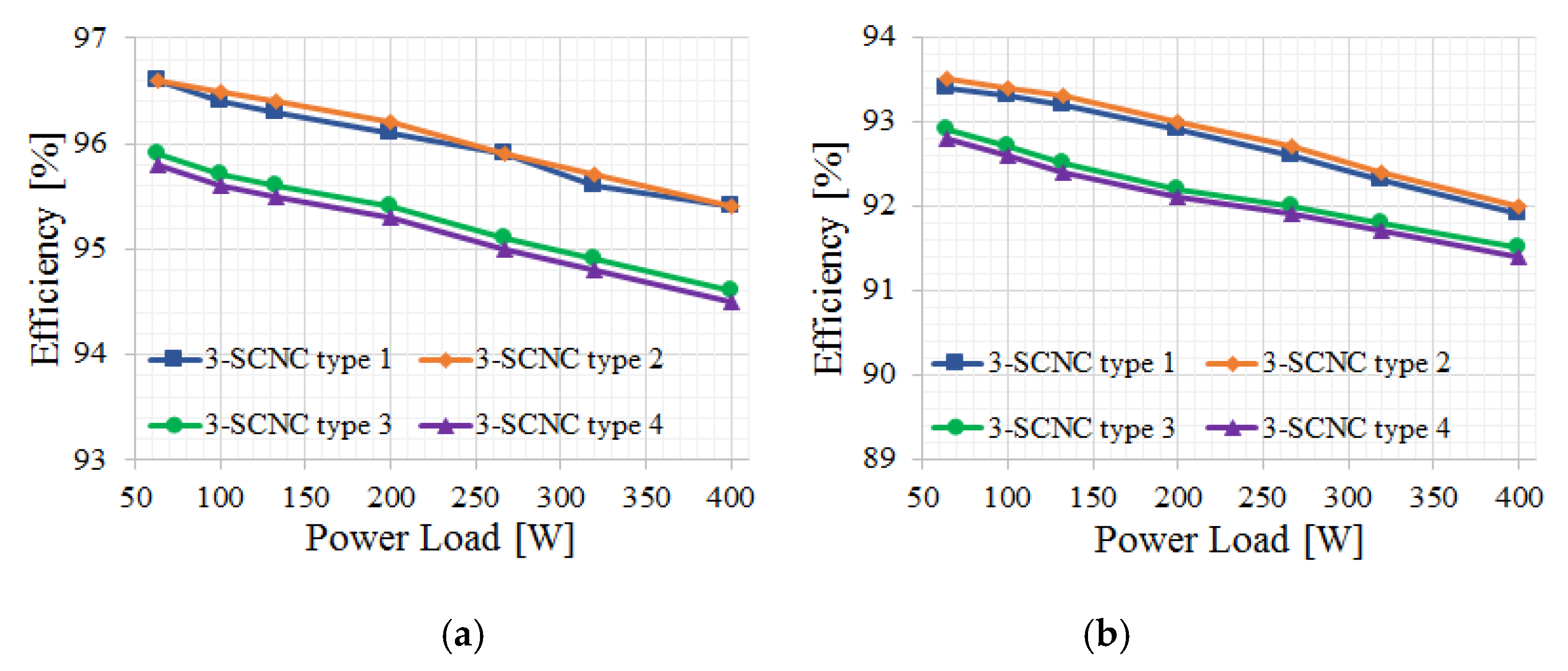
Figure 17 validates the experimental waveforms of the proposed 3-SCNC type 1 while the controller is executed. Thereby, the output reference voltage is set as 400 V and the output power is 400 W, while the input DC source is adjusted from 36 V to 72 V. In next case, the input voltage is set 36 V when power load changes from the light load (5% of full load) to full load of 400 W. Figure 18 presents the experimental efficiency of the proposed 3-SCNCs regarding load under Vi = 36 V and 72 V. The measurement both input and output power are performed by WT230 Power Meter from YOKOGAWA. It can be seen that the efficiency is reduced when the low input voltage is suggested, this is because the conduction loss on devices is high. It is obvious that the efficiency of the proposed 3-SCNC type 1 and 2 are higher than the proposed 3-SCNC type 3 and 4. Because the proposed 3-SCNC type 1 and 2 have lower voltage stress across capacitors, diodes and MOSFETs than that of proposed 3-SCNC type 3 and 4.
7. Conclusions
According to the advantages of the switched-capacitor technique, a class of high step-up transformer-less DC-DC converters with three switched-capacitor networks has been proposed in this paper. The characteristics of the proposed 3-SCNCs are as follows: providing a high voltage ratio with small duty cycle, thereby achieving low conduction loss of the power switches; and having a low voltage stress on the capacitors and power devices. The operating principle in CCM/DCM boundary condition, analysis with parasitic components and parameters design are derived in detail. In addition, the comprehensive comparison between the proposed 3-SCNCs and other transformer-less high step-up DC-DC converter topologies has been done, which highlighted the merits and drawbacks of the proposed 3-SCNCs. Finally, the simulation and experimental results with closed-loop controller are shown to verify the theoretical analysis.
Author Contributions
T.-D.D. determined topology, data analysis, and original draft preparation. M.-K.N. contributed to review and editing. T.-T.T. contributed to validating in simulation and experimental work. Y.-C.L. provided resources and supervision. J.-H.C. provided resources and funding acquisition.
Funding
This research received no external funding.
Acknowledgments
This research was supported in part by the Korea Electric Power Corporation (Grant number: R18XA04). This work was supported by the Korea Institute of Energy Technology Evaluation and Planning(KETEP) and the Ministry of Trade, Industry & Energy (MOTIE) of the Republic of Korea (No. 2019381010001B). The authors would like to thank Adrian Ioinovici for his valuable comments on this work.
Conflicts of Interest
The authors declare no conflict of interest.
References
- Abu-Rub, H.; Malinowski, M.; Al-Haddad, K. Power Electronics for Renewable Energy Systems, Transportation and Industrial Applications; John Wiley & Sons: Hoboken, NJ, USA, 2014. [Google Scholar]
- Sarvar, H.N.; Muhammad, U.A.; Zafar, A.; Sadam, H.; Tahir, M.; Muhammad, J.A.; Raghavendra, K.V.G.; Kim, H.J. An Optimized Methodology for a Hybrid Photo-Voltaic and Energy Storage System Connected to a Low-Voltage Grid. Electronics 2019, 8, 176. [Google Scholar]
- Mattia, F.; Marta, M.; Eneko, O.O. A flexible power electronics configuration for coupling renewable energy sources. Electronics 2015, 4, 283–302. [Google Scholar]
- Forouzesh, M.; Siwakoti, Y.P.; Gorji, S.A.; Blaabjerg, F.; Lehman, B. Step-up DC-DC converters: A comprehensive review of voltage-boosting techniques, topologies, and applications. IEEE Trans. Power Electron. 2017, 32, 9143–9178. [Google Scholar] [CrossRef]
- Lin, B.R. Analysis of a DC converter with low primary current loss and balance voltage and current. Electronics 2019, 8, 439. [Google Scholar] [CrossRef]
- Nguyen, M.K.; Lim, L.C.; Choi, J.H.; Cho, G.B. Isolated High Step-up DC-DC Converter Based on Quasi-Switched-Boost Network. IEEE Trans. Ind. Electron. 2016, 63, 7553–7562. [Google Scholar] [CrossRef]
- Oleksandr, H.; Tatiana, S.; Dmitri, V.; Carlos, R.C.; Enrique, R.C.; Andrii, C. Comprehensive comparative analysis of impedance-source networks for DC and AC application. Electronics 2019, 8, 405. [Google Scholar]
- Nguyen, M.K.; Duong, T.D.; Lim, Y.C.; Kim, Y.J. Isolated boost dc-dc converter with three switches. IEEE Trans. Power Electron. 2018, 33, 1389–1398. [Google Scholar]
- Nguyen, M.K.; Duong, T.D.; Lim, Y.C.; Choi, J.H. Active CDS-clamped L-type current-fed isolated DC-DC converter. J. Power Electron. 2018, 18, 955–964. [Google Scholar]
- Wu, G.; Ruan, X.; Ye, Z. High step-up DC-DC converter based on switched capacitor and couple inductor. IEEE Trans. Ind. Electron. 2018, 65, 5572–5579. [Google Scholar] [CrossRef]
- Siwakoti, Y.P.; Blaabjerg, F.; Loh, P.C. Quasi-Y-source boost DC–DC converter. IEEE Trans. Power Electron. 2015, 30, 6514–6519. [Google Scholar] [CrossRef]
- Michal, F.; Jan, M.; Branislav, H.; Michal, P. The study of the operational characteristic of interleaved boost converter with modified couple inductor. Electronics 2019, 8, 1049. [Google Scholar]
- Axelrod, B.; Beck, Y.; Berkovich, Y. High step-up dc–dc converter based on the switched-coupled-inductor boost converter and diode capacitor multiplier: Steady state and dynamics. IET Power Electron. 2015, 8, 1420–1428. [Google Scholar] [CrossRef]
- Young, C.M.; Chen, M.H.; Chang, T.A.; Ko, C.C.; Jen, K.K. Cascade Cockcroft–Walton voltage multiplier applied to transformerless high step-up DC–DC converter. IEEE Trans. Ind. Electron. 2013, 60, 523–537. [Google Scholar] [CrossRef]
- Wijeratne, D.S.; Moschopoulos, G. Quadratic power conversion for power electronics: Principles and circuits. IEEE Trans. Circuits Syst. I Reg. Pap. 2011, 59, 1967–1979. [Google Scholar] [CrossRef]
- Garcia, F.S.; Pomilio, J.A.; Spiazzi, G. Modeling and control design of the interleaved double dual boost converter. IEEE Trans. Ind. Electron. 2013, 60, 3283–3290. [Google Scholar] [CrossRef]
- Alcazar, Y.J.A.; Oliveira, D.S., Jr.; Tofoli, F.L.; Torrico-Bascope, R.P. DC–DC nonisolated boost converter based on the three-state switching cell and voltage multiplier cells. IEEE Trans. Ind. Electron. 2013, 60, 4438–4449. [Google Scholar] [CrossRef]
- Jiao, Y.; Luo, F.L.; Zhu, M. Voltage-lift-type switched-inductor cells for enhancing DC–DC boost ability: Principles and integrations in Luo converter. IET Power Electron. 2011, 4, 131–142. [Google Scholar] [CrossRef]
- Rosas-Caro, J.C.; Ramirez, J.M.; Peng, F.Z.; Valderrabano, A. A DC–DC multilevel boost converter. IET Power Electron. 2010, 3, 129–137. [Google Scholar] [CrossRef]
- Tran, V.T.; Nguyen, M.K.; Choi, Y.O.; Cho, G.B. Switched-capacitor-based high boost DC-DC converter. Energies 2018, 11, 987. [Google Scholar] [CrossRef]
- Wu, G.; Ruan, X.; Ye, Z. Nonisolated high step-up DC–DC converters adopting switched-capacitor cell. IEEE Trans. Ind. Electron. 2015, 62, 383–393. [Google Scholar] [CrossRef]
- Peng, F.Z. Z-source inverter. IEEE Trans. Ind. Appl. 2003, 39, 504–510. [Google Scholar] [CrossRef]
- Nguyen, M.K.; Le, T.V.; Park, S.J.; Lim, Y.C. A class of quasi-switched boost inverters. IEEE Trans. Ind. Electron. 2015, 62, 1526–1536. [Google Scholar] [CrossRef]
- Zhang, G.; Zhang, B.; Li, Z.; Qiu, D.; Yang, L.; Halang, W.A. A 3-Z-Network boost converter. IEEE Trans. Ind. Electron. 2015, 62, 278–288. [Google Scholar] [CrossRef]
- Nguyen, M.K.; Choi, Y.O.; Cho, G.B.; Lim, Y.C. Two-switch non-isolated step-up DC-DC converter. J. Power Electron. 2018, 18, 651–661. [Google Scholar]
- Nguyen, M.K.; Duong, T.D.; Lim, Y.C.; Kim, Y.G. Switched-capacitor quasi-switched boost inverters. IEEE Trans. Ind. Electron. 2018, 65, 5105–5113. [Google Scholar] [CrossRef]
- Nguyen, M.K.; Duong, T.D.; Lim, Y.C. Switched-capacitor-based dual-switch high-boost DC-DC converter. IEEE Trans. Power Electron. 2018, 33, 4181–4189. [Google Scholar] [CrossRef]
- Zhang, G.; Wang, Z.; Yu, S.S.; Chen, S.Z.; Zhang, B.; Iu, H.H.C.; Zhang, Y. A generalized additional voltage pumping solution (GAVPS) for high-step-up converters. IEEE Trans. Power Electron. 2019, 34, 6456–6467. [Google Scholar] [CrossRef]
- Jalilzadeh, T.; Rostami, N.; Babaei, E.; Maalandish, M. Non-isolated topology for high step-up DC-DC converters. IEEE J. Emerg. Sel. Top. Power Electron. 2019. [Google Scholar] [CrossRef]
- Tang, Y.; Wang, T.; Fu, D. Multicell switched-inductor/switched capacitor combined active-network converters. IEEE Trans. Power Electron. 2015, 30, 2063–2072. [Google Scholar] [CrossRef]
- Zhu, X.; Zhang, B.; Li, Z.; Li, H.; Ran, L. Extended switched-boost DC-DC converters adopting switched-capacitor cells for high step-up conversion. IEEE J. Emerg. Sel. Top. Power Electron. 2017, 5, 1020–1030. [Google Scholar] [CrossRef]
Figure 1.
Proposed DC–DC converters with three switched-capacitor networks (3-SCNCs): (a) Type 1, (b) Type 2, (c) Type 3 and (d) Type 4.
Figure 1.
Proposed DC–DC converters with three switched-capacitor networks (3-SCNCs): (a) Type 1, (b) Type 2, (c) Type 3 and (d) Type 4.

Figure 2.
PWM control method for the proposed 3-SCNC type 1 in CCM.

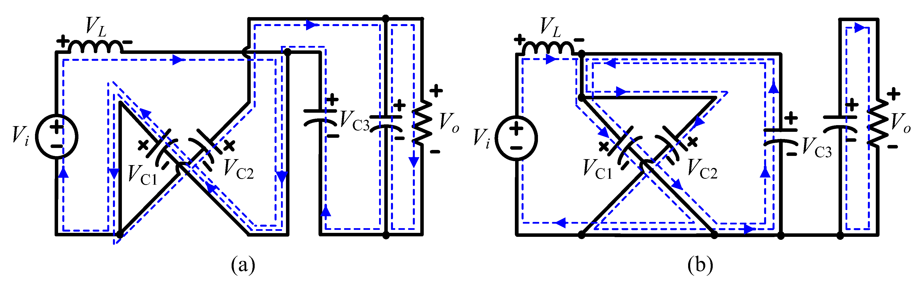
Figure 3.
Equivalent circuits of the proposed 3-SCNC type 1. (a) State 1, (b) State 2.

Figure 4.
Equivalent circuits of the proposed 3-SCNC type 2. (a) State 1, (b) State 2.

Figure 5.
Equivalent circuits of the proposed 3-SCNC type 3. (a) State 1, (b) State 2.

Figure 6.
Equivalent circuits of the proposed 3-SCNC type 4. (a) State 1, (b) State 2.

Figure 7.
Operating waveform of the proposed 3-SCNCs in DCM.

Figure 8.
Operating plot of the proposed 3-SCNC type 1: (a) CCM/DCM boundary condition. (b) Voltage gain with different K.
Figure 8.
Operating plot of the proposed 3-SCNC type 1: (a) CCM/DCM boundary condition. (b) Voltage gain with different K.

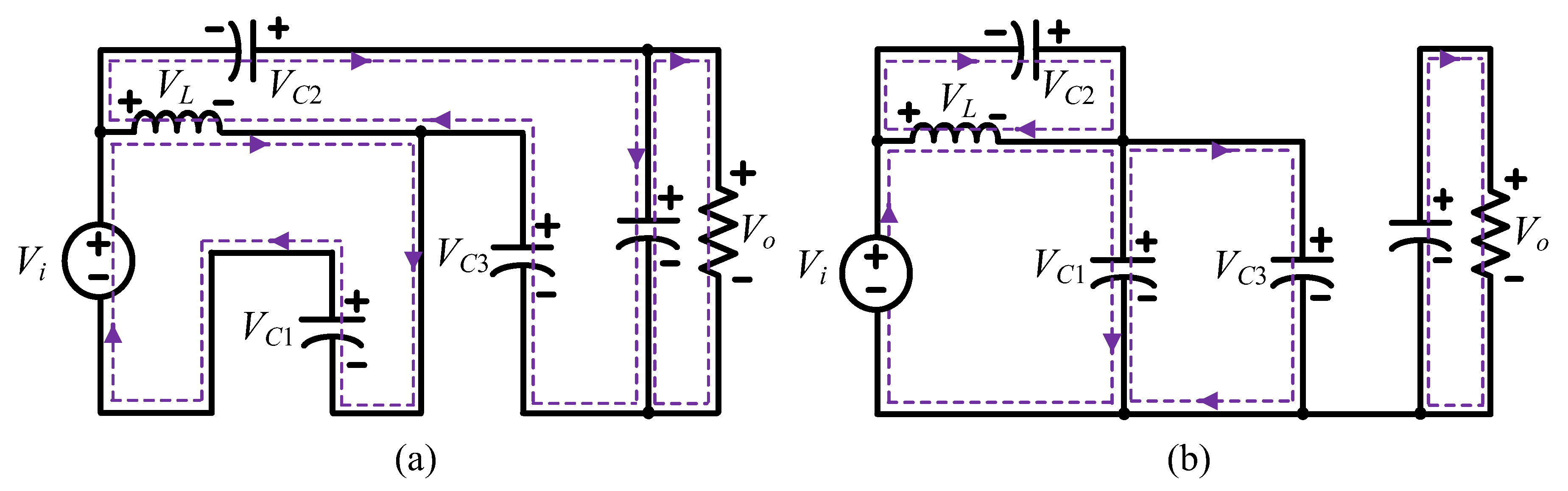
Figure 9.
Simplified circuit for parasitic components. (a) State 1, (b) State 2.

Figure 10.
The relationship between the resistance ratio rL/R and the voltage gain ratio G.

Figure 11.
Comparison of (a) Voltage gain, (b) Voltage stress of switch, (c) Voltage stress of diode, (d) Voltage stress of capacitor.
Figure 11.
Comparison of (a) Voltage gain, (b) Voltage stress of switch, (c) Voltage stress of diode, (d) Voltage stress of capacitor.


Figure 12.
Voltage and current stresses comparison of the proposed 3-SCNCs. (a) Voltage stress of capacitor, (b) Voltage and current stress of switch, (c) Voltage stress of diode, (d) Current stress of diode.
Figure 12.
Voltage and current stresses comparison of the proposed 3-SCNCs. (a) Voltage stress of capacitor, (b) Voltage and current stress of switch, (c) Voltage stress of diode, (d) Current stress of diode.

Figure 13.
Simulation results of the proposed 3-SCNCs with Vi = 36 V. (a–d) From top to bottom: capacitors C1-C2-C3 voltage, output voltage, input voltage, inductor current, voltage stress of switches S1-S2, and voltage stress of diodes D0 to D4.
Figure 13.
Simulation results of the proposed 3-SCNCs with Vi = 36 V. (a–d) From top to bottom: capacitors C1-C2-C3 voltage, output voltage, input voltage, inductor current, voltage stress of switches S1-S2, and voltage stress of diodes D0 to D4.

Figure 14.
PI voltage controller for the proposed 3-SCNCs.

Figure 15.
Experiment waveforms with Vi = 72 V (a,c,e) and Vi = 36 V (b,d,f). From top to bottom: (a,b) input voltage, capacitors C1, C2, C3 voltage; (c,d) inductor current, switch S1-S2 voltage, diode D1 voltage; (e,f) diode D2-D3-D4-D0 voltage.
Figure 15.
Experiment waveforms with Vi = 72 V (a,c,e) and Vi = 36 V (b,d,f). From top to bottom: (a,b) input voltage, capacitors C1, C2, C3 voltage; (c,d) inductor current, switch S1-S2 voltage, diode D1 voltage; (e,f) diode D2-D3-D4-D0 voltage.

Figure 16.
Experiment waveforms in DCM. From top to bottom: (a) input voltage, capacitors C1, C2, C3 voltage; (b) inductor current, switch S1-S2 voltage, diode D1 voltage; (c) diode D2-D3-D4-D0 voltage.
Figure 16.
Experiment waveforms in DCM. From top to bottom: (a) input voltage, capacitors C1, C2, C3 voltage; (b) inductor current, switch S1-S2 voltage, diode D1 voltage; (c) diode D2-D3-D4-D0 voltage.

Figure 17.
Transient experiment results. (a) Input voltage changed. (b) Load changed.

Figure 18.
Efficiency of the proposed 3-SCNCs at different output powers. (a) Vi = 72 V, (b) Vi = 36 V.
Figure 18.
Efficiency of the proposed 3-SCNCs at different output powers. (a) Vi = 72 V, (b) Vi = 36 V.


Table 1.
Comparison between the proposed 3-SCNCs and other high boost DC–DC converters.
| 3-ZNC [24] | DIESC-SC [21] | IESC-SC [29] | SL/SC-ANC [30] | SC/SL-SBC [31] | 3-SCNC Type 1 | 3-SCNC Type 2 | 3-SCNC Type 3 | 3-SCNC Type 4 | |
|---|---|---|---|---|---|---|---|---|---|
| Ind. | 4 | 2 | 3 | 3 | 2 | 1 | |||
| Cap. | 2 | 5 | 6 | 3 | 3 | 4 | |||
| Di./Sw. | 9/1 | 4/1 | 5/2 | 6/2 | 7/2 | 5/2 | |||
| Total | 16 | 12 | 16 | 14 | 14 | 12 | |||
| VS1/ViVS2/Vi | G | 1/(1 − D) | 1/(1 − D) 1/(1 − D)2 | 1/(1 − D) (1+D)/(1 − D) | 2D/(1 − 3D) G/2 | G/3 | G/3 | G/3 2G/3 | G/3 2G/3 |
| VDx/Vi | D/(1 − D), 1 2DG/(1+D) (1+D)/(1 − D) G | 1/(1 − D) | 1/(1 − D) 1/(1 − D)2 | 1 (2+D)/(1 − D) D/(1 − D) | G/2 2D/(1 − 3D) | G/3 2G/3 | G/3 2G/3 | G/3 2G/3 | G/3 2G/3 |
| VCy/Vi | (1 − D)/(1+D) G | 1/(1 − D) D/(1 − D) | 1/(1 − D) 1/(1 − D)2 D/(1 − D)2 | (1+D)/(1 − D) | 2D/(1 − 3D) G/2 | G/3 | G/3 2DG/3 | G/3 2G/3 | G/3 (2 − 2D)G/3 2G/3 |
| G | |||||||||
| ΔIin | High | High | High | High | High | Low | High | Low | High |
Table 2.
Voltage and current stresses of the proposed 3-SCNCs.
| Type 1 | Type 2 | Type 3 | Type 4 | |
|---|---|---|---|---|
| VC1/Vi | G/3 | G/3 | G/3 | G/3 |
| VC2/Vi | G/3 | 2DG/3 | 2G/3 | (2 − 2D)/(1 − 2D) |
| VC3/Vi | G/3 | G/3 | G/3 | 2G/3 |
| VS1/Vi | G/3 | G/3 | G/3 | G/3 |
| VS2/Vi | G/3 | G/3 | 2G/3 | 2G/3 |
| VD0/Vi | 2G/3 | 2G/3 | G/3 | G/3 |
| VD1/Vi | G/3 | G/3 | G/3 | G/3 |
| VD2/Vi | G/3 | G/3 | G/3 | G/3 |
| VD3/Vi | G/3 | G/3 | G/3 | G/3 |
| VD4/Vi | G/3 | G/3 | 2G/3 | 2G/3 |
| IS1/Io | (1+D)/D(1 − 2D) | (1+D)/D(1 − 2D) | (1+D)/D(1 − 2D) | (1+D)/D(1 − 2D) |
| IS2/Io | (1+D)/D(1 − 2D) | (1+D)/D(1 − 2D) | (1+D)/D(1 − 2D) | (1+D)/D(1 − 2D) |
| ID0/Io | 1/D | 1/D | 1/D | 1/D |
| ID1/Io | (2 − D)/(1 − D)(1 − 2D) | (2 − D)/(1 − D)(1 − 2D) | (2 − D)/(1 − D)(1 − 2D) | (2 − D)/(1 − D)(1 − 2D) |
| ID2/Io | 1/(1 − D) | 1/(1 − D) | (2 − D)/D(1 − 2D) | (2 − D)/(1 − D)(1 − 2D) |
| ID3/Io | (2 − D)/(1 − D)(1 − 2D) | (2 − D)/(1 − D)(1 − 2D) | (2 − D)/(1 − D)(1 − 2D) | (2 − D)/D(1 − 2D) |
| ID4/Io | 1/(1 − D) | 1/(1 − D) | 1/(1 − D) | 1/(1 − D) |
Table 3.
Parameters of the proposed 3-SCNCs.
| Parameter | Values | |
|---|---|---|
| Input DC source | 36 V–72 V | |
| Output voltage | 400 V | |
| Output power | 400 W | |
| Inductor | 0.5 mH | |
| Capacitors | C1, C2, C3 | 7.5 µF/350 V |
| C0 | 45 µF/450 V | |
| Switching frequency | 60 kHz | |
© 2019 by the authors. Licensee MDPI, Basel, Switzerland. This article is an open access article distributed under the terms and conditions of the Creative Commons Attribution (CC BY) license (http://creativecommons.org/licenses/by/4.0/).
Share and Cite
MDPI and ACS Style
Duong, T.-D.; Nguyen, M.-K.; Tran, T.-T.; Lim, Y.-C.; Choi, J.-H. Transformerless High Step-Up DC-DC Converters with Switched-Capacitor Network. Electronics 2019, 8, 1420. https://doi.org/10.3390/electronics8121420
AMA Style
Duong T-D, Nguyen M-K, Tran T-T, Lim Y-C, Choi J-H. Transformerless High Step-Up DC-DC Converters with Switched-Capacitor Network. Electronics. 2019; 8(12):1420. https://doi.org/10.3390/electronics8121420
Chicago/Turabian StyleDuong, Truong-Duy, Minh-Khai Nguyen, Tan-Tai Tran, Young-Cheol Lim, and Joon-Ho Choi. 2019. "Transformerless High Step-Up DC-DC Converters with Switched-Capacitor Network" Electronics 8, no. 12: 1420. https://doi.org/10.3390/electronics8121420
Note that from the first issue of 2016, this journal uses article numbers instead of page numbers. See further details here.