Low-Power RTL Code Generation for Advanced CNN Algorithms toward Object Detection in Autonomous Vehicles


DA-lab, Electrical and Computer Engineering, 3301 South Dearborn Street, Siegel Hall, Illinois Institute of Technology, Chicago, IL 60616, USA
*
Authors to whom correspondence should be addressed.
†
These authors contributed equally to this work.
Electronics 2020, 9(3), 478; https://doi.org/10.3390/electronics9030478
Submission received: 1 February 2020
/
Revised: 10 March 2020
/
Accepted: 10 March 2020
/
Published: 14 March 2020
(This article belongs to the Special Issue In-Vehicle Networking/Autonomous Vehicle Security for Internet of Things/Vehicles)
Abstract
:In the implementation process of a convolution neural network (CNN)-based object detection system, the primary issues are power dissipation and limited throughput. Even though we utilize ultra-low power dissipation devices, the dynamic power dissipation issue will be difficult to resolve. During the operation of the CNN algorithm, there are several factors such as the heating problem generated from the massive computational complexity, the bottleneck generated in data transformation and by the limited bandwidth, and the power dissipation generated from redundant data access. This article proposes the low-power techniques, applies them to the CNN accelerator on the FPGA and ASIC design flow, and evaluates them on the Xilinx ZCU-102 FPGA SoC hardware platform and 45 nm technology for ASIC, respectively. Our proposed low-power techniques are applied at the register-transfer-level (RT-level), targeting FPGA and ASIC. In this article, we achieve up to a 53.21% power reduction in the ASIC implementation and saved 32.72% of the dynamic power dissipation in the FPGA implementation. This shows that our RTL low-power schemes have a powerful possibility of dynamic power reduction when applied to the FPGA design flow and ASIC design flow for the implementation of the CNN-based object detection system.
1. Introduction
Among the machine learning algorithms, the convolutional neural network (CNN) model is one of the popular architectures and keywords at present. Technology trends indicate that deep learning algorithms are becoming the essential feature of Internet of Things (IoT) devices including autonomous vehicles. Some of these devices have limited power resources, especially the electric vehicles; thus, an energy-aware system is indispensable, due to the limited battery capacity. In particular, CNN includes other neural network models such as recurrent neural networks (RNN) and deep neural networks (DNN). These two have been used for the recognition systems in the computer vision, video processing, and image processing research areas [1,2,3,4,5,6]. Being similar to the human brain’s operation in perception and recognition, the neural network algorithms are able to process given visual information to recognize the object that we target or to predict the next movement of the target object [7,8,9,10]. The common feature of these neural network models is that they require abundant computational resources. In order to increase the computational capability, we need to extend several hardware resources including memory capacity, hard drive size, and microcontroller capability, which can process the larger amount of data simultaneously or in parallel. This increased hardware capability causes a large amount of power consumption inevitably. Consequently, if we reduce the power consumption of the system, naturally, we can reach the conclusion of the degradation of the computational ability of the entire system [11]. Since deep learning is widely applied, the field-programmable gate array (FPGA) has become the solution for power-efficient hardware platforms. FPGA has been getting attention as an extensible computational device. It has also become known as a device that consumes less power than the graphics processing unit (GPU) [7,8,9,10,12].
With the growing usage of CNN-based Internet of Thing (IoT) products, including autonomous vehicles, companies are developing and releasing various sizes of customized chips to support the massive amount of CNN computational processes, such as the Tensor Processing Unit (TPU), deep learning processing unit (DPU), holographic processing unit (HPU), image processing unit (IPU), neural network processing unit (NPU), and vision processing unit (VPU) [13]. In the ASIC design flow, there are opportunities to minimize and optimize those chips for high-performance and redundant power reduction. The compact size, high-speed processing, energy-efficient design, and powerful parallel computing are the primary features of the artificial intelligence (AI) accelerator chip. However, in the case of the compact size chip design, excessive power dissipation leads to increased board temperature and cooling cost, as well as potential reliability problems [14].
The implementation process is composed of the CNN architecture, the CNN accelerator, an efficient coding technique, and the hardware material to implement the power-efficient deep learning algorithm. In terms of the power dissipation for the hardware itself, we can approach primarily two aspects, which are the hardware material aspect and software architecture/algorithm model aspect. For instance, for the algorithm model aspect, to achieve high-performance and high-throughput results, most researchers and developers have suggested novel CNN architectures and efficient memory structures to decrease the processing time and improve the parallel computing performance so that they can increase the power efficiency [15,16,17,18].
In terms of hardware, the major elements that can cause a large power consumption are memory size, memory processing architecture, and the capability of parallel processing. For example, if the memory size increases, the circuit size arranged for the memory has to be increased inevitably. Consequently, longer processing time, high performance, and high integration density can cause more heat and lead to consuming more power. Due to the limitations of technology evolution in terms of the semi-conductor size, production cost, market needs, and issues in the developing process, we focus on the other elements of the hardware design flow. Traditionally, as one of the hardware level designs, register-transfer-level (RT-level) optimization is an effective methodology to reduce the dynamic power consumption of the system. Therefore, in this article, we describe the RT-level low-power techniques we demonstrated in our previous paper [19,20,21] and how to apply them to the real industry model used for real-time object detection. We evaluate the power consumption through a reliable experimental environment including an FPGA platform and ASIC design flow.
2. Background
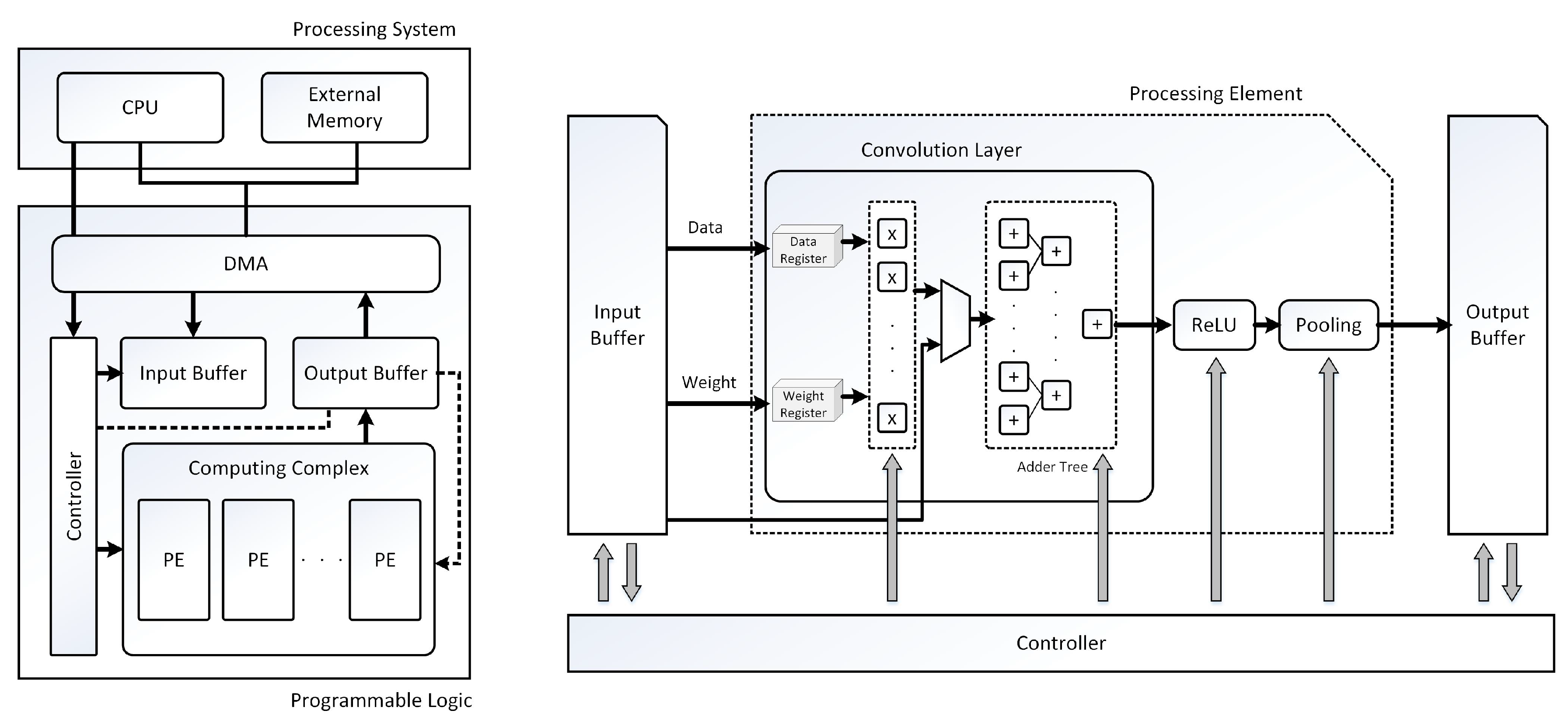
For edge computing, to overcome the lack of computational resources, researchers have analyzed the CNN computation process and developed various methodologies. The following various optimizing and accelerating methodologies focus on the performance, such as high accuracy, reduced processing time, maximized throughput, and relatively increased power efficiency. This background section shows that our experiment is an untried methodology using industrial CNN codes. Our target CNN architecture is the basic architecture, which consists of multiple interconnected convolution layers that are organized as shown in Figure 1.
Between computational convolution layers, the real computing process is affected by the loading and storing process with the internal/external data storage unit. The work in [22] proposed an energy-aware accelerator design to achieve high performance without degradation. According to this article, the crucial power issues were caused by the data transformation process. Especially, much computing resource was used for the convolution operation.
Figure 2 shows the basic data processing flow of the convolutional neural network. Typically, it is composed of hierarchically interconnected multiplication units and adder units. From the software developers’ and algorithm researchers’ perspective, the multiplication units and adder units degrade the processing speed even though they make a drastic cut of the convolution size and a number of layers before reducing or optimizing the data transformation process. Thus, they started studying the methodologies for the optimization of the data access process and extending the buffer size, developing an efficient floating point. Y.Ma et al. proposed minimized data flow to enhance the throughput [23]. D. Nguyen et al. proposed a fully pipelined convolution layer to achieve the enhanced hardware utilization [24]. This methodology was used to minimize the external data access with DRAM so that the DRAM power dissipation would decrease. In addition, there are various methodologies to improve the throughput, processing time, and power efficiency [7,8,9,10,25]. These articles introduced the methods in terms of the optimized kernel size, fixed-point arithmetic, vectorized convolutional operation, batch normalization, data scaling, etc. [16,26,27]. Recently, using an FPGA SoC board, the implementation of the CNN-based object detection system was the most fascinating method in the industrial and academic areas due to the flexibility of the implementation and evaluation [25]. Most of the FPGA products provide a high-level synthesis (HLS) design tool, which can help to create the RT-level from a behavioral description of the hardware by using well-known programming languages such as the C programming language. HLS requires the high-level and functional description of a design so that the RTL implementation can be released and automatically compiled [7,8,9,10]. FPGA products provide design tools: Xilinx provides the Vivado HLS tool; Intel provides the OpenCL Board Support Package [28,29]. At the RT-level, in addition, the developer is able to rearrange the processing schedule, reconfigure the circuit integration, and reconstruct the circuit logic elements for power reduction. A representative low-power technique is the clock gating technique [20]. Y. Chen et al. discovered the power breakdown factors of the chip running layer in each convolution layer. They said that the clock network took more than 32.9% of the entire power consumption amount. As a previous work, this article showed that the conventional clock gating technique was capable of applying the different hardware platforms, the convolution computation, and the virtual memory reconfiguration [30]. In Section 2.1, Section 2.2, Section 2.3, Section 2.4, Section 2.5 and Section 2.6, the detailed techniques will be introduced. This article will show the implementation of each technique on the FPGA hardware platform designed for the CNN-based accelerator.
2.1. Clock Gating
Clock gating is a technique to enhance performance and efficiency by eliminating unnecessary clock cycles. For example, clock gating can be achieved by selectively stopping the clock in cases when the calculation to be performed in the next clock cycle is duplicated. That is, the clock signal is either enabled or disabled depending on the idle condition of the logical network. Many CNN circuits introduced in recent years have a standby state due to the CNN characteristic and a large number of unnecessary clock cycle occurrences. Therefore, unnecessary clock cycles can be avoided with this technique, and this can prevent significant power consumption.
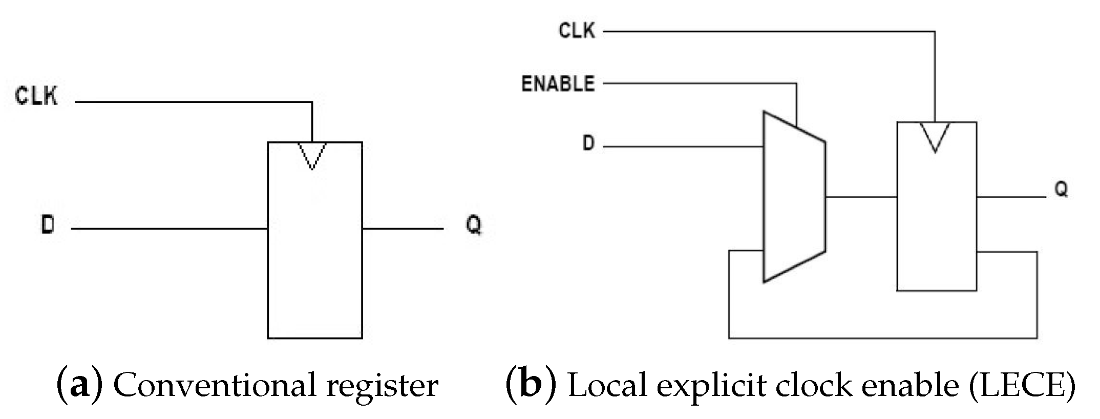
2.2. Local Explicit Clock Enable
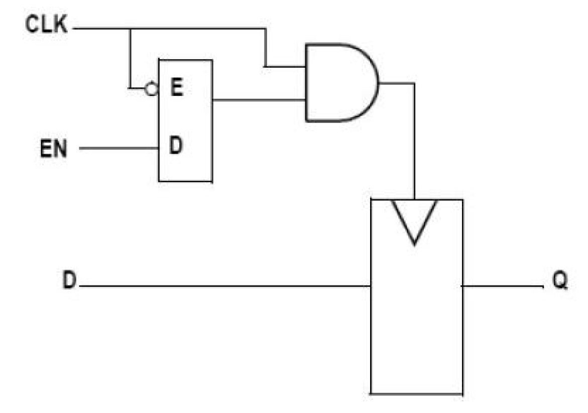
Figure 3 shows two types of registers with and without an enable signal. Furthermore, Figure 3b represents a local explicit clock enable (LECE) [19,20,21]. The output Q is updated on the rising edge of the clock only when the ENABLE signal is high. Typically, logic synthesis will implement the circuit shown in Figure 3b with a 2:1 multiplexer or a multiplexed D flip-flop if there is one available in the target technology. If the enable signal is low for a significant amount of the circuit operation and if input D and output Q are multi-bit buses, then a substantial amount of power dissipated by the clock driver is wasted. That is, driving the clock to this register when the ENABLE signal is low does not change the circuit behavior. An alternative method to implement this circuit is applying the gate on the clock (CLK). Replacing the clock input to the flip-flop with an AND gate where the inputs are the CLK and the ENABLE is not a recommended method to reduce power consumption. Considering the situation when the CLK is high and transitions occur on the ENABLEs, edges will appear on the register clock input, causing incorrect circuit behaviors. To avoid these edges, a latch must also be inserted so that when the CLK is high, no activity on the ENABLE will be transferred to the clock input. Figure 4 illustrates the additionally required circuitry.
2.3. Local Explicit Clock Gating
The schematic shown in Figure 4 describes the local explicit clock gating (LECG) technique [19,20,21]. The output Q is updated on the rising edge of the CLK, but only when the ENABLE is high. Depending on the clock insertion technique, there are two implementation methods for the LECG technique. In most cases, the physical clock insertion software will limit the choice of gates that can be used for the logic implementation. For example, a special clock gate may be needed or the tool may require insertion of a gate with the correct drive strength. In this case, the RTL design must be modified to instantiate the required gates. In some cases, it may be possible to simply write the required functionality in RTL and allow the synthesizer to select the needed gates.
2.4. Bus-Specific Clock Gating
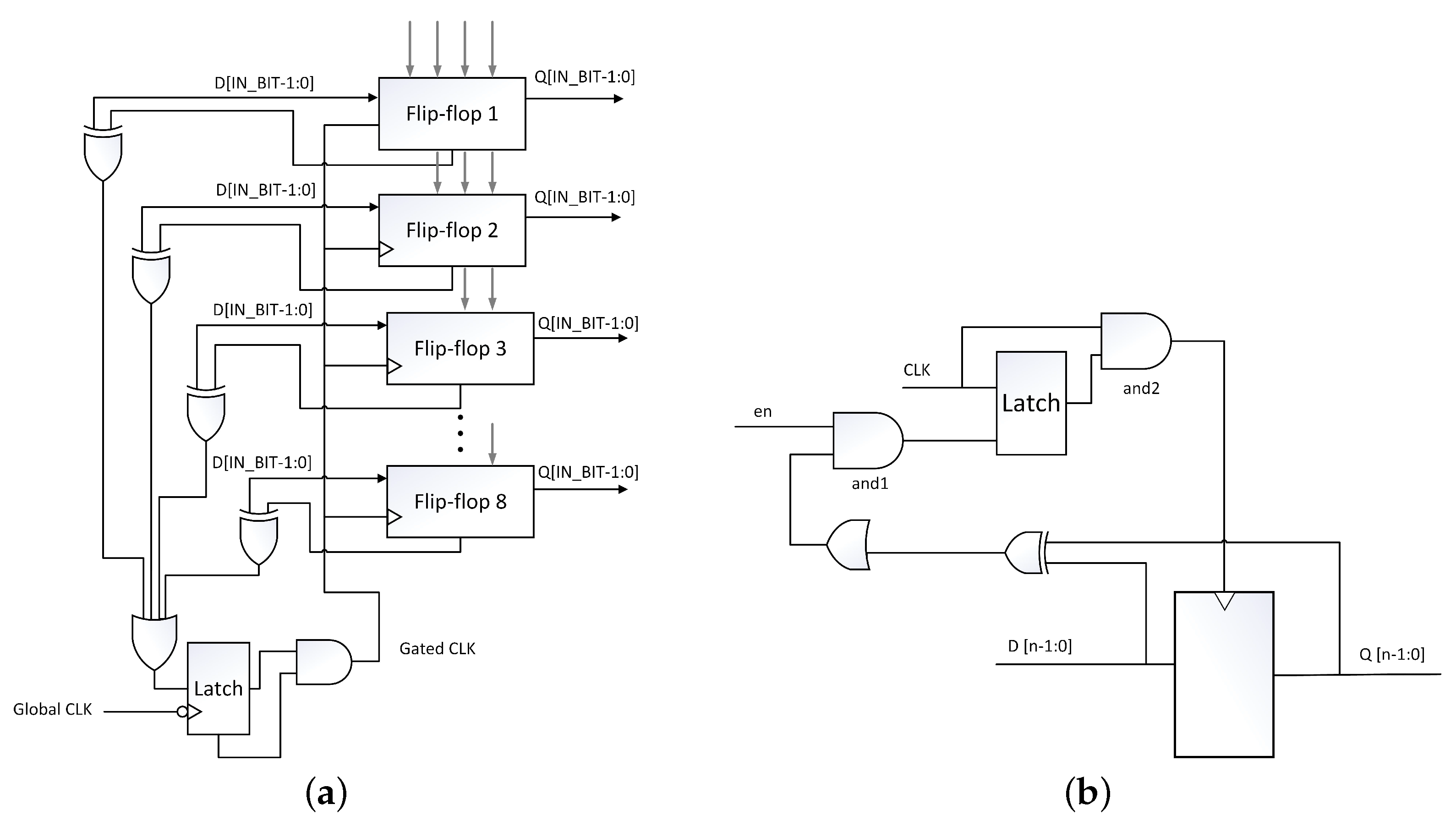
Based on the comparison of I/O signals, the bus-specific clock gating (BSCG) technique [19,20,21] utilizes the clock gating technique and adjusts the EN signal as shown in Figure 5a. The previously introduced LECE technique can deactivate blocks that are unnecessarily active, thus allowing each block to be controlled in a low-power scenario. It also filters floating signals to provide a stable signal for switching of each block. When processing a large number of bits at once, all bit lines on the data bus change state and consume redundant power. Therefore, the technique can set the active bit and reduce power to the data bus using the active bus.
2.5. Enhanced Clock Gating
The clock power of sequential logic circuits accounts for a significant portion of the total power consumption. In addition, XOR gates, compared to AND/OR gates, are significantly lower power consuming logic gates for the gate-level power analysis [19,21]. Therefore, it is effective to utilize the XOR gate in clock gating techniques, considering multi-bit I/O data, as shown in Figure 5b. In this technique, the larger pipeline level or the larger the I/O bit size, the greater the power reduction effect.
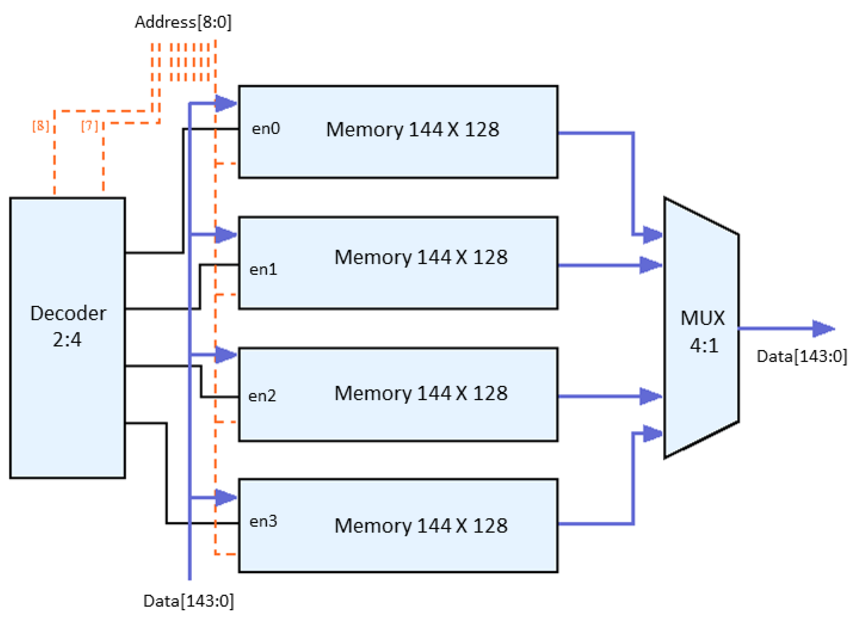
2.6. Memory Split
This technique reduces power by dividing an entire memory into several smaller memories using an output multiplexer [21]. As an example, the following Figure 6’s circuit diagram shows how power reduction can be achieved by splitting the existing 512 bytes of memory into four 128 bytes and controlling each 128 bytes’ memory block through the decoder and multiplexer.
In most of the memory block structures, half or small memory block sizes use less power than full size memory block for reading and writing operations. However, to achieve this small size of memory block, various preliminary investigations are required to determine the optimal number of memory block configurations and the memory block size. In our proposed memory structure, even if there is an identical number of reads and writes, the operation is performed only in one of the small memory blocks, instead of the full size memory, which reduces the amount of power.
3. CNN Accelerator Industrial Model: Low-Power RTL Approach
3.1. Proposed CNN Accelerator
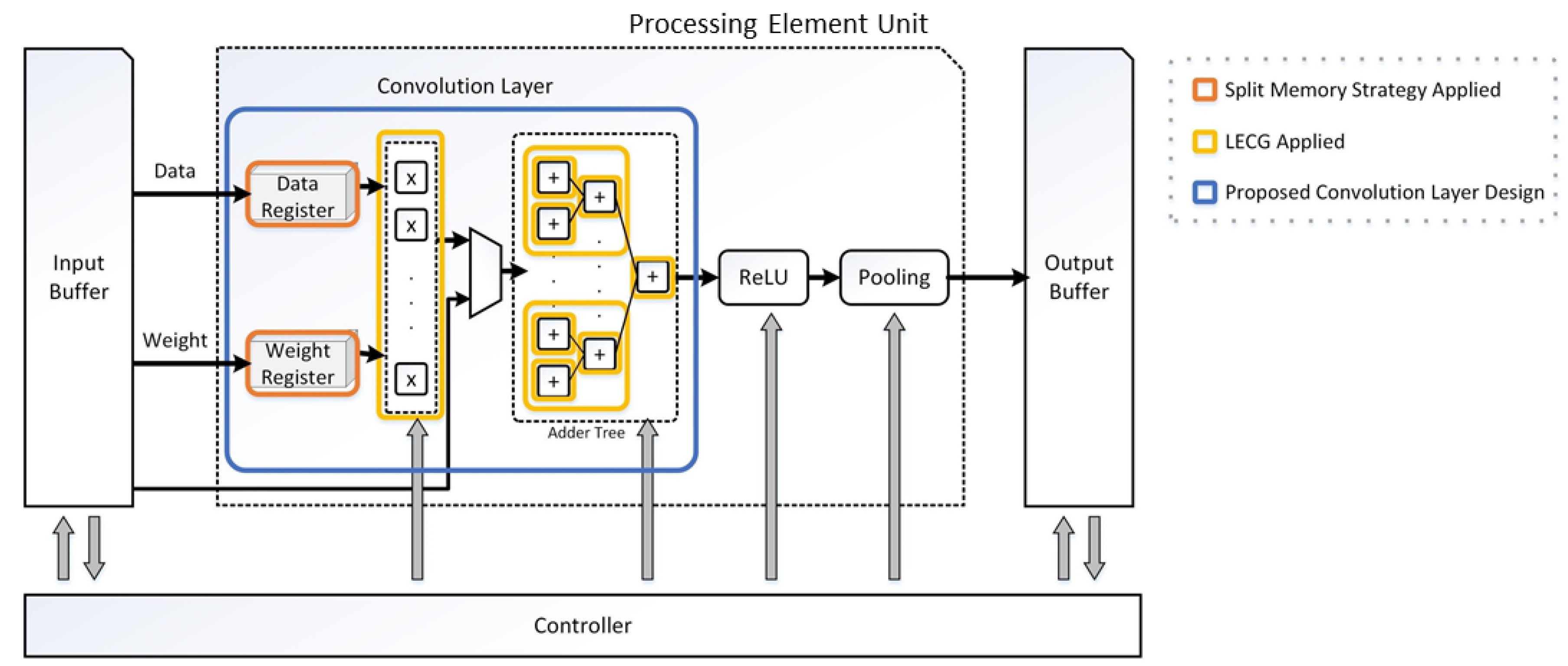
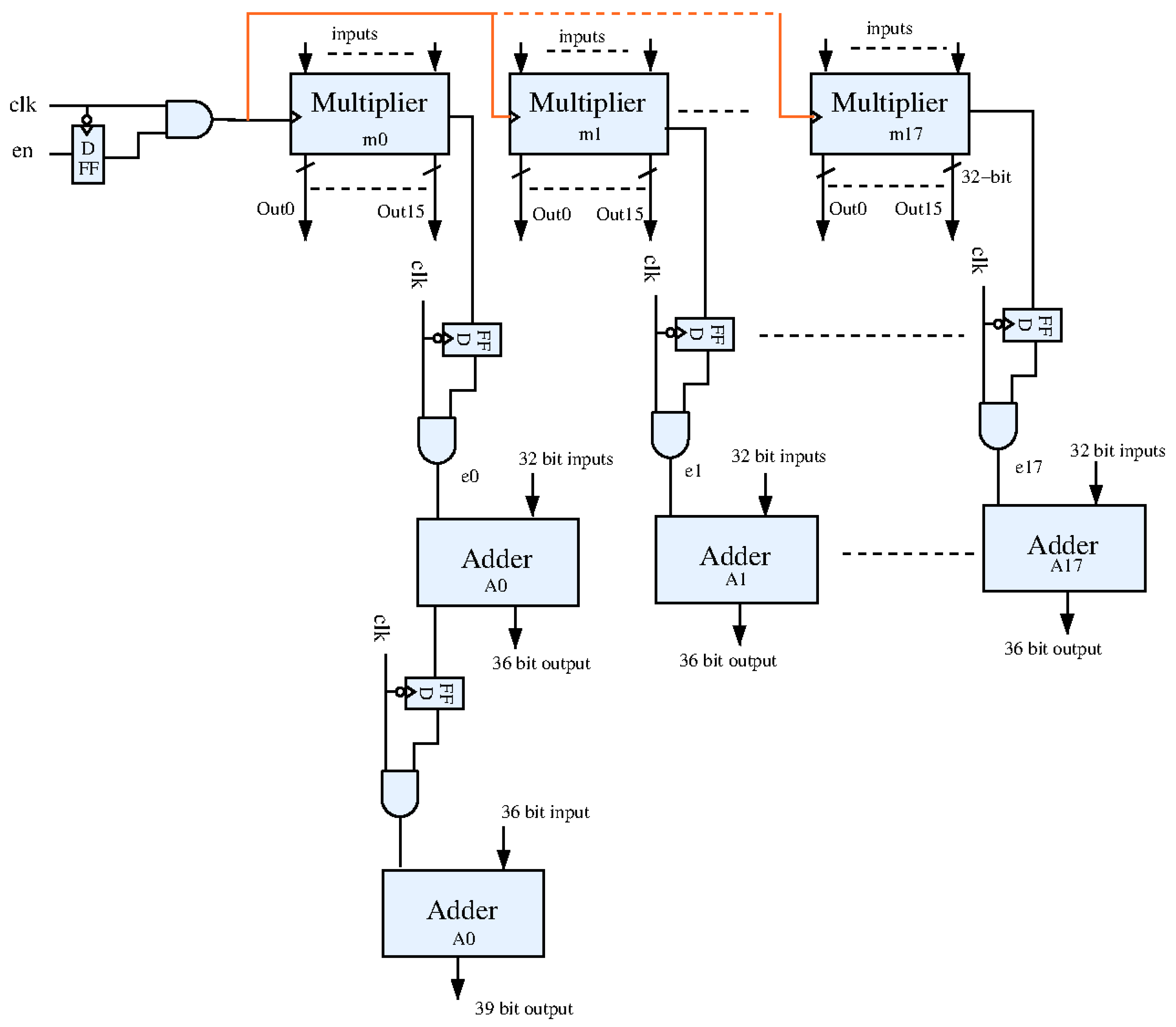
Our target was to achieve maximum power reduction by applying our proposed low-power techniques without significantly changing the conventional layer of the CNN accelerator structure. The CNN accelerator was the most frequently used part in the system for the object detection, thus consuming the most power during the detection process. In this CNN accelerator, as shown in Figure 7, we reduced power consumption by reconstructing the convolution layer part, which occupied the most part of the CNN accelerator. In Figure 7, we applied the LECG technique described in the previous section to control the multiplier and adder blocks needed for convolution, as well as to maximize the power savings by controlling the data and weight inputs through the memory split technique.
3.2. Practical Application of the Industrial CNN Accelerator
Adder and multiplier blocks were the crucial components in the CNN accelerator including the core processing element (PE) blocks. Furthermore, they were the core blocks in terms of power consumption. The convolution was performed using multiplication and additions.
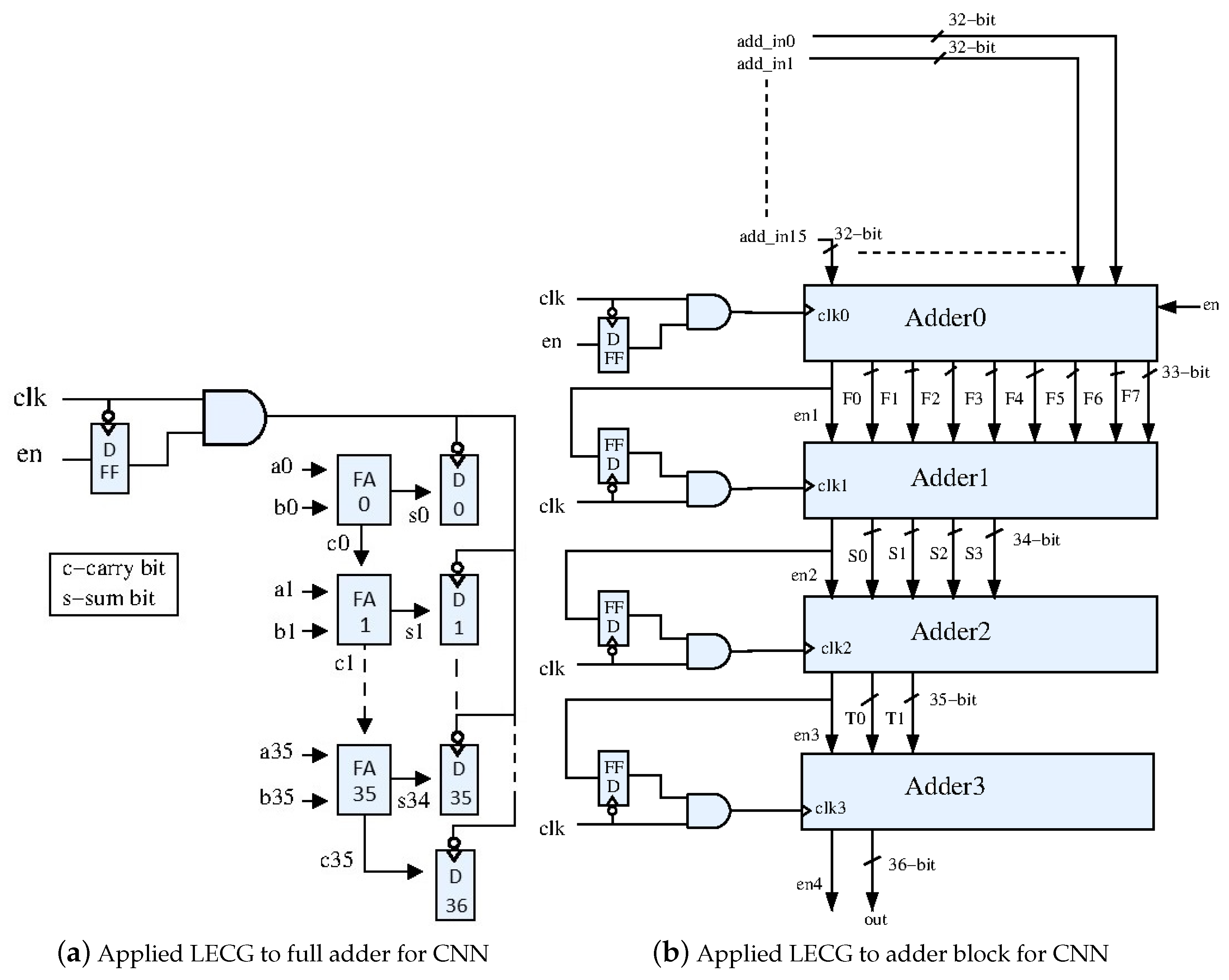
This CNN accelerator that we used as our original model utilized 32 bit adders and 36 bit adders. This design used 16 multipliers, and each had a 16 bit input and a 32 bit output. In this way, the multiplier used the 32 ×16 bit D flip flop to store the output results. We employed the clock gating to reduce the total dynamic power from these registers, as shown in Figure 8. The basic adder block also used many D flip flops, and we reduced the dynamic power by clock gating as shown in Figure 9.
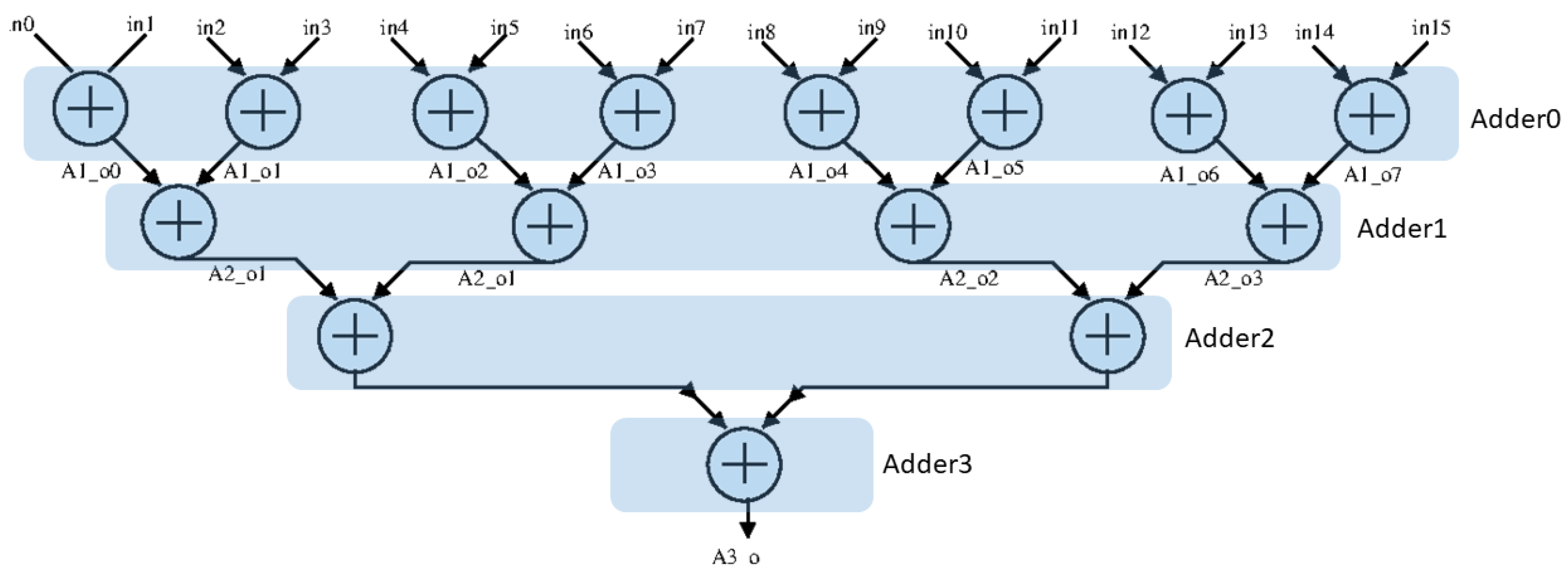
Figure 9b and Figure 10 illustrate the top adder module consisting of four adder blocks, and each adder block operated in the pipeline; hence, it could achieve the power reduction. The last adder block in the pipeline structure should be activated after the fourth clock cycle; thus, we could use the clock gating technique, and it was enabled by the previous adder block. We also used the same techniques for the other adders in the pipeline structure.
In the top module, all multipliers were enabled by the eninput and all executed in parallel; thus, these were gated by the single clock gating technique. Figure 11 shows the overall configuration of the CNN model that we applied as low-power techniques. Eighteen adder blocks operated in the pipeline with the clock gating technique applied to all blocks.
4. Experiment Results
In this article, we presented a method to achieve ultra-low power techniques at the RT-level, rather than a complex hardware design change for low power. Specifically, we focused on reducing power consumption through clock gating optimizations. Furthermore, we demonstrated our proposed technology through the CNN accelerator, which consumed the most power in the CNN architecture.
4.1. Testing Environment
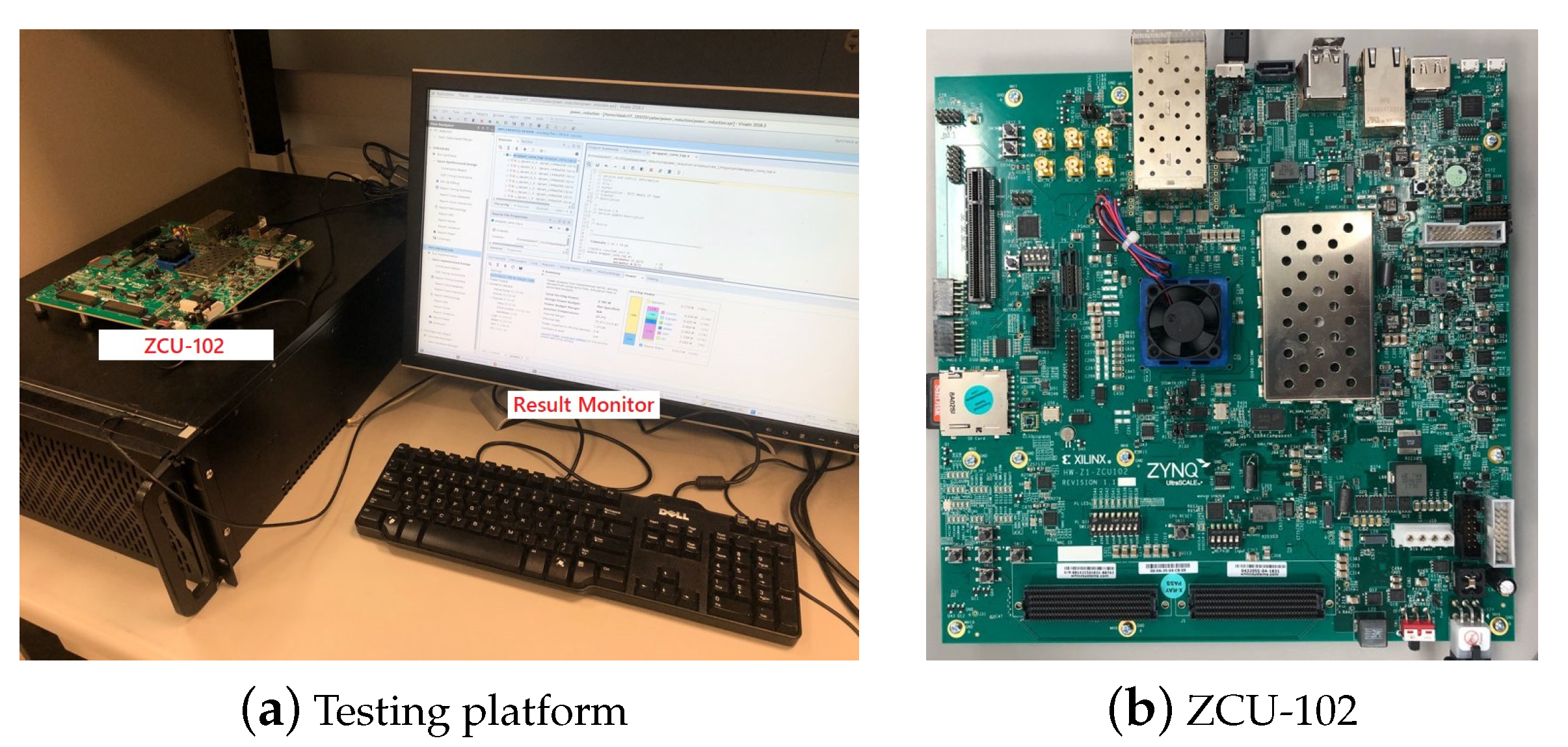
In order to verify our design of the CNN accelerator for the FPGA, we used the Xilinx Vivado for HLS design and the simulation in Figure 12.
According to all the parameters of the targeted board specification, the program provided an objective simulation result in different power dissipation types. Our targeted board was the Xilinx ZYNQ Ultrascale+ ZCU-102 FPGA SoC board with a quad-core ARM Cortex A-53, a dual-core Cortex processor R-5F, and an additional GPU based on Xilinx’s 16 nm FinFET+ programmable fabric. In addition, it contained 600 system logic cells, 32.1 Mb memory, and 2520 DSP slices. Additionally, for the ASIC verification, we used the FreePDK45 [31]: 45 nm Technology library and proceeded to logic synthesis using Synopsys Design Compiler. As a result, power analysis was performed by using the power results from synthesis, and the physical design was not performed for the power measurement.
4.2. FPGA Implementation Result
As we explored in the previous section, we applied three techniques, LECG, memory splitting, and multi-voltage scaling on the Xilinx Ultrascale+ ZCU102, FPGA SoC board. In Table 1 and Figure 13, using static power, the power savings amount was reduced by 4.22% compared to the original Verilog RTL code. In the dynamic power dissipation result, we were able to achieve 32.72% power reduction. The total power consumption was decreased by 28.01%.
As shown in Table 1, even though the power consumption seemed to be reduced by 1 watt, the more than 30% power reduction result showed that our suggested methods could be directly effective for the FPGA implementation of the CNN accelerator.
Table 2 shows the comparison result of the power consumption with state-of-the-art works. Since, we controlled unnecessary operation through the clock gating in dynamic operation mainly, our techniques appeared more effective in terms of dynamic power.
4.3. ASIC Implementation Result
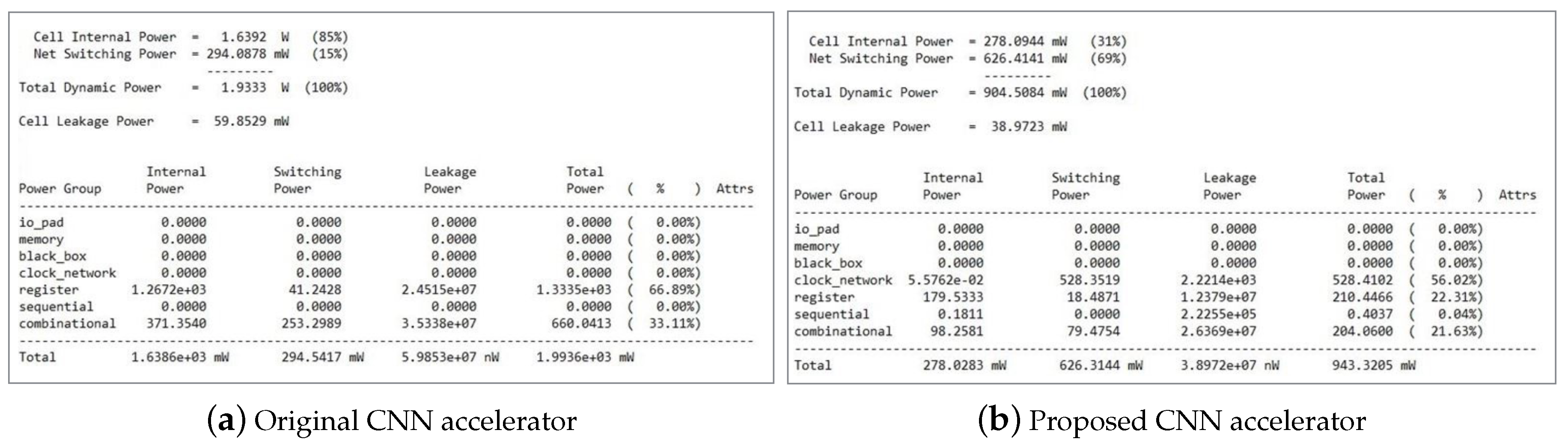
Along with the FPGA verification, we applied LECG and memory splitting techniques. In order to measure the power consumption in the ASIC design, we were not able to proceed with the physical design at this time due to the academic research lab limitations. Therefore, the multi-voltage scaling technique applied to FPGA was not applied. However, since we are currently working with the industry, we plan to proceed with the physical design with the industry in the near future. We used a 45 nm FreePDK library for the ASIC implementation and proceeded to logic synthesis through the Synopsys Design Compiler. We analyzed the power results verified through the logic synthesis, and the results are shown in Table 3. As described in Table 3 and Figure 14, we could reduce 34.9% of the power consumption in static power, and above all, we could reduce the power consumption in dynamic power by 53.21%. Overall, the total power consumption showed that our proposed CNN accelerator consumed 52.68% less power than previous approaches.
5. Conclusions
This article presented that we achieved low-power dissipation through the CNN-based accelerator implementation on the FPGA SoC board by using the representative effective techniques at the RT-level. Based on the result, we ascertained that applying the clock gating and the memory splitting techniques at the RT-level could reduce the power dissipation, not affecting the major functionality of the computational processing. In the FPGA hardware implementation, applying clock gating and memory splitting methods to the synthesized Verilog code, we were able to achieve up to a 32.72% power reduction of the dynamic power consumption on the convolution operation on the Xilinx ZYNQ Ultrascale+ ZCU-102. This entailed that the low-power techniques at the different levels of the design process enabled additional power dissipation reduction. Furthermore, in the ASIC implementation, the power dissipation was reduced by 52.68% using the same techniques applied to the FPGA implementation. This result represented that the low-power techniques on the different target device could achieve additional power dissipation reduction. Therefore, our experiment results facilitated greatly the optimization of the HLS design process when using a small size FPGA platform as the components of autonomous and electric vehicles. As for the future work, we will graft those techniques into the CNN accelerator design for ASIC fabrication so that we can achieve the low-power design solution for improving the power efficiency of autonomous vehicles.
Author Contributions
Conceptualization, Data curation, Formal analysis, Investigation, Methodology, Validation, Y.K., H.K., N.Y. and S.L.; Writing—original draft, Writing—review and editing, Y.K., H.K., N.Y. and K.K.C.; Supervision, Funding acquisition, Project administration, K.K.C. All authors read and agreed to the published version of the manuscript.
Funding
This work is supported by the Industrial Core Technology Development Program of MOTIE/KEIT, KOREA. (#10083639, Development of Camera-based Real-time Artificial Intelligence System for Detecting Driving Environment & Recognizing Objects on Road Simultaneously).
Acknowledgments
We thank our colleagues from KETIand KEITwho provided insight and expertise that greatly assisted the research and greatly improved the manuscript.
Conflicts of Interest
The authors declare no conflicts of interest.
References
- Nishani, E.; Çiço, B. Computer vision approaches based on deep learning and neural networks: Deep neural networks for video analysis of human pose estimation. In Proceedings of the 2017 6th Mediterranean Conference on Embedded Computing (MECO), Bar, Montenegro, 11–15 June 2017; pp. 1–4. [Google Scholar] [CrossRef]
- Zhao, Y.; Zhao, J.; Zhao, C.; Xiong, W.; Li, Q.; Yang, J. Robust Real-Time Object Detection Based on Deep Learning for Very High Resolution Remote Sensing Images. In Proceedings of the IGARSS 2019—2019 IEEE International Geoscience and Remote Sensing Symposium, Yokohama, Japan, 28 July–2 August 2019; pp. 1314–1317. [Google Scholar] [CrossRef]
- Zhang, Y.; Ming, Y.; Zhang, R. Object Detection and Tracking based on Recurrent Neural Networks. In Proceedings of the 2018 14th IEEE International Conference on Signal Processing (ICSP), Beijing, China, 12–16 August 2018; pp. 338–343. [Google Scholar] [CrossRef]
- Liu, W.; Anguelov, D.; Erhan, D.; Szegedy, C.; Reed, S.E.; Fu, C.; Berg, A.C. SSD: Single Shot MultiBox Detector. arXiv 2015, arXiv:1512.02325. [Google Scholar]
- Ren, S.; He, K.; Girshick, R.B.; Sun, J. Faster R-CNN: Towards Real-Time Object Detection with Region Proposal Networks. arXiv 2015, arXiv:1506.01497. [Google Scholar] [CrossRef] [PubMed] [Green Version]
- Redmon, J.; Farhadi, A. YOLO9000: Better, Faster, Stronger. arXiv 2016, arXiv:1612.08242. [Google Scholar]
- Pan, S.; Shi, L.; Guo, S.; Guo, P.; He, Y.; Xiao, R. A low-power SoC-based moving target detection system for amphibious spherical robots. In Proceedings of the 2015 IEEE International Conference on Mechatronics and Automation (ICMA), Beijing, China, 2–5 August 2015; pp. 1116–1121. [Google Scholar] [CrossRef]
- Liu, W.; Chen, H.; Ma, L. Moving object detection and tracking based on ZYNQ FPGA and ARM SOC. In Proceedings of the IET International Radar Conference 2015, Hangzhou, China, 14–16 October 2015; pp. 1–4. [Google Scholar] [CrossRef]
- Padmanabha, M.; Schott, C.; Rößler, M.; Kriesten, D.; Heinkel, U. ZYNQ flexible platform for object recognition tracking. In Proceedings of the 2016 13th Workshop on Positioning, Navigation and Communications (WPNC), Bremen, Germany, 19–20 October 2016; pp. 1–6. [Google Scholar] [CrossRef]
- Desmouliers, C.; Aslan, S.; Oruklu, E.; Saniie, J.; Vallina, F.M. HW/SW co-design platform for image and video processing applications on Virtex-5 FPGA using PICO. In Proceedings of the 2010 IEEE International Conference on Electro/Information Technology, Normal, IL, USA, 20–22 May 2010; pp. 1–6. [Google Scholar] [CrossRef]
- Canziani, A.; Paszke, A.; Culurciello, E. An Analysis of Deep Neural Network Models for Practical Applications. arXiv 2016, arXiv:1605.07678. [Google Scholar]
- Nakahara, H.; Yonekawa, H.; Fujii, T.; Sato, S. A Lightweight YOLOv2: A Binarized CNN with A Parallel Support Vector Regression for an FPGA. In Proceedings of the 2018 ACM/SIGDA International Symposium on Field-Programmable Gate Arrays, Monterey, CA, USA, 25–27 February 2018; pp. 31–40. [Google Scholar] [CrossRef]
- Hardware Acceleration of Deep Neural Networks: GPU, FPGA, ASIC, TPU, VPU, IPU, DPU, NPU, RPU, NNP and Other Letters. Available online: https://itnesweb.com/article/hardware-acceleration-of-deep-neural-networks-gpu-fpga-asic-tpu-vpu-ipu-dpu-npu-rpu-nnp-and-other-letters (accessed on 12 March 2020).
- Pedram, M.; Abdollahi, A. Low-power RT-level synthesis techniques: A tutorial. IEE Proc. Comput. Digit. Tech. 2005, 152, 333–343. [Google Scholar] [CrossRef] [Green Version]
- Zhang, C.; Li, P.; Sun, G.; Guan, Y.; Xiao, B.; Cong, J. Optimizing FP GA-based Accelerator Design for Deep Convolutional Neural Networks. In Proceedings of the 2015 ACM/SIGDA International Symposium on Field-Programmable Gate Arrays, Monterey, CA, USA, 22–24 February 2015; pp. 161–170. [Google Scholar] [CrossRef]
- Alwani, M.; Chen, H.; Ferdman, M.; Milder, P. Fused-layer CNN accelerators. In Proceedings of the 2016 49th Annual IEEE/ACM International Symposium on Microarchitecture (MICRO), Taipei, Taiwan, 15–19 October 2016; pp. 1–12. [Google Scholar] [CrossRef]
- Sun, F.; Wang, C.; Gong, L.; Xu, C.; Zhang, Y.; Lu, Y.; Li, X.; Zhou, X. A High-Performance Accelerator for Large-Scale Convolutional Neural Networks. In Proceedings of the 2017 IEEE International Symposium on Parallel and Distributed Processing with Applications and 2017 IEEE International Conference on Ubiquitous Computing and Communications (ISPA/IUCC), Guangzhou, China, 12–15 December 2017; pp. 622–629. [Google Scholar] [CrossRef]
- Shen, Y.; Ferdman, M.; Milder, P. Maximizing CNN Accelerator Efficiency Through Resource Partitioning. arXiv 2016, arXiv:1607.00064. [Google Scholar] [CrossRef] [Green Version]
- Li, L.; Choi, K.; Park, S.; Chung, M. Selective clock gating by using wasting toggle rate. In Proceedings of the 2009 IEEE International Conference on Electro/Information Technology, Windsor, ON, Canada, 7–9 June 2009; pp. 399–404. [Google Scholar] [CrossRef]
- Wang, W.; Tsao, Y.-C.; Choi, K.; Park, S.M.; Chung, M.-K. Pipeline power reduction through single comparator-based clock gating. In Proceedings of the 2009 International SoC Design Conference (ISOCC), Busan, Korea, 22–24 November 2009; pp. 480–483. [Google Scholar] [CrossRef]
- Zhang, Y.; Tong, Q.; Li, L.; Wang, W.; Choi, K.; Jang, J.; Jung, H.; Ahn, S. Automatic Register Transfer level CAD tool design for advanced clock gating and low power schemes. In Proceedings of the 2012 International SoC Design Conference (ISOCC), Jeju Island, Korea, 4–7 November 2012; pp. 21–24. [Google Scholar] [CrossRef]
- Kim, H.; Choi, K. The Implementation of a Power Efficient BCNN-Based Object Detection Acceleration on a Xilinx FPGA-SoC. In Proceedings of the 2019 International Conference on Internet of Things (iThings) and IEEE Green Computing and Communications (GreenCom) and IEEE Cyber, Physical and Social Computing (CPSCom) and IEEE Smart Data (SmartData), Atlanta, GA, USA, 14–17 July 2019; pp. 240–243. [Google Scholar] [CrossRef]
- Ma, Y.; Cao, Y.; Vrudhula, S.; Seo, J. Optimizing the Convolution Operation to Accelerate Deep Neural Networks on FPGA. IEEE Trans. Very Large Scale Integr. (VLSI) Syst. 2018, 26, 1354–1367. [Google Scholar] [CrossRef]
- Nguyen, D.T.; Nguyen, T.N.; Kim, H.; Lee, H. A High-Throughput and Power-Efficient FPGA Implementation of YOLO CNN for Object Detection. IEEE Trans. Very Large Scale Integr. (VLSI) Syst. 2019, 27, 1861–1873. [Google Scholar] [CrossRef]
- Fraser, N.J.; Umuroglu, Y.; Gambardella, G.; Blott, M.; Leong, P.H.W.; Jahre, M.; Vissers, K.A. Scaling Binarized Neural Networks on Reconfigurable Logic. arXiv 2017, arXiv:1701.03400. [Google Scholar]
- Lin, D.D.; Talathi, S.S.; Annapureddy, V.S. Fixed Point Quantization of Deep Convolutional Networks. arXiv 2015, arXiv:1511.06393. [Google Scholar]
- Ioffe, S.; Szegedy, C. Batch Normalization: Accelerating Deep Network Training by Reducing Internal Covariate Shift. arXiv 2015, arXiv:1502.03167. [Google Scholar]
- Aydonat, U.; O’Connell, S.; Capalija, D.; Ling, A.C.; Chiu, G.R. An OpenCL(TM) Deep Learning Accelerator on Arria 10. arXiv 2017, arXiv:1701.03534. [Google Scholar]
- Zhao, Y.; Zhang, X.; Fang, X.; Li, L.; Li, X.; Guo, Z.; Liu, X. A Deep Residual Networks Accelerator on FPGA. In Proceedings of the 2019 Eleventh International Conference on Advanced Computational Intelligence (ICACI), Guilin, China, 7–9 June 2019; pp. 13–17. [Google Scholar] [CrossRef]
- Kim, H.; Choi, K. Low Power FPGA-SoC Design Techniques for CNN-based Object Detection Accelerator. In Proceedings of the 2019 IEEE Annual Ubiquitous Computing, Electronics & Mobile Communication Conference, New York City, NY, USA, 10–12 October 2019. [Google Scholar]
- FreePDK45:Contents. Available online: https://www.eda.ncsu.edu/wiki/FreePDK45:Contents (accessed on 12 March 2020).
- Zhijie, Y.; Lei, W.; Li, L.; Shiming, L.; Shasha, G.; Shuquan, W. Bactran: A Hardware Batch Normalization Implementation for CNN Training Engine. IEEE Embed. Syst. Lett. 2020. [Google Scholar] [CrossRef]
- Piyasena, D.; Wickramasinghe, R.; Paul, D.; Lam, S.; Wu, M. Reducing Dynamic Power in Streaming CNN Hardware Accelerators by Exploiting Computational Redundancies. In Proceedings of the 2019 29th International Conference on Field Programmable Logic and Applications (FPL), Barcelona, Spain, 8–12 September 2019; pp. 354–359. [Google Scholar] [CrossRef]
Figure 1.
FPGA-based CNN accelerator architecture. PE, processing element.

Figure 2.
CNN computational process overview.

Figure 3.
Conventional register versus register with local explicit clock Enable (LECE).

Figure 4.
Local explicit clock gating (LECG).

Figure 5.
(a) Bus-specific clock gating (BSCG); (b) enhanced clock gating (ECG).

Figure 6.
Applied memory split technique to the CNN.

Figure 7.
Proposed CNN accelerator architecture.

Figure 8.
Applied local explicit clock gating (LECG) to the multiplier for CNN.

Figure 9.
Applied local explicit clock gating (LECG) technique.

Figure 10.
Four stage pipeline structure of the adder block.

Figure 11.
Overall CNN configuration with local explicit clock gating (LECG) technique.

Figure 12.
Configuration of the testing environment.

Figure 13.
Power consumption comparison of the CNN accelerator on FPGA.

Figure 14.
Power consumption comparison of the CNN accelerator on ASIC.


Table 1.
Power consumption comparison of the CNN accelerator on FPGA.
| Original | Proposed | Power Reduction | |
|---|---|---|---|
| Static Power | 0.639 W | 0.612 W | 4.22% |
| Dynamic Power | 3.230 W | 2.173 W | 32.72% |
| Total Power | 3.869 W | 2.785 W | 28.01% |
Table 2.
Comparison of the power consumption with state-of-the-art works.
| S.No. | Static Power (W) | Dynamic Power (W) | Total Power (W) | Reference |
|---|---|---|---|---|
| 1 | 2.827 | 6.123 | 8.950 | [32] |
| 2 | – | 2.205 | – | [33] |
| 3 | 0.612 | 2.173 | 2.785 | This work |
Table 3.
Power consumption comparison of the CNN accelerator on ASIC.
| Original | Proposed | Power Reduction | |
|---|---|---|---|
| Static Power | 0.0598 W | 0.0389 W | 34.9 % |
| Dynamic Power | 1.9333 W | 0.9045 W | 53.21 % |
| Total Power | 1.9936 W | 0.9432 W | 52.68 % |
© 2020 by the authors. Licensee MDPI, Basel, Switzerland. This article is an open access article distributed under the terms and conditions of the Creative Commons Attribution (CC BY) license (http://creativecommons.org/licenses/by/4.0/).
Share and Cite
MDPI and ACS Style
Kim, Y.; Kim, H.; Yadav, N.; Li, S.; Choi, K.K. Low-Power RTL Code Generation for Advanced CNN Algorithms toward Object Detection in Autonomous Vehicles. Electronics 2020, 9, 478. https://doi.org/10.3390/electronics9030478
AMA Style
Kim Y, Kim H, Yadav N, Li S, Choi KK. Low-Power RTL Code Generation for Advanced CNN Algorithms toward Object Detection in Autonomous Vehicles. Electronics. 2020; 9(3):478. https://doi.org/10.3390/electronics9030478
Chicago/Turabian StyleKim, Youngbae, Heekyung Kim, Nandakishor Yadav, Shuai Li, and Kyuwon Ken Choi. 2020. "Low-Power RTL Code Generation for Advanced CNN Algorithms toward Object Detection in Autonomous Vehicles" Electronics 9, no. 3: 478. https://doi.org/10.3390/electronics9030478
Note that from the first issue of 2016, this journal uses article numbers instead of page numbers. See further details here.