Energy-Efficient Ternary Multipliers Using CNT Transistors
by
 , and
, and
Sepehr Tabrizchi
1 ,
,
Atiyeh Panahi
1,
Fazel Sharifi
2,
Hamid Mahmoodi
3 and
Abdel-Hameed A. Badawy
4,* 1
Faculty of Computer Science and Engineering, Shahid Beheshti University G. C., Tehran 1983963113, Iran
2
Department of Electrical and Computer Engineering, Graduate University of Advanced Technology, Kerman 7631133131, Iran
3
Department of Electrical and Computer Engineering, San Francisco State University, San Francisco, CA 94132, USA
4
Klipsch School of Electrical and Computer Engineering, New Mexico State University, Las Cruces, NM 88003, USA
*
Author to whom correspondence should be addressed.
Electronics 2020, 9(4), 643; https://doi.org/10.3390/electronics9040643
Submission received: 5 March 2020
/
Revised: 26 March 2020
/
Accepted: 31 March 2020
/
Published: 14 April 2020
(This article belongs to the Section Microelectronics)
Abstract
:In recent decades, power consumption has become an essential factor in attracting the attention of integrated circuit (IC) designers. Multiple-valued logic (MVL) and approximate computing are some techniques that could be applied to integrated circuits to make power-efficient systems. By utilizing MVL-based circuits instead of binary logic, the information conveyed by digital signals increases, and this reduces the required interconnections and power consumption. On the other hand, approximate computing is a class of arithmetic computing used in systems where the accuracy of the computation can be traded-off for lower energy consumption. In this paper, we propose novel designs for exact and inexact ternary multipliers based on carbon-nanotube field-effect transistors (CNFETs). The unique characteristics of CNFETs make them a desirable alternative to MOSFETs. The simulations are conducted using Synopsys HSPICE. The proposed design is compared against existing ternary multipliers. The results show that the proposed exact multiplier reduces the energy consumption by up to 6 times, while the best inexact design improves energy efficiency by up to 35 time compared to the latest state-of-the-art methods. Using the imprecise multipliers for image processing provides evidence that these proposed designs are a low-power system with an acceptable error.
1. Introduction
The rapid evolution of the semiconductor industry has increased the number of components and complexity per unit area of a chip. Moore’s law has set a growth roadmap for the IC industry to double the number of transistors per unit area in every new generation of devices and technology. Consequently, the feature size of transistors shrunk by 0.7X every two years following Moore’s law [1]. The natural consequences of a decrease in the size of MOS transistors lead to challenges such as the increase of leakage current, quantum physical effects, and major complications as the results of thermal fluctuations, to name a few [1]. Researchers have been exploring emerging material and devices to replace classic MOS transistors and silicon-based chips as the beyond Moore’s law alternatives. Resonant tunneling diodes (RTD), single-electron transistors (SET), quantum-dot cellular automata (QCA), and finally, carbon nanotube field-effect transistors (CNFET) are the most outstanding alternatives for MOSFET [2,3,4,5].
Among all the emerging nano-devices, carbon nanotubes are the most promising candidates for channel material in the future generation of transistors because of their ballistic transportation and their thin bodies and for other reasons [6]. Carbon nanotube field-effect transistors operate faster, with less energy consumption compared to their silicon counterparts [7]. There are many similarities in the inherent characteristics of CNFETs and MOSFETs. Such similarities make CNFETs the appropriate replacement for MOSFET-like circuits with just a minor change in the MOSFET platform [8]. Also, CNFETs benefit from their adjustable threshold voltage, which is as easy as setting the diameter of the nanotube. In other words, the threshold voltage of CNFETs only depends on the diameter of the under-gate nanotubes. This unique characteristic of CNFETs makes them appropriate for designing MVL circuits [9].
MVL designs use more than two logic levels for representing their values. Compared to binary logic, each digit in MVL represents more data: therefore, the bandwidth and the number of lines for data transmission are less. On the other hand, for conceptual and implementation issues, choosing the optimal radix is of great importance [10]. For radix selection, we need a performance measurement metric. The product value of the radix by the required number of digits, which expresses a fixed range of numbers, is the performance measurement metric of choice.
Regarding the metric above, -based ( = 2.718) operations are the optimum case. Ternary logic is superior to binary logic if we use the above metric since three is the closest integer to [11]. Ternary logic provides the most efficiency with its lower energy consumption as a result of the reduction in the number of interconnection wires and the cost of data carriage [11].
Energy consumption is a primary concern in current and future systems [12]. Using MVL and low-power technologies such as CNFETs can reduce the power dissipation of arithmetic and logic circuits. Another low power technique that researchers have explored is approximate or inexact computing [13]. In approximate arithmetic circuits, for some input combinations, the output of the design is inexact. Such designs will reach minimum power consumption by using less hardware. Hence, the designs will have a lower area while sacrificing computation accuracy but meeting an acceptable accuracy [13]. Approximate computing has its applications in digital signal processing, including voice and image processing [13]. In these applications, exact computing is not as important as in other arithmetic applications. Humans cannot distinguish minute imperfection in audio and video [13]. An approximation can be applied at different levels of design abstraction from algorithms to circuit design. Imprecise circuits such as approximate logical gates, adders, and multipliers could be useful in media processing without significant degradation in the output quality. Multipliers are one of the basic blocks used in different DSP applications, such as image filtering or image multiplication [13]. Therefore, an inexact multiplier with a reasonable error can improve energy efficiency in signal processing applications significantly.
In this paper, we propose a novel CNFET-based ternary one-trit multiplier. This exact design has less power and energy consumption compared to the other state-of-the-art designs. To reap the benefits of approximate computing, we propose to convert exact designs into inexact designs with a minor change in the original exact methodology. In this work, we have applied approximate designs in image processing applications, and the results show a balanced design trade-off between the accuracy and the energy consumption of the proposed designs.
The rest of the paper is organized as follows: The next section describes in detail the structure, merits, and demerits of CNFETs. Section 3 illustrates the detailed structure of the proposed designs. Section 4 contains the simulation results of the proposed exact and inexact designs and compares them to existing methods. Section 5 presents the results of utilizing the proposed methods in image processing applications, and finally, Section 6 concludes the paper.
2. Carbon Nanotube Field-Effect Transistor (CNFET)
A carbon nanotube (CNT) is a sheet of graphene rolled up like a tube with a diameter in the order of nanometers [14]. These graphene tubes are used as the gate channels in CNFETs. A CNT can be a single-walled CNT (SWCNT), which is composed of a single tube, or it can be a multi-walled CNT (MWCNT), which has several tubes that have been rolled up inside each other [15]. Some favorable characteristics of single-walled CNFETs include lower short channel effects in short channel lengths, higher gain, larger ION/IOFF ratio, reduced power consumption as a result of ballistic transport in a transistor body with one-dimensional structure. These advantages are why many researchers feel that carbon nanotubes are a suitable candidate for future transistors [16,17].
Carbon nanotube transistors are grouped into three different types, which have been named Schottky-Barrier (SB), partially gated (PG), and doped S/D CNFET. The first group has robust ambipolar characteristics and a small ION/IOFF ratio. In this type of CNFETs, gate bias determines the transistor functionality. Hence, it is not suitable for conventional CMOS logic families. The second group is uniformly doped and works in depletion mode. Doped S/D transistors, the third group, work in enhancement or depletion mode. They have a unipolar characteristic and reduced OFF leakage current and are suitable for MOSFET-like circuits [18].
The atomic structure of CNFETs is determined by the chiral vector . To be more specific, and indices determine the chirality, and chirality affects conductance. For instance, a nanotube is metallic if the difference of these vector indices is divisible by three; otherwise, the nanotube is a semiconductor. As described in [19], indices determine the perimeter vector, as defined in Equation (1).
In this case, and are the basis vectors of graphene lattice. They separated by an inter-angle of 60 with (. The magnitude value of the vector is calculated as in Equation (2). Equation (3) calculate the diameter of the nanotube. (3) [19].
In the above equations, is the basis vector of graphene lattice, and and are chiral vector indices. The following Equation (4) determines the threshold voltage of CNFETs [20].
where is the carbon-to-carbon atom distance, . is the carbon . band energy in the tight bonding model, is the unit electron charge, and is the diameter of CNTs, as calculated in Equation (3). By considering (1) through (4), we can conclude that the threshold voltage of CNFETs depends on the diameter of the under-gate tubes; and, consequently, by changing the chiral vector indices, nanotube diameter and the threshold voltage are set quickly. This important unique characteristic of CNFETs makes them suitable for use in MVL logic circuits.
Due to the properties mentioned above for carbon nanotube-based transistors, we utilize single-walled S/D CNFETs for designing ternary exact and inexact multipliers.
3. Proposed Work
This section describes the proposed ternary multipliers in detail. It is essential to mention that in ternary logic, the output is equal to “0”, “1”, or “2” logic levels with equivalent voltages of “0”, “”, and “”. As mentioned previously, we propose an exact multiplier which has two ternary input digits and a ternary product and carry digits as outputs. Table 1 shows the truth table. Then, we relaxed the exact output’s result of the cell for an input combination to reach better performance in specific applications like DSP. The approximate designs are different from the exact ones because of the elimination of some parts of the exact circuit.
3.1. The Proposed Exact Design
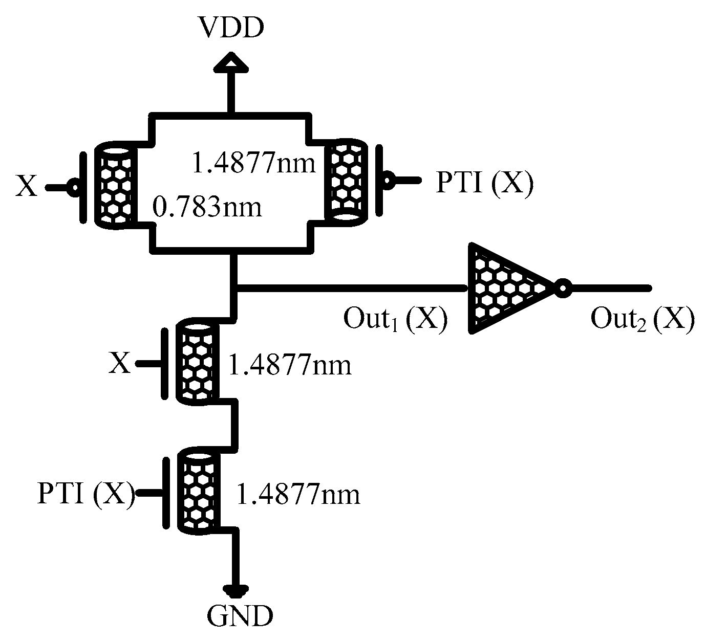
In this section, the proposed exact design of the ternary one-trit multiplier is described. First of all, it is essential to mention that in the schematic design of all the proposed methods, is the output of the circuit, as shown in Figure 1. This circuit gets a ternary digit of as its input and produces and as binary outputs. is the negated of the that is utilized in the proposed methods. The truth table of these two outputs is illustrated in Table 2. Also, in the schematic of the circuits, the NTI and PTI are negative ternary inverter and positive ternary inverter, respectively, their functions are detailed in Table 2 [8].
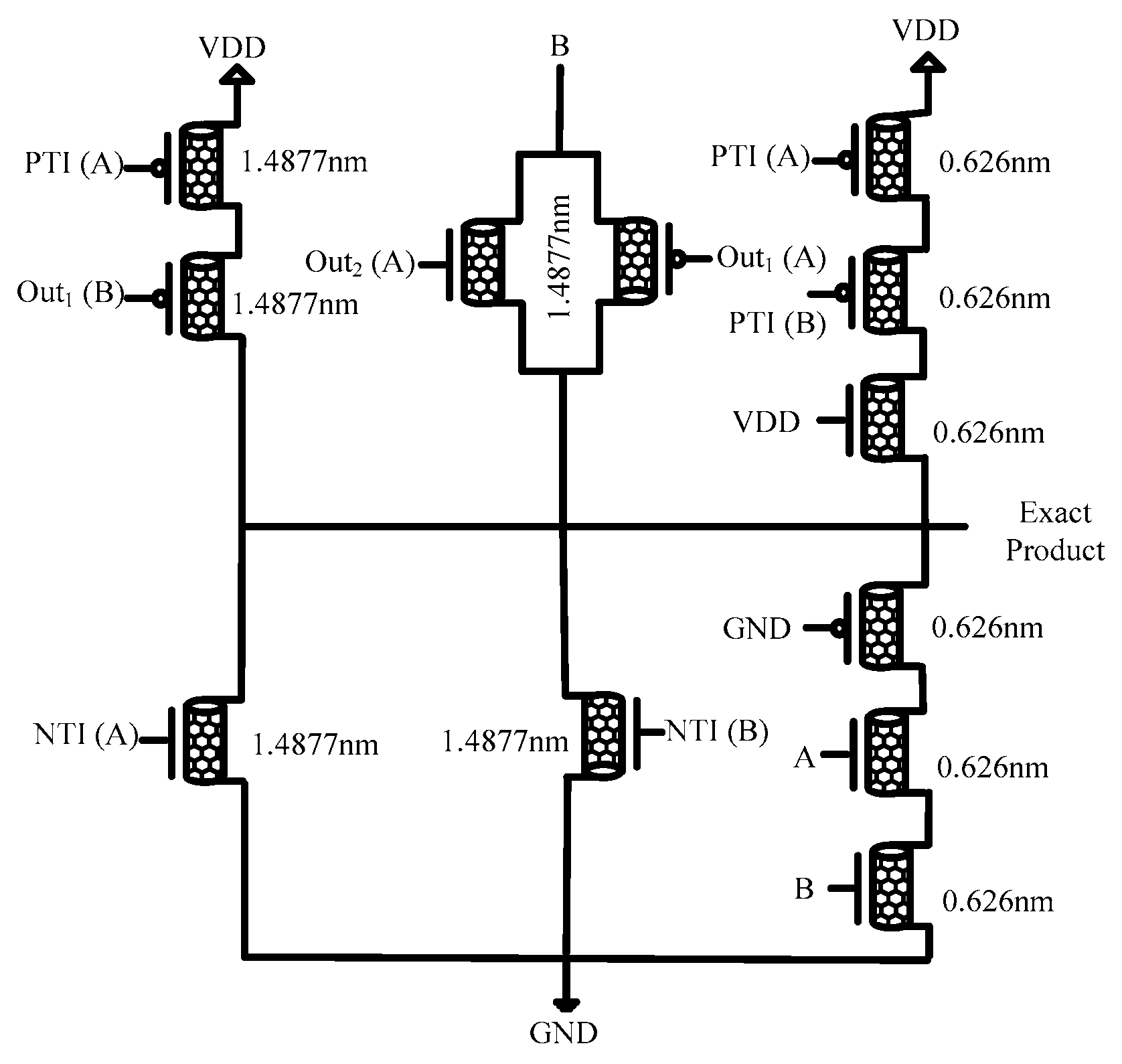
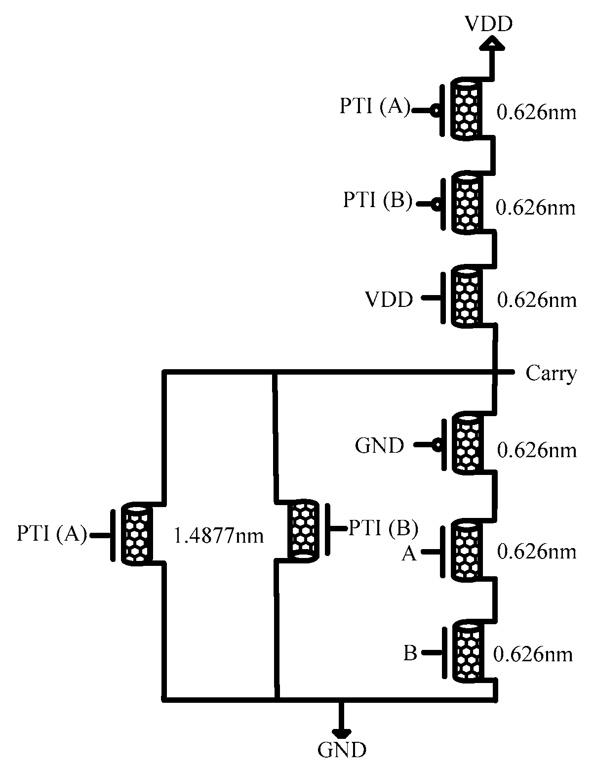
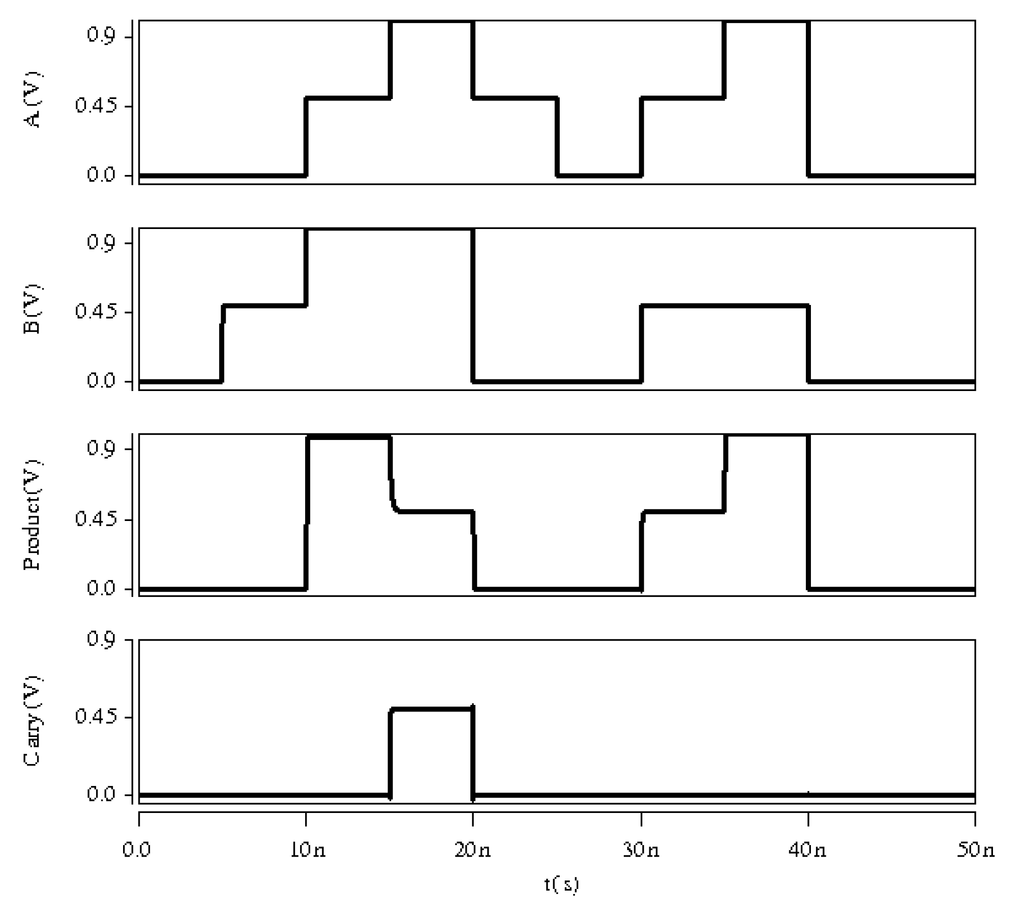
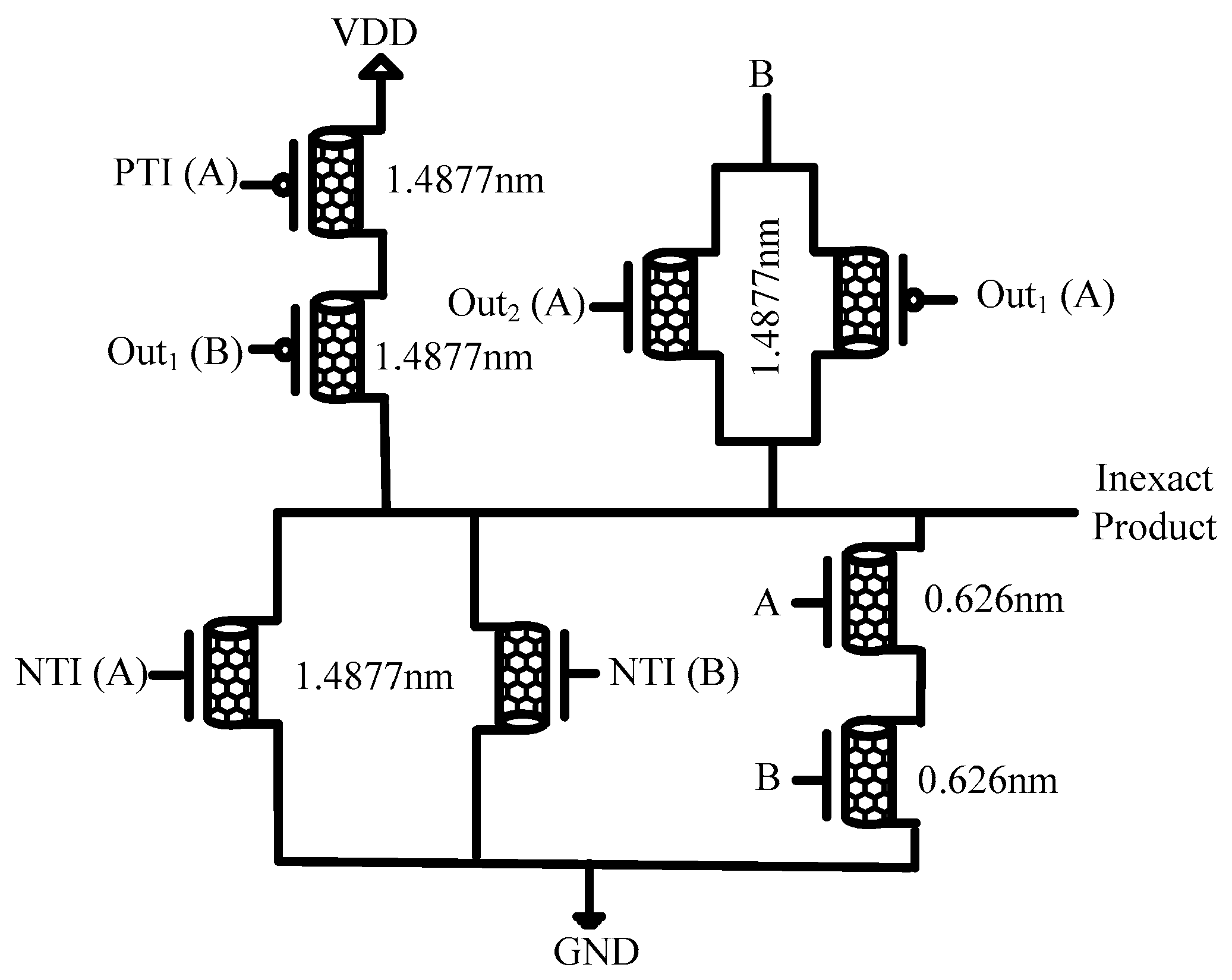
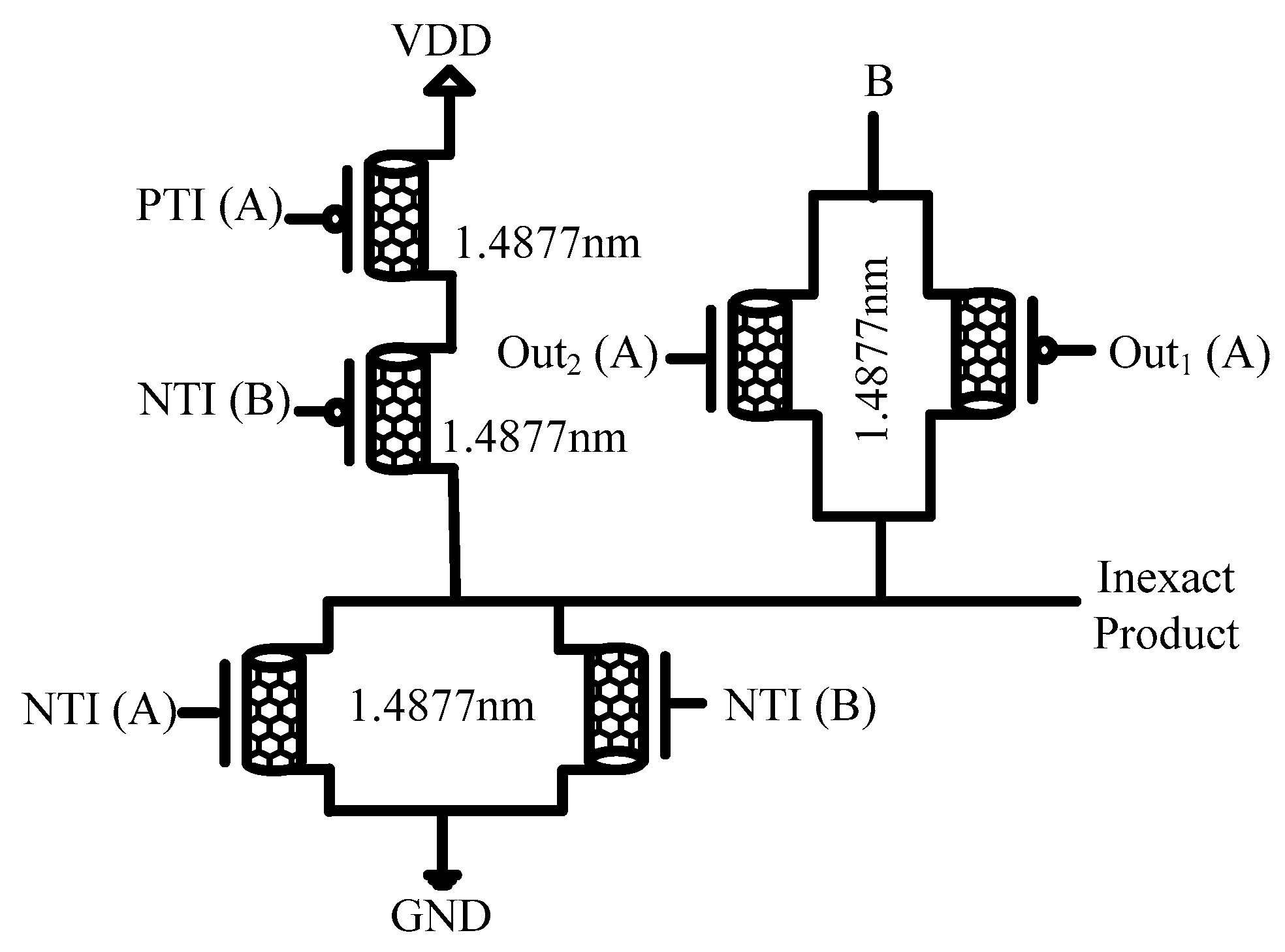
The schematic design of the exact product digit is shown in Figure 2. We can conclude from Figure 2, and the truth table of a one-trit multiplier shown in Table 1, for the first three input combinations, only the leftmost NFET of the pull-down network will be ON since NTI (A) would be logically equal to “2”. For the input conditions that the first input is equivalent to “1”, the middle transmission gate of the pull-up network turns on, and the second input reaches to the output node. If the input digits would be equal to “20” or “21”, the middle NFET of pull-down network and the two leftmost PFETs of the pull-up network will be activated, respectively. For the last input combination wherein both of the inputs are equal to “2”, the rightmost transistors turn on. In other words, for this condition, the product digit should be equal to “1”; hence, both of the pull-up and pull-down networks are active, and by a resistive division, the output becomes logically equal to “1”. The proposed design for the carry out digit has been illustrated in Figure 3 and its output is “0” for all input conditions except for the last input combination of Table 1. In this situation, the pull-up network and the rightmost NFET transistors of the pull-down network go ON, and the result would be equal to “” at the carry output node. The method for voltage dividing to produce “” at the output is more detailed in [21]. The transient responses of the proposed exact multiplier are shown in Figure 4, which confirms its correct operation.
3.2. The Proposed Inexact Designs
In this section, the proposed inexact designs are discussed further. Generally, these inexact designs relax the product or carry output digit for only the last inputs combination of Table 1, which is encircled. The reason for allowing this input combination to be imprecise is that this is the only combination in which the value of its output is equal to “1,” while none of the inputs are “1”. Thus, the design of outputs will be more costly since the outputs can not be reached by using of any inputs directly. This relaxation occurs by removing some parts of the exact design and consequently having an inexact result at the output.
3.2.1. First Inexact Design
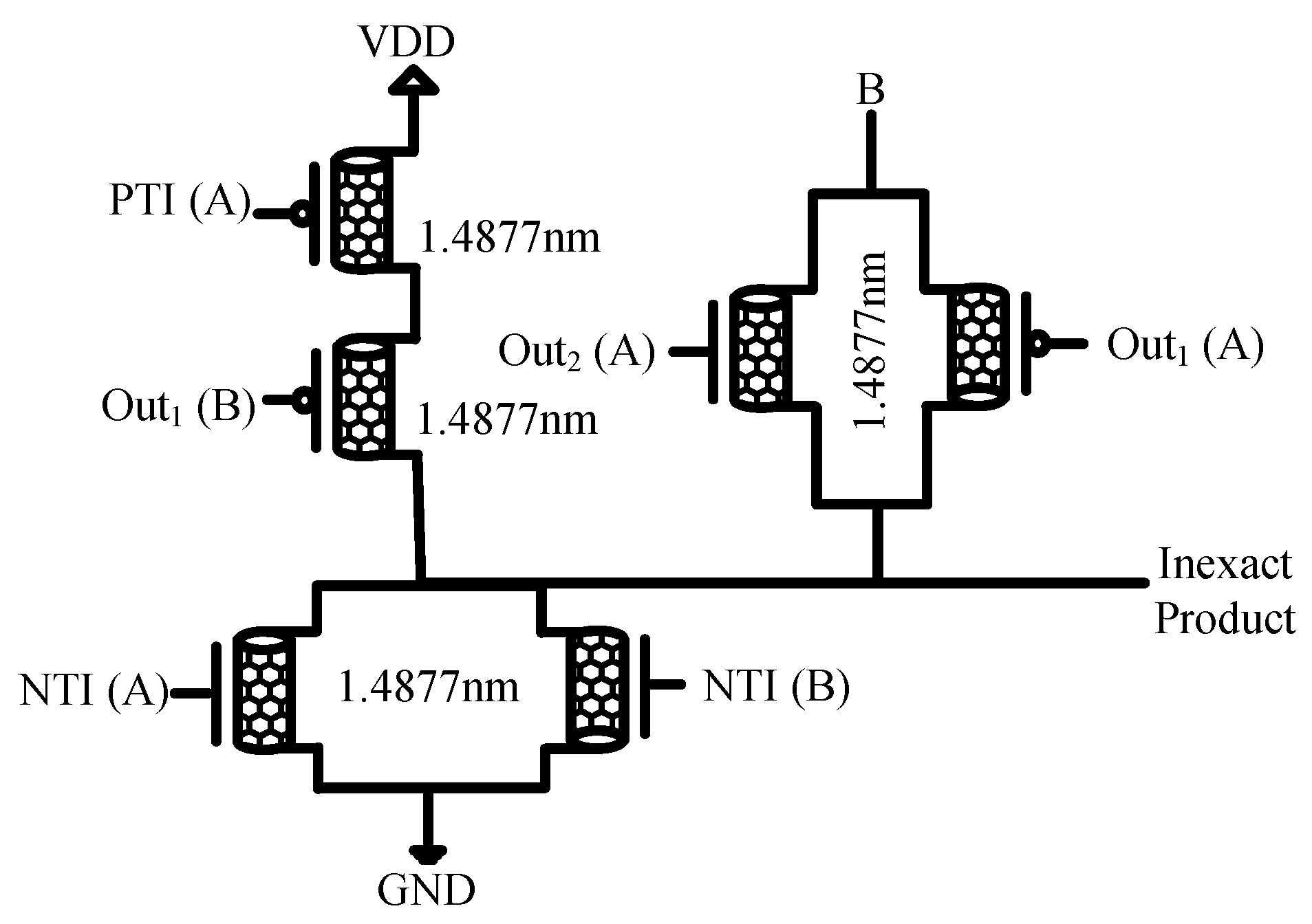
In this design, the product digit of the ternary multiplier would equal “0” for the last input condition of Table 1. Also, in this design, the carry output digit is equal to “0” for all input combinations. In other words, we have the output of “00” for the input combination of “22”. Figure 5 shows the schematic at the transistor level of the first design method, which is a modified version of the exact design we discussed previously.
3.2.2. Second Inexact Design
As we know, the product digit for the input digits of “22” is equal to “1” in the exact methods. Nevertheless, just like the first inexact method, the last part of the exact design is eliminated, which causes the product digit to be logically equal to “2” for this input combination. The schematic design of the second inexact method has been shown in Figure 6. The second method also considers the inexact carry output. In this design, the carry output digit would be equal to zero for all of the inputs. Hence, the circuit which generates the carry output is eliminated, and the carry output node is connected to the ground voltage to be equal to “0”.
3.2.3. Third Inexact Design
The main idea of designing this circuit is to have an exact carry output digit to have a more precise design. The product digit of this method is the same as the first inexact design. Therefore, we have “1” and “0” at the carry and product outputs respectively for the “22” input pattern.
3.2.4. Fourth Inexact Design
The significant difference between the second and fourth designs is that the output carry is exact in this design. But its product digit would be equal to “2” for the “22” input combination, just like the second method.
3.2.5. Fifth Inexact Design
Finally, this design keeps the previous value of the product digit for the “22” input pattern. Figure 7 represents the schematic design of this circuit. If the two input trits were logically equal to “2”, none of the paths will be active, and the output capacitor holds the previous product value. This design is exact for some input chains and inexact for some others. If the previous value of the product digit is equal to “1” and both of the next inputs would be equal to “2”, the product digit is “1”, and hence, it would be an exact result. The probability of an exact product result is more than the other proposed inexact designs. It should be mentioned that the carry output is exact in this design. It seems that this is a sufficient accuracy for most DSP applications. This will be further discussed in the next sections of this paper. Table 3 shows the truth table of all proposed inexact ternary multipliers.
4. Simulation Results
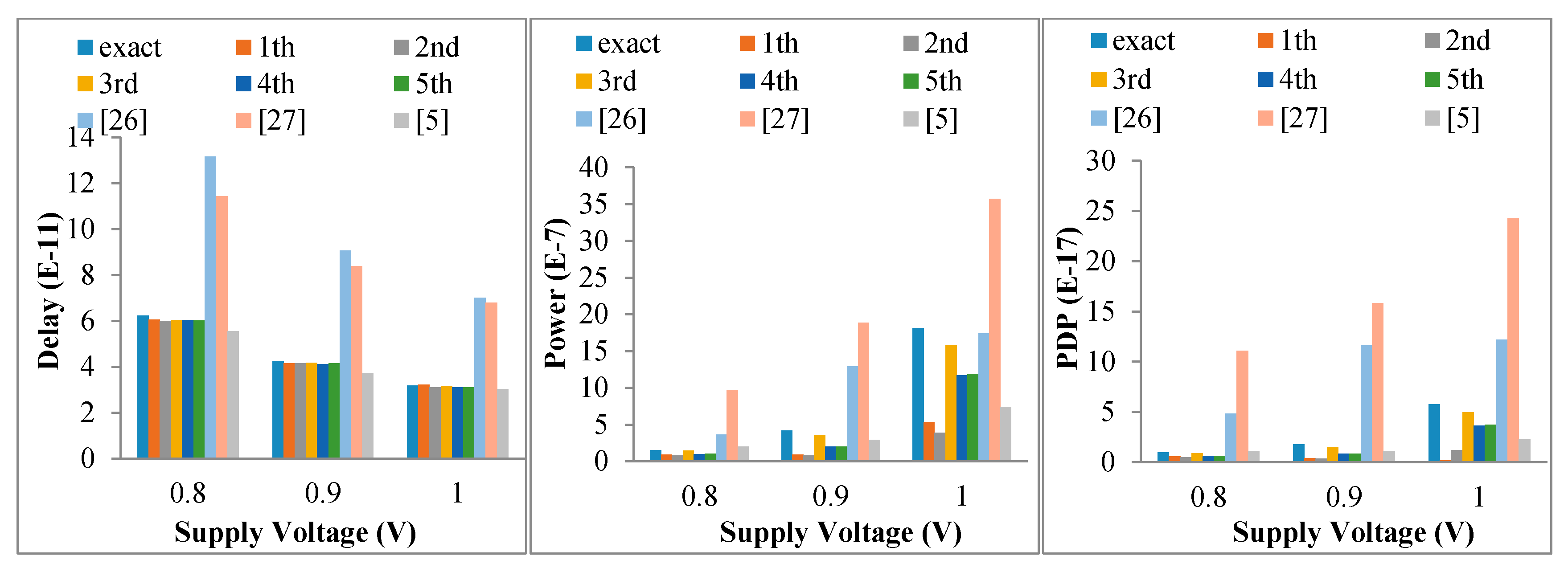
This section presents the simulation results of all the proposed designs in detail. Simulations are conducted in Synopsys HSPICE with the compact SPICE model for CNFET devices presented in [22,23,24]. Table 4 shows some critical parameters of this model. For fairness, for all designs in our simulations, the number of nanotubes under the gates for any transistor is fixed to five. The delay, power, and energy consumption of the proposed designs are compared with the previous exact designs in Table 5 for 200 MHz operational frequency and a 2fF load capacitor at the output nodes. To compare the area of the proposed designs with existing designs in the literature, the number of transistors and the total width of transistors for each design are compared as metrics of the area [25]. The proposed exact and inexact designs reduce the delay, power, and energy consumption compared to the previous methods [26,27]. But our designs have higher delay compared to the design of [5]. Design of [5] also has lower power consumtion than the proposed exact and third inexact designs. It should be mentioned that the ternary multiplier presented in [5] uses two supply voltages (multi-VDD) and consequently has lower delay and power consumption than the designs which has only one supply voltages. Moreover, multi-VDD designs need additional VDD rails and more interconnection wire.
Among the proposed inexact designs, the first two methods that have inexact carry output digit have the least energy consumption, but their error value is higher than the others. The third and fourth methods increase the accuracy besides the degradation of the performance of the multiplier by increasing the energy consumption. It seems that the fifth method has the optimum trade-off between the error distance and energy consumption among all the proposed inexact designs.
Table 6 shows that the exact proposed method reduces the transistor count to 3X and 3.6X compared to the designs of [26] and [27], respectively. Moreover, total width energy is a parameter which is written in this table to show a trade-off between area and energy consumption of the designs [28]. Design of [5] has better results for this metric (PDP metric) compared to our exact and inexact designs. But our second inexact designs has the best results.
The rest of this section investigates the operation of circuits in various operational situations including the different operational temperatures, different supply voltages, and also the reliability of the proposed methods is examined in the presence of some process variation conditions (e.g., in situations that the number of tubes and nanotube diameter fluctuates up to ). All of the results are compared with the existing exact designs of [5,26,27] since there are no other inexact CNFET-based ternary multipliers.
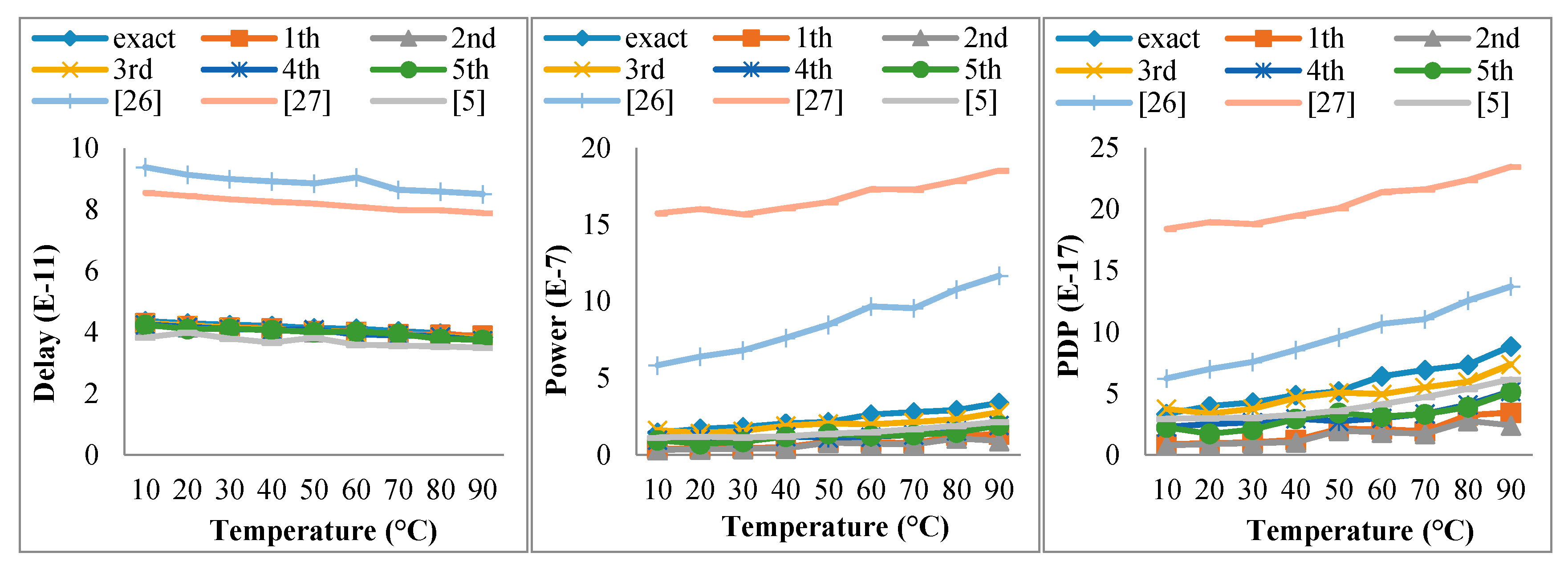
To asses the correct operation of the proposed methods and in comparison with previous state-of-the-art designs, all the methods are simulated for operational temperatures ranging from 0 °C to 90 °C at 200 MHz operational frequency and a 2 fF capacitor at output nodes. As Figure 8 shows, all of the proposed inexact methods benefit from lower delay and lower power consumption when compared to the previous exact multipliers.
Our designs along with the design of [5] are also more resilient to temperature variation, especially in their power and energy consumption. In contrast, the designs of [26,27] show increased power and energy consumption by increasing the temperature, which is because of their large number of transistors, which can be affected by temperature variation.
Figure 9 evaluates the correct operation of all circuits under various supply voltages. This figure represents the results at 200 MHz input frequency and a load capacitor of 2 fF. As anticipated, more supply voltages will result in more power consumption for all designs. The fifth proposed inexact design has almost 6X and 9X lower power consumption compared with designs of [26] and [27] at 0.9 V supply voltages, respectively.
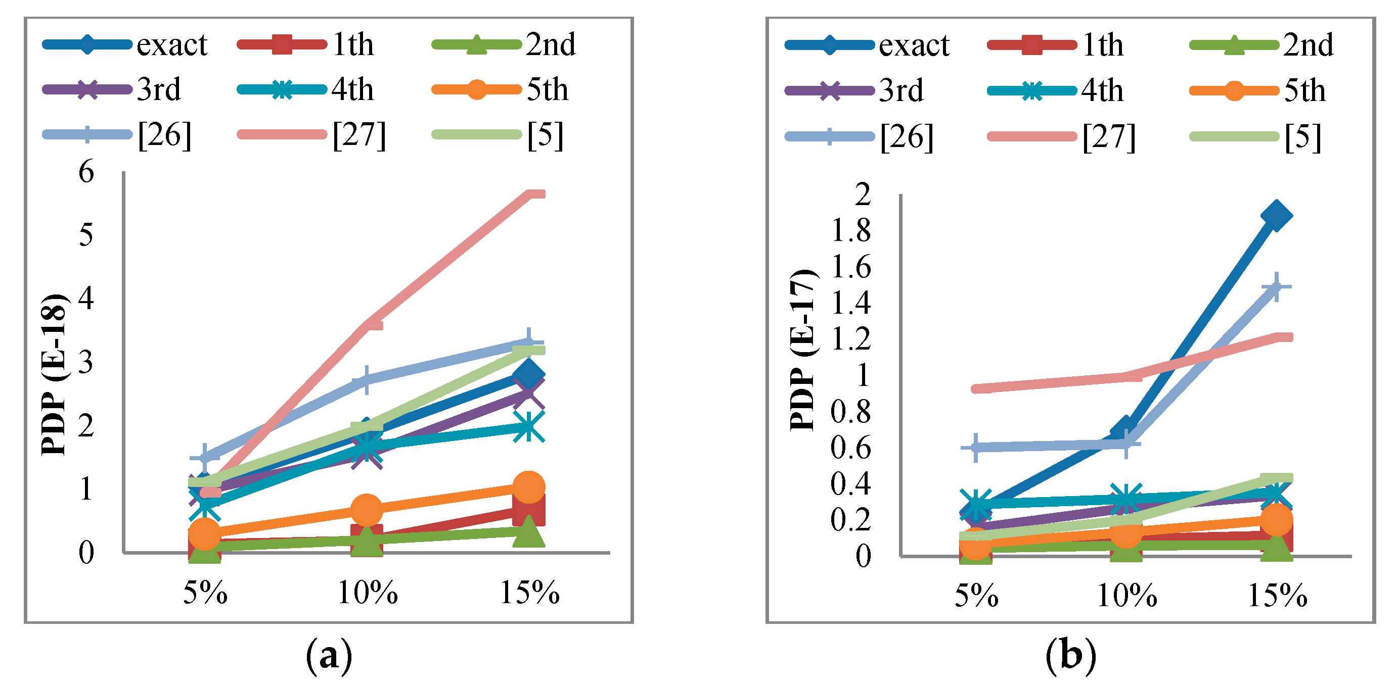
As we know, CNFETs have a large margin for process variations compared to MOSFETs. However, due to lithographic techniques and fabrication processes, they are prone to parametric variations such as variation in pitch value, number of tubes, or nanotube’s diameter [29]. Hence, designing a process-variation aware circuit is very important. The Monte Carlo simulation is conducted to identify the sensitivity of the proposed methods against diameter variation and density variation (pitch and number of tubes). The simulation of the proposed designs is conducted with up to under Gaussian distribution at . Figure 10 shows that the proposed methods are almost constant in PDP values by increasing the percentage of parameter variation compared to the existing designs. This is especially true for inexact designs. Present systems are more intricate and susceptible to failure, and therefore, designs that work correctly under process, voltage, and temperature variations are preferred.
5. Applications
Approximate computing is applied in cases when the exact result is hard to find, it does not exist, or the imprecise results are sufficient for the users [30]. For example, the perceptual limitation of human vision capabilities persuades designers to use approximate computing in this class of applications. In this section, the results of using exact and inexact multipliers in image processing applications will be discussed. A multiplier can be used for sharpening, smoothing, and image multiplication in image processing applications. Two images are blended into a single output image by multiplying two images pixel by pixel [31,32]. Each RGB value of a pixel is an integer in the range of [0,255], which can be represented with a six-digit ternary number. Inexact one-trit multipliers were utilized to multiply two ternary numbers digit by digit. The results will be imprecise, but these inexact circuits might not cause that much degradation in the quality. The rest of this section compares the proposed inexact methods in different image processing applications such as image multiplication or image filtering, to find the most desirable method among all the proposed designs. C++ codes in Microsoft Visual Studio implement the following image applications.
To have a perspective on the error of the proposed approximate multipliers, we calculate the inaccuracy of the designs under normalized error distance (NED) metric. NED is independent of the multiplier size, which is useful for assessing the reliability of designs, as is discussed further in [33]. NED is calculated based on Equation (5) [33].
where EDi is the difference between the output of precise block and the output of its imprecise version for i-th input vector, and D denotes the maximum possible of ED in an imprecise multiplier.
Table 7 shows NED values for the proposed inexact multipliers for a ternary multiplication. As anticipated, the first and the second methods that have inexact carry outputs have the highest error value, while the fifth method that is exact for more input conditions has the least NED value. For the exact proposed method and designs of [26,27], NED is zero since all of the multiplication results are equal to the exact result. To find a balance point between the error value and the power consumption of the designs, the metric of NED Power is defined and calculated for the imprecise designs in Table 7. The power value that is reported in this table is calculated for a 6 multiplication (excluding the reduction steps). By taking into account the NED Power values, it is concluded that the fifth method is the optimum design considering this metric.
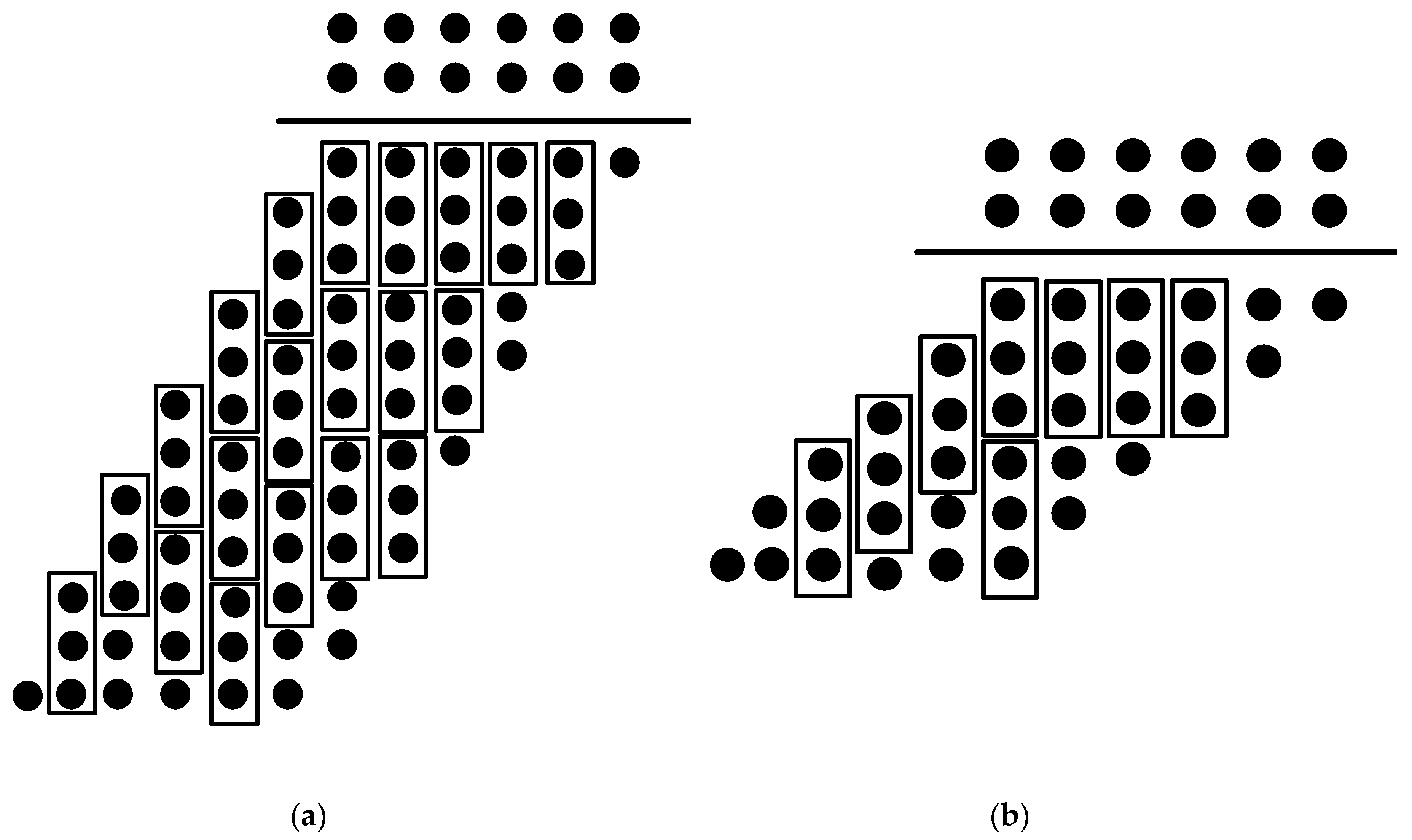
Figure 11 shows a 6 × 6 ternary multiplication steps that include six partial products with each one consisting of a product digit and a carry output digit. By ignoring the carry output, as it occurs in the first and the second inexact designs, the partial product digits will decrease by half, and consequently, the number of adder cells for the reduction steps will be reduced from 53 to 20. This is shown in Figure 11 for the first reduction step. But this is only one metric. The designs should be compared with other metrics, such as precision in various applications. The rest of the paper is dedicated to this subject.
One of the essential applications in image processing cases is the multiplication of two images. In this case, the peer-to-peer image pixels are multiplied into each other. The multiplication is a basic block and, therefore, its performance affects the overall performance of each application.
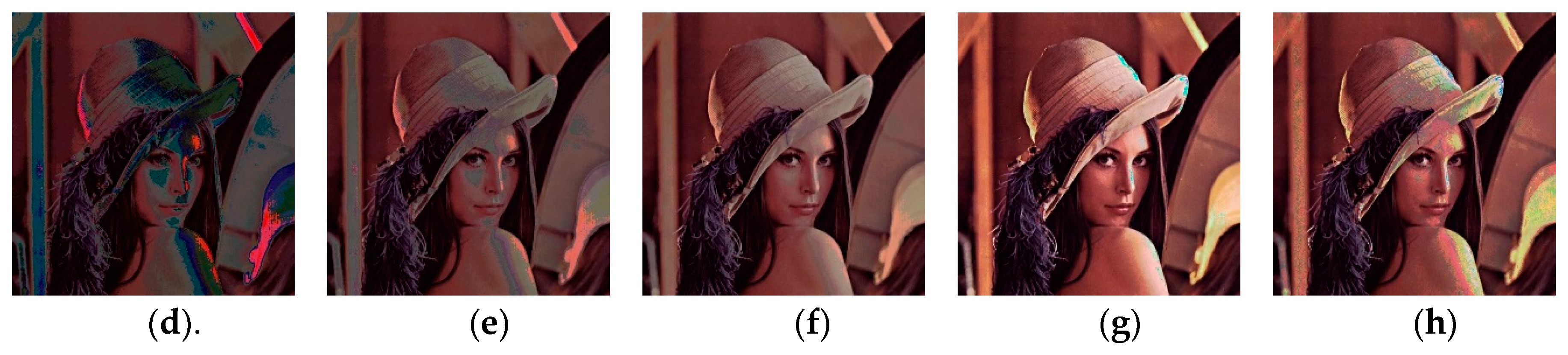
The proposed designs are utilized to examine the evaluation metrics with the intent to find a design that has the best operation that balances the error value and energy consumption. The results of an example of image multiplication have been shown in Figure 12. The inexact designs (except the first design) have an acceptable error value when compared to the exact ones which have a high energy consumption.
To evaluate the exactness of the image output results, we use PSNR (peak signal-to-noise ratio) is used as a quality measurement. This metric compares the degraded output image with the original image, which is the result of the exact multiplication. A higher PSNR value shows a more exact output. Table 7 shows the results of this example. As the PSNR values authenticate, the first inexact method, which has the most distance from the exact results, has the worst results. The fifth method is the best since, in this design, the probability of the exact output value is more than the other inexact proposed methods.
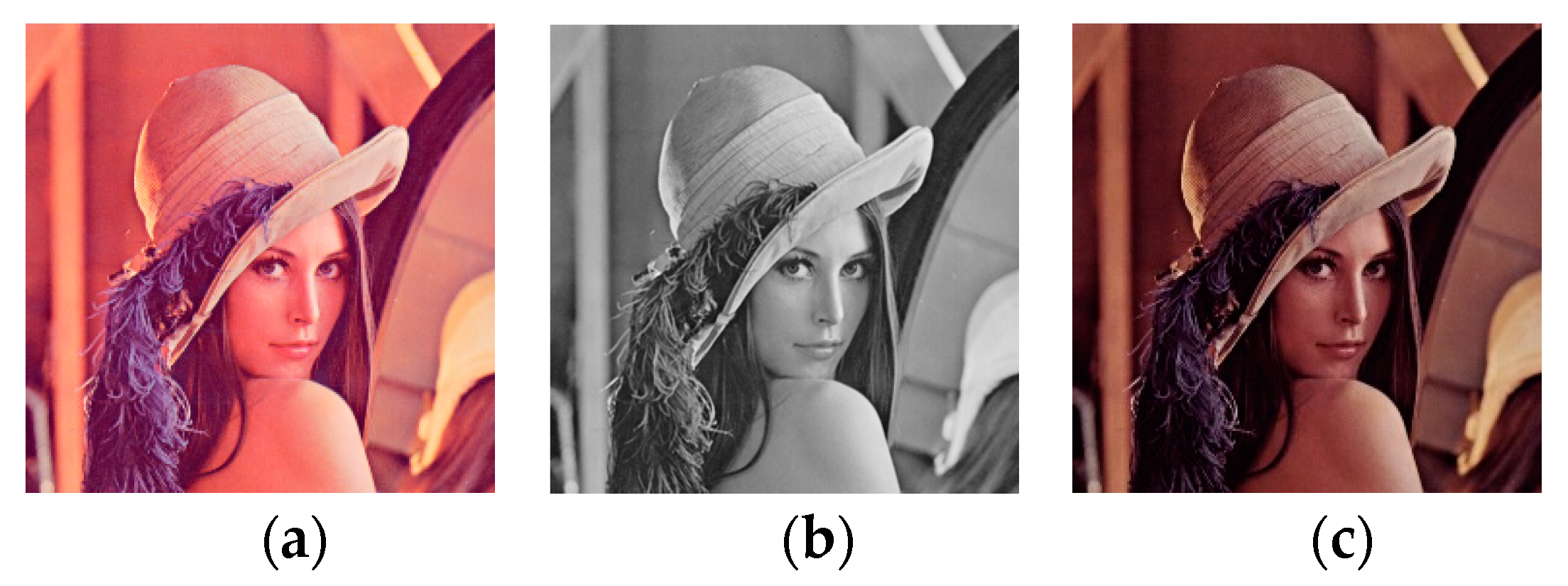
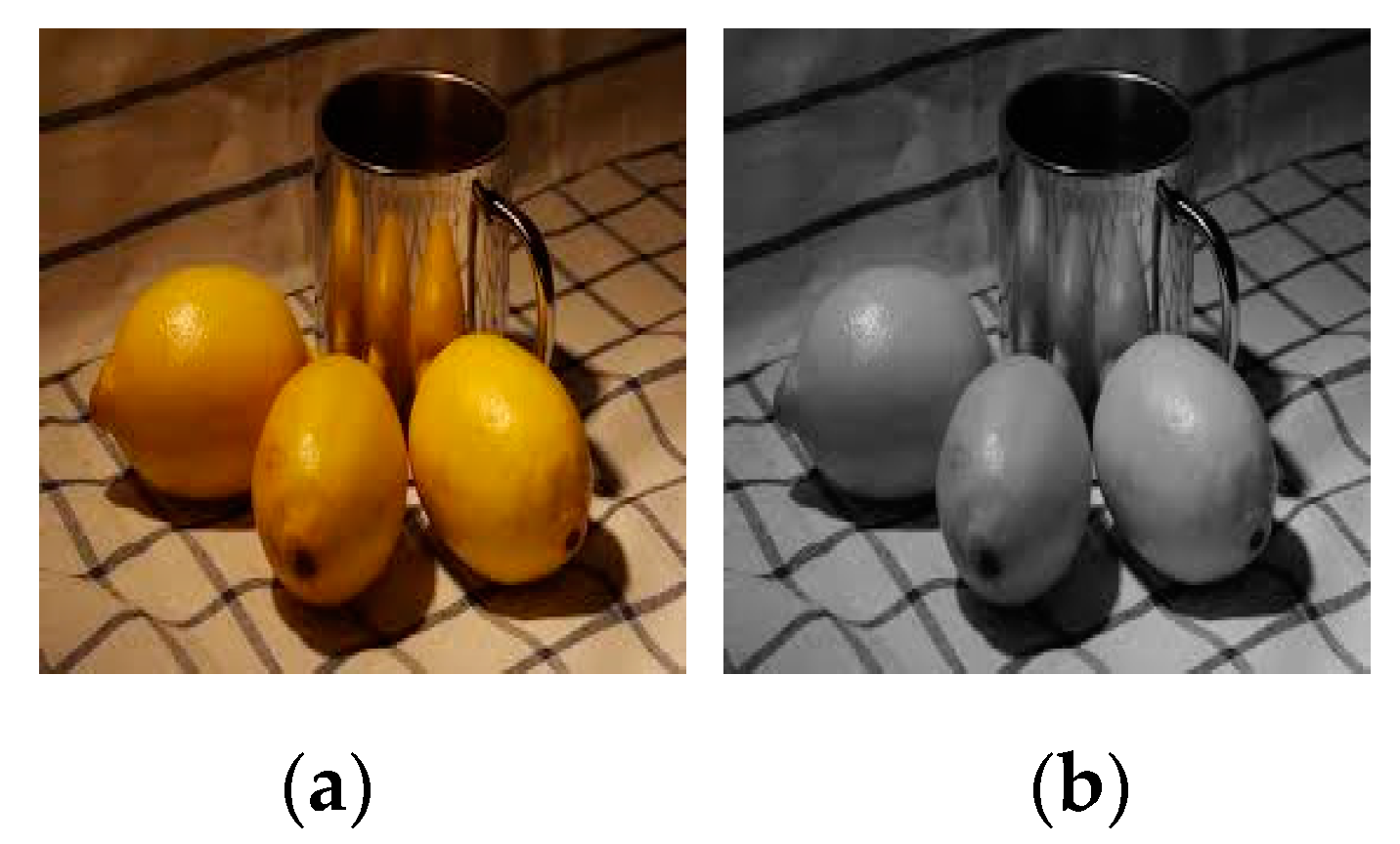
Another application that could be examined is the conversion of a color image to grayscale. By converting an image to grayscale, all of the RGB elements will be given the same value. This common value is calculated from a weighted average of the original RGB values of the input colored image [34]. The formula that is used to convert colored pixels to black and white is shown in (5) [34].
In this equation, , and are red, green and blue indices of the input image that construct the pixel’s color and , and are those of the grayscale output image.
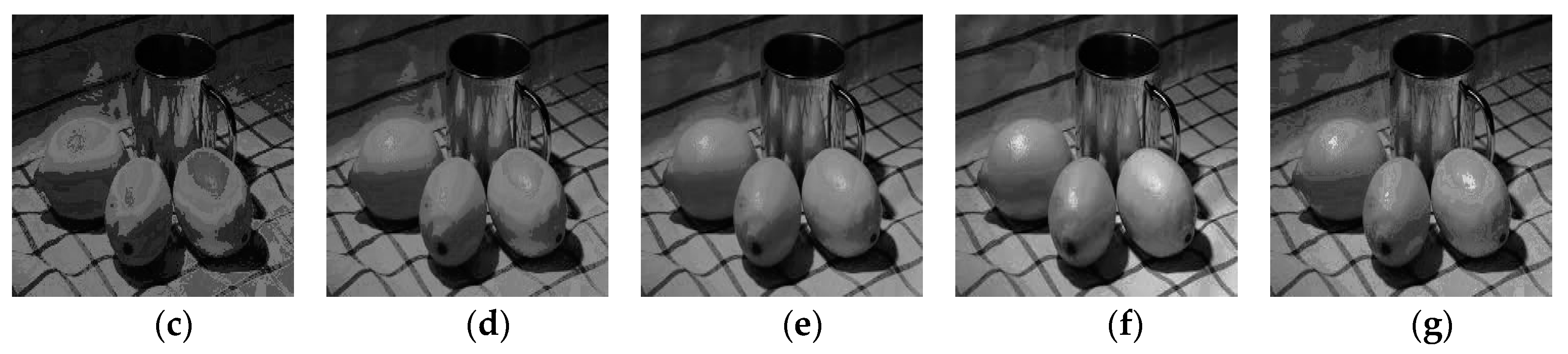
The proposed exact and approximate multipliers have been used in the multiplication of these values. As Figure 13 shows, all of the design’s results (except the first inexact design) have acceptable outputs, especially the fifth method, because its NED value is less than the others. PSNR values of this example are also shown in Table 8. In this example, the inexact designs do not have significant differences when compared to the exact design except the first design, which has lower PSNR value. PSNR metric shows this fact. Hence, imprecise designs are outstanding candidates that could be used instead of exact methods that have high power and delay. As Table 8 represents, the PSNR values of all inexact multipliers (except the first design) are acceptable for most of the application as it is mentioned in [35] that a typical PSNR value ranges between 20 dB to 40 dB.
These image processing applications are some of the thousands of applications in which an approximate multiplier could be utilized. Image and voice filtering, FFT algorithms, watermarking, and image reconstruction with NMF algorithms are some of those applications.
6. Conclusions
This paper proposed a new CNFET-based exact ternary one-digit multiplier which has better performance compared to the designs which use only one supply voltage. By considering the usefulness of a multiplier cell in image processing applications, inexact multipliers were proposed in this paper and have been utilized in some image processing applications. As the results show, the suggested approximate cells can be employed in DSP applications to have an energy-efficient design with an acceptable error value. We simulated all the proposed designs under different operational conditions. We compared the results of our designs with the previous methods. The results confirm the improvement of the proposed designs over the state-of-the-art designs in terms of energy efficiency.
Author Contributions
S.T. and A.P. did the designs of the circuits and did simulations. They also contributed to the writing of the initial draft of the paper. F.S. supervised the design of the circuits and the simulation. He also reviewed the results and took large part in writing the initial draft of the paper. H.M. and A.-H.A.B. were in advising roles. They contributed to improvements to the designs and also revised the various drafts of the paper. All authors have read and agreed to the published version of the manuscript.
Funding
This research received no external funding.
Conflicts of Interest
The authors declare no conflict of interest.
References
- Kish, L.B. End of Moor’s law: Thermal noise death of integration in micro and nanoelectronics. Phys. Lett. A 2002, 305, 144–149. [Google Scholar] [CrossRef]
- Chen, J.K.; Akeyoshi, T.; Maezawa, K. Monostable-bistable transition logic elements (MOBILEs) based on monolithic integration of resonant tunneling diodes and FETs. Jpn. J. Appl. Phys. 1995, 34, 1199. [Google Scholar] [CrossRef]
- Hadley, P.; Lientschnig, G.; Lai, M.-J. Single-electron transistors. Conf. Ser. Inst. Phys. 1999, 174, 125–132. [Google Scholar]
- Tahoori, M.B.; Huang, J.; Momenzadeh, M.; Lombardi, F. Testing of quantum cellular automata. IEEE Trans. Nanotechnol. 2004, 3, 432–442. [Google Scholar] [CrossRef]
- Shahrom, E.; Hosseini, S.A. A new low power multiplexer based ternary multiplier using CNTFETs. AEU Int. J. Electron. Commun. 2018, 93, 191–207. [Google Scholar] [CrossRef]
- Ding, L.; Zhang, Z.; Liang, S.; Pei, T.; Wang, S.; Li, Y.; Zhou, W.; Liu, J.; Peng, L.M. CMOS-based carbon nanotube pass transistor logic integrated circuits. Nat. Commun. 2012, 3, 1–7. [Google Scholar] [CrossRef] [Green Version]
- Tabrizchi, S.; Sharifi, F.; Badawy, A.-H.; Saifullah, Z. Enabling energy-efficient ternary logic gates using CNFETs. In Proceedings of the 2017 IEEE 17th International Conference on Nanotechnology (IEEE-NANO), Pittsburgh, PA, USA, 25–28 July 2017; pp. 542–547. [Google Scholar]
- Firouzi, S.; Tabrizchi, S.; Sharifi, F.; Badawy, A.H. High performance, variation-tolerant CNFET ternary full adder a process, voltage, and temperature variation-resilient design. Comput. Electr. Eng. 2019, 77, 205–216. [Google Scholar] [CrossRef]
- Smith, K.C. A multiple valued logic: A tutorial and appreciation. Computer 1988, 4, 17–27. [Google Scholar] [CrossRef]
- Hurst, S.L. Multiple-valued logic—Its status and future. IEEE Trans. Comput. 1984, 33, 1160–1179. [Google Scholar] [CrossRef]
- Hayes, B. Third base. Am. Sci. 2001, 89, 490–494. [Google Scholar] [CrossRef]
- Sharifi, F.; Saifullah, Z.; Badawy, A.-H. Design of adiabatic MTJ-CMOS hybrid circuits. In Proceedings of the 2017 IEEE 60th International Midwest Symposium on Circuits and Systems (MWSCAS), Boston, MA, USA, 6–9 August 2017; pp. 715–718. [Google Scholar]
- Han, J.; Orshansky, M. Approximate computing: An emerging paradigm for energy-efficient design. In Proceedings of the 18th IEEE European Test Symposium (ETS), Avignon, France, 27–30 May 2013; pp. 1–6. [Google Scholar]
- Lemme, M.C.; Echtermeyer, T.J.; Baus, M.; Kurz, H. A graphene field effect device. IEEE Electron Device Lett. 2007, 28, 282–284. [Google Scholar] [CrossRef] [Green Version]
- Martel, R.; Schmidt, T.; Shea, H.R.; Hertel, T.; Avouris, P. Single-and multi-wall carbon nanotube field-effect transistors. Appl. Phys. Lett. 1998, 73, 2447–2449. [Google Scholar] [CrossRef] [Green Version]
- Bachtold, A.; Hadley, P.; Nakanishi, T.; Dekker, C. Logic circuits with carbon nanotube transistors. Science 2001, 294, 1317–1320. [Google Scholar] [CrossRef]
- Sharifi, F.; Moaiyeri, M.H.; Navi, K.; Bagherzadeh, N. Robust and energy-efficient carbon nanotube FET-based MVL gates: A novel design approach. Microelectron. J. 2015, 46, 1333–1342. [Google Scholar] [CrossRef]
- O’Connor, I.; Liu, J.; Gaffiot, F.; Prégaldiny, F.; Lallement, C.; Maneux, C.; Goguet, J.; Frégonèse, S.; Zimmer, T.; Anghel, L.; et al. CNTFET modeling and reconfigurable logic-circuit design. IEEE Trans. Circuits Syst. I Regul. Pap. 2007, 54, 2365–2379. [Google Scholar] [CrossRef]
- Qin, L.-C. Determination of the chiral indices (n, m) of carbon nanotubes by electron diffraction. Phys. Chem. Chem. Phys. 2007, 9, 31–48. [Google Scholar] [CrossRef] [PubMed]
- Bok, K.Y.; Kim, Y.B.; Lombardi, F. Novel design methodology to optimize the speed and power of the CNTFET circuits. In Proceedings of the IEEE International Midwest Symp on Circuits and Systems, Cancun, Mexico, 2–5 August 2009; pp. 1130–1133. [Google Scholar]
- Tabrizchi, S.; Taheri, M.; Navi, K.; Bagherzadeh, N. Novel CNFET ternary circuit techniques for high-performance and energy-efficient design. IET Circuits Devices Syst. 2018, 13, 193–202. [Google Scholar] [CrossRef]
- Deng, J. Device Modeling and Circuit Performance Evaluation for Nanoscale Devices: Silicon Technology Beyond 45 nm Node and Carbon Nanotube Field-Effect Transistors. Ph.D. Thesis, Stanford University, Stanford, CA, USA, 2007. [Google Scholar]
- Deng, J.; Wong, H.-S.P. A compact SPICE model for carbon-nanotube field-effect transistors including non-idealities and its application-part I: Model of the intrinsic channel region. IEEE Trans. Electron Devices 2007, 54, 3186–3194. [Google Scholar] [CrossRef]
- Deng, J.; Wong, H.-S.P. A compact SPICE model for carbon-nanotube field-effect transistors including non-idealities and its application-part II: Full device model and circuit performance benchmarking. IEEE Trans. Electron Devices 2007, 54, 3195–3205. [Google Scholar] [CrossRef]
- Daraei, A.; Hosseini, S.A. Novel Energy-Efficient and High-Noise Margin Quaternary Circuits in Nanoelectronics. AEU Int. J. Electron. Commun. 2019, 105, 145–162. [Google Scholar] [CrossRef]
- Moaiyeri, M.H.; Dosstaregan, A.; Navi, K. Design of energy-efficient and robust ternary circuits for nanotechnology. IET Circuits Devices Syst. 2011, 5, 285–296. [Google Scholar] [CrossRef]
- Lin, S.; Kim, Y.-B.; Lombardi, F. CNTFET-based design of ternary logic gates and arithmetic circuits. IEEE Trans. Nanotechnol. 2011, 10, 217–225. [Google Scholar] [CrossRef]
- Mehrabani, Y.S.; Mirzaee, R.F.; Zareei, Z.; Daryabari, S.M. A novel high-speed, low-power CNTFET-based inexact full adder cell for image processing application of motion detector. J. Circuits Syst. Comput. 2017, 26, 1750082. [Google Scholar] [CrossRef]
- Paul, B.C.; Fujita, S.; Okajima, M.; Lee, T.H.; Wong, H.-P.; Nishi, Y. Impact of a process variation on nanowire and nanotube device performance. IEEE Trans. Electron Devices. 2007, 54, 2369–2376. [Google Scholar] [CrossRef]
- Venkatesan, R.; Agarwal, A.; Roy, K.; Raghunathan, A. MACACO: Modeling and analysis of circuits for approximate computing. In Proceedings of the International Conference on Computer-Aided Design, San Jose, CA, USA, 7–10 November 2011; IEEE: New York, NY, USA, 2011; pp. 667–673. [Google Scholar]
- Momeni, A.; Han, J.; Montuschi, P.; Lombardi, F. Design and analysis of approximate compressors for multiplication. IEEE Trans. Comput. 2015, 64, 984–994. [Google Scholar] [CrossRef]
- Akbari, O.; Kamal, M.; Afzali-Kusha, A.; Pedram, M. Dual-quality 4: 2 compressors for utilizing in dynamic accuracy configurable multipliers. IEEE Trans. Very Large Scale Integr. (VLSI) Syst. 2017, 25, 1352–1361. [Google Scholar] [CrossRef]
- Liang, J.; Han, J.; Lombardi, F. New metrics for the reliability of approximate and probabilistic adders. IEEE Trans. Comput. 2013, 62, 1760–1771. [Google Scholar] [CrossRef]
- Kumar, T.; Verma, K. A theory based on conversion of RGB image to gray image. Int. J. Comput. Appl. 2010, 7, 7–10. [Google Scholar] [CrossRef]
- Aggarwal, D.; Dhindsa, K.S. Effect of embedding watermark on compression of the digital images. J. Comput. 2010, 2, 5–8. [Google Scholar]
Figure 1.
Schematic design of the Out1 and Out2 output.

Figure 2.
Schematic design of the proposed exact multiplication digit.

Figure 3.
Schematic design of the proposed exact carry output digit.

Figure 4.
Transient responses of the proposed exact multiplier.

Figure 5.
Schematic design of the first proposed inexact design.

Figure 6.
Schematic design of the second proposed inexact design.

Figure 7.
Design of the fifth proposed inexact design.

Figure 8.
Operation of the proposed methods under temperature variation.

Figure 9.
Operation of the proposed methods under supply voltage variations.

Figure 10.
PDP variations vs. process variation of designs. (a) Carbon nanotube (CNT) diameter variation. (b) CNT density variation.
Figure 10.
PDP variations vs. process variation of designs. (a) Carbon nanotube (CNT) diameter variation. (b) CNT density variation.

Figure 11.
First Reduction step of a 6 6 ternary multiplication. (a) With exact carry. (b) With inexact carry.
Figure 11.
First Reduction step of a 6 6 ternary multiplication. (a) With exact carry. (b) With inexact carry.

Figure 12.
Image multiplication results. (a) First input. (b) Second input. (c) Exact design. (d) 1st design. (e) 2nd esign. (f) 3rd design. (g) 4th design. (h) 5th design.
Figure 12.
Image multiplication results. (a) First input. (b) Second input. (c) Exact design. (d) 1st design. (e) 2nd esign. (f) 3rd design. (g) 4th design. (h) 5th design.


Figure 13.
RGB to grayscale results. (a) Input image. (b) Exact output. (c) 1st design. (d) 2nd design. (e) 3rd design. (f) 4th design. (g) 5th design.
Figure 13.
RGB to grayscale results. (a) Input image. (b) Exact output. (c) 1st design. (d) 2nd design. (e) 3rd design. (f) 4th design. (g) 5th design.


Table 1.
Truth Table of One-Trit Ternary Multiplier.

Table 2.
Truth Table of Ternary NTI, PTI, Out1, and Out2.
| 0 | 2 | 2 | 2 | 0 |
| 1 | 0 | 2 | 0 | 2 |
| 2 | 0 | 0 | 2 | 0 |
Table 3.
Truth Table of inexact ternary multipliers.
| Inexact 1 | Inexact 2 | Inexact 3 | Inexact 4 | Inexact 5 | |||||||
|---|---|---|---|---|---|---|---|---|---|---|---|
| 0 | 0 | 0 | 0 | 0 | 0 | 0 | 0 | 0 | 0 | 0 | 0 |
| 0 | 1 | 0 | 0 | 0 | 0 | 0 | 0 | 0 | 0 | 0 | 0 |
| 0 | 2 | 0 | 0 | 0 | 0 | 0 | 0 | 0 | 0 | 0 | 0 |
| 1 | 0 | 0 | 0 | 0 | 0 | 0 | 0 | 0 | 0 | 0 | 0 |
| 1 | 1 | 1 | 0 | 1 | 0 | 1 | 0 | 1 | 0 | 1 | 0 |
| 1 | 2 | 2 | 0 | 2 | 0 | 2 | 0 | 2 | 0 | 2 | 0 |
| 2 | 0 | 0 | 0 | 0 | 0 | 0 | 0 | 0 | 0 | 0 | 0 |
| 2 | 1 | 2 | 0 | 2 | 0 | 2 | 0 | 2 | 0 | 2 | 0 |
| 2 | 2 | 0 | 0 | 2 | 0 | 0 | 1 | 2 | 1 | X | 1 |
Table 4.
Carbon-nanotube field-effect transistor (CNFET) Model Parameters.
| Parameter | Description | Value |
|---|---|---|
| Physical channel Length | 32 nm | |
| The mean free path in the intrinsic CNT channel | 100 nm | |
| The length of doped CNT drain-side extension region | 32 nm | |
| The length of doped CNT source-side extension region | 32 nm | |
| The thickness of the high-k top gate dielectric material | 1 nm | |
| The dielectric constant of high-k top gate dielectric material | 16 | |
| The Femi level’s doped S/D tube | 6 eV | |
| The coupling capacitor of the channel region and the substrate | 20 pF/m |
Table 5.
Simulation Results.
| Delay (ps) | Power (uW) | Energy (aJ) | |
|---|---|---|---|
| Proposed exact design | 42.3 | 4.16 | 17.6 |
| 1st inexact design | 41.4 | 0.92 | 3.8 |
| 2nd inexact design | 41.5 | 0.81 | 3.3 |
| 3rd inexact design | 41.7 | 3.60 | 15 |
| 4th inexact design | 41.2 | 2.03 | 8.3 |
| 5th inexact design | 41.5 | 1.97 | 8.2 |
| Design of [5] | 37.2 | 2.92 | 10.8 |
| Design of [26] | 90.1 | 12.90 | 116 |
| Design of [27] | 83.7 | 18.87 | 158 |
Table 6.
Area and Energy Results.
| Transistors | Width (nm) | Width × Energy (e-25mJ) | |
|---|---|---|---|
| Proposed exact design | 26 | 2600 | 442 |
| 1st inexact design | 16 | 1600 | 60.8 |
| 2nd inexact design | 14 | 1400 | 46.2 |
| 3rd inexact design | 22 | 2200 | 330 |
| 4th inexact design | 20 | 2000 | 166 |
| 5th inexact design | 20 | 2000 | 164 |
| Design of [5] | 23 | 2300 | 248 |
| Design of [26] | 80 | 8000 | 9304 |
| Design of [27] | 94 | 9400 | 148,614 |
Table 7.
Normalized error distance (NED) and Power Comparison.
| NED (× 10−4) | Power (× 10−6 W) | NED × Power (× 10−10) | |
|---|---|---|---|
| 1st inexact design | 4.55 | 3.312 | 15.06 |
| 2nd inexact design | 2.27 | 2.916 | 6.619 |
| 3rd inexact design | 1.13 | 12.96 | 14.64 |
| 4th inexact design | 0.63 | 7.308 | 4.604 |
| 5th inexact design | 0.25 | 7.092 | 1.773 |
Table 8.
Peak signal-to-noise ratio (PSNR) Values.
| Designs | PSNR (dB) | |
|---|---|---|
| Image Multiplication | RGB to Grayscale | |
| 1st design | (16.43, 19.85, 21.86) | (19.21, 19.21, 19.21) |
| 2nd design | (22.44, 25.85, 27.81) | (25.19, 25.19, 25.19) |
| 3rd design | (28.42, 31.78, 33.63) | (31.04, 31.04, 31.04) |
| 4th design | (28.04, 31.58, 33.31) | (31.17, 31.17, 31.17) |
| 5th design | (31.07, 32.29, 33.50) | (31.81, 31.81, 31.81) |
© 2020 by the authors. Licensee MDPI, Basel, Switzerland. This article is an open access article distributed under the terms and conditions of the Creative Commons Attribution (CC BY) license (http://creativecommons.org/licenses/by/4.0/).
Share and Cite
MDPI and ACS Style
Tabrizchi, S.; Panahi, A.; Sharifi, F.; Mahmoodi, H.; A. Badawy, A.-H. Energy-Efficient Ternary Multipliers Using CNT Transistors. Electronics 2020, 9, 643. https://doi.org/10.3390/electronics9040643
AMA Style
Tabrizchi S, Panahi A, Sharifi F, Mahmoodi H, A. Badawy A-H. Energy-Efficient Ternary Multipliers Using CNT Transistors. Electronics. 2020; 9(4):643. https://doi.org/10.3390/electronics9040643
Chicago/Turabian StyleTabrizchi, Sepehr, Atiyeh Panahi, Fazel Sharifi, Hamid Mahmoodi, and Abdel-Hameed A. Badawy. 2020. "Energy-Efficient Ternary Multipliers Using CNT Transistors" Electronics 9, no. 4: 643. https://doi.org/10.3390/electronics9040643
Note that from the first issue of 2016, this journal uses article numbers instead of page numbers. See further details here.