A Frequency and Radiation Pattern Combo-Reconfigurable Novel Antenna for 5G Applications and Beyond


1
Microwave and Antenna Research Group, Electrical Engineering Department, University of Engineering and Technology Peshawar, Peshawar 25120, Pakistan
2
United States Pakistan Centre for Advanced Studies in Energy (USPCASE), University of Engineering and Technology Peshawar, Peshawar 25120, Pakistan
3
College of Engineering, Al-Ain University UAE, Abu Dhabi 64141, UAE
*
Author to whom correspondence should be addressed.
Electronics 2020, 9(9), 1372; https://doi.org/10.3390/electronics9091372
Submission received: 12 July 2020
/
Revised: 28 July 2020
/
Accepted: 6 August 2020
/
Published: 25 August 2020
(This article belongs to the Special Issue Reconfigurable Antennas)
Abstract
:This paper presents a novel combo-reconfigurable architecture for the frequency and radiation patterning of a novel antenna system for future fifth-generation (5G) millimeter-wave mobile communication. The tuning system independently controls the frequency and radiation pattern shifts, without letting them affect each other. The proposed antenna consists of two patches, radiating at 28 GHz and 38 GHz. A negative-channel metal–oxide–semiconductor (NMOS) transistor was used as a switch for ON/OFF states. Frequency reconfiguration was controlled by switches SD1 and SD2, while pattern reconfigurability was achieved by SD3–SD18. The desired resonant frequencies of 28 GHz and 38 GHz were achieved by varying patch dimensions through the ON and OFF states of the SD1 and SD2 switches. Similarly, parasitic stubs on the ground are used to control surface currents, which results in pattern reconfiguration. The results were analyzed for 18 different combinations of the switch states. Adding/removing parasitic stubs and switches changed the beam steering angle (by 45° shift) from 0° to 180°, which modified the stub dimensions and changed the beam-width of the main lobe.
1. Introduction
The next generation of telecommunication networks (fifth-generation or 5G) will hit the market by the end of 2021, and will proceed to grow globally. In addition to speed enhancement, 5G is expected to generate a vast IoT (internet of things) ecosystem in which networks can meet the communication needs and expectations of billions of connected devices, with the required standards of speed, latency and cost [1]. 5G mobile communication systems will have a significant impact on modern technology by transmitting information via millimeter waves (mmWaves), and will be quicker, easier to manage, and more reliable than present cellular technology for technological reasons [1]. The frequency band planned for future 5G infrastructure and for meeting bandwidth requirements is expected to be 28 GHz/38 GHz for mobile [2] and 60 GHz/73 GHz for wireless communication [3]. Antennas are a strict elementary part in any wireless system scheme. A lot of research has been concerned with multiband antenna systems operating in millimeter-wave frequency bands, and has been extensively explored [4]. Numerous designs using multi-band methods have been adopted for the 5G millimeter-wave bands. In [5], a circular microstrip antenna with an elliptical slot at 28 GHz and 45 GHz was introduced. The proposed structure was investigated for configuring a specific absorption rate (SAR) for a unit cell (with an SAR value for 28 GHz of 1.25 W/kg, and 1.38 W/kg for 45 GHz), 1 × 4 array (SAR value at 28 GHz is 1.19 W/kg, at 34 GHz is 1.16 W/kg and at 45 GHz is 1.37 W/kg), and a 5G wearable antenna application. In [6], a multiple input multiple output (MIMO) antenna had three bands for ultra-wide band (UWB) functions, with one band notching an adjusted 5 GHz to stop the wireless local area network (WLAN) frequency. The design of a two-dimensional (2D) slot antenna worked only at 28 GHz, which contained eight essential elements in a 2 × 4 shape [7]. The cellular handset printed circuit board, (PCB) with four single band elements of a microstrip antenna on a low-cost substrate of FR-4 at 28 GHz, was used in [8]. An eight-element microstrip antenna array functioning at 28 GHz and 38 GHz for the next generation of 5G communications was previously investigated [9]. Reference [10] presented a massive MIMO for a 28 GHz and a 38 GHz antenna. In [11], the designs of eight dual-band MIMO antennas for upcoming smartphones were offered. The antenna had a size of 7 × 15.5 mm2 for 3.3–3.6 GHz and 4.8–5.0 GHz 5G bands. Reference [12] introduced an antenna consisting of a radiator with a triangular shape and exponentially declined edges. The monopole antenna had a condensed area of 10 × 12 mm2. A 2 × 2 MIMO antenna was shown, with an envelope correlation coefficient lower than 0.001. For the first time, as far as we know, this article has accommodated various approaches of mmWave 5G antennas for cellular smartphones [13].
The published literature [4,5,6,7,8,9,10,11,12,13] has reviewed and used variously shaped smart antennas and MIMO antenna systems with radiating patches, and every category has been associated with its own merits and shortcomings for a particular application. Although smart antennas are a powerful concept, the cost associated with the multiple radio frequency (RF) chains and additional digital signal processing (DSP) (an external beamforming network) resources can limit their use in many practical applications. Compared with conventional antennas, the use of reconfigurable antennas is another fascinating and exciting approach for wireless communications network technologies [14]. Moreover, a reconfigurable antenna provides cost-saving functionality, as well as weight, volume and maintenance/repair benefits [14]. This type of antenna helps to reconfigure not only the frequency bandwidth, but also the pattern of radiation and polarization. Reconfigurable antenna provides versatile architectures and agile frequency, using defined operating systems and cognitive radios to deal with multi-service, multi-standard, and multi-band operations, which can be expanded and reconfigured. To implement a dynamical response, they employ different mechanisms such as PIN diodes, varactors, radio-frequency microelectromechanical systems (RF-MEMS), field effect transistors (FETs), parasitic pixel layers, photoconductive elements, mechanical actuators, metamaterials, ferrites and liquid crystals. These mechanisms enable the intentional distribution of current over the antenna’s surface, facilitating the reversible modification of their properties.
Much of the literature has focused on tuning a single antenna property, rather than multiple properties. The effective length of the antenna and its operating frequency can be changed by adding or removing part of the antenna’s length through electronic, optical, mechanical, or other, means. For instance, an author changed the effective length of a monopole antenna using optical switches, which helped eliminate some of the switch and bias line effects that can occur with other kinds of switches [15]. A similar design approach was taken in [16]. In this case, a balanced dipole fabricated on high-resistivity silicon was equipped with two silicon photo-conducting switches. Using four PIN diodes, a researcher developed a reconfigurable printed dipole antenna to deliver three operating bands between 5.2 GHz and 5.8 GHz [17]. Others have applied the same approach to microstrip patches [18], microstrip dipoles [19] and Yagi antennas [20]. Radiating structures based on fractal shapes that share the same underlying principle have been studied by numerous researchers [21,22]. With the reflective surface physically removed and isolated from the primary feed, reflector antennas are a natural choice for applications that require radiation pattern reconfiguration independent of frequency. Reference [23] demonstrated an example of a radiation-reconfigurable reflector antenna by actively changing the structure of a mesh reflector. In its first embodiment, the reflector contour was changed manually in certain regions, which resulted in changes in beam shape and direction. Later, computer-controlled stepper motors were implemented to pull cables attached to specific points on the reflector mesh, to support automatic pattern reconfiguration [24]. More recently, a similar system for satellite applications was developed to expand capabilities endowed by changes in the system’s sub reflector, rather than its main reflector [25]. It is extremely challenging to separate an antenna’s frequency characteristics from its radiation characteristics. Indeed, this ability to independently select operating frequency, bandwidth and radiation pattern characteristics is the ultimate goal of reconfigurable antenna designers. Recently, several research groups achieved this kind of reconfigurability, here termed compound or hybrid reconfigurability. A few of the antennas previously discussed are already capable of separating, and of selectable impedance and radiation performance [26,27]. In [26], an annular slot antenna was used as both a frequency- and pattern-reconfigurable device. In [27], a resonant single-turn microstrip spiral antenna provided a broadside radiation operation at two different frequencies, and end-fire radiation characteristics at one of these frequencies. A Yagi-based approach, using reconfigurable slot-loaded parasitic elements as directors and reflectors, was presented in a prior work, supporting tilted or broadside beams at two separate frequencies [28]. In [29], a reconfigurable stacked microstrip antenna delivers a broadside circularly polarized beam at one frequency, and a dipole pattern at a lower frequency, for joint satellite and terrestrial operation.
Aiming at the challenge of controlling the resonant frequencies and direction of the main lobe at the particular angle of interest, this paper provides a suitable solution for rapid development in communication system configurations where the frequency and pattern of the system can be independently tuned within a single antenna. Our research aimed to provide a novel antenna system that can achieve frequency as well as pattern reconfigurability by changing the dimensions of the patch and stubs, respectively. The frequencies targeted here are 28 GHz and 38 GHz (as per Federal Communications Commission (FCC, Washington, DC, USA) standards/guidelines for 5G mobile communication technology [30]), with 360° of rotation in the main beam of the pattern for both the desired frequencies. Until now, no such reconfigurable structure has been cited in mmWave applications.
2. Proposed Antenna Design
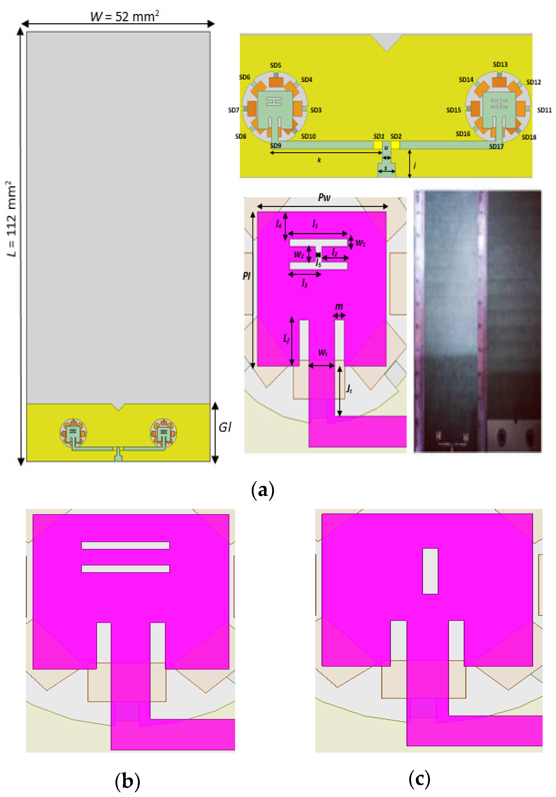
The geometric configuration of the proposed antenna is shown in Figure 1. The patch shows a vertically polarized antenna with respect to the feed line, which can be changed to horizontal polarization by varying its orientation. The proposed architecture was selected according to the standard dimensions of 5G cellular phablets. The circuit board was fabricated using a procedure of optic-radiation of photolithography, which processed the photoresist layer to paste the mask onto silicon sheets. The proposed antenna was designed in an Ansys HFSS (High Frequency Structure Simulator) 19.2 3D electromagnetic field simulator for the radio frequency and wireless design, and was measured using a ZVA 40 GHz vector network analyzer. A parametric analysis for the right choice was performed by introducing slots in the conducting patches of both 28 GHz and 38 GHz. To get multiple resonances, the analysis of gain and return loss was performed in accordance with the selection of the optimal model for the final results. As can be seen in Figure 2a,b, the return loss S11 (dB) and gain of different models led us to select model 1, which had a maximum S11 (dB) value (−39.2 dB for 28 GHz, an −38.9 dB for 38 GHz) and reasonable gains. The antenna designed for the nominated frequencies was a cheap and low-profile novel structure. The overall geometry consisted of two targeted frequencies—i.e., partial ground with connected stubs—and a substrate Rogers (Rogers Corporation, Chandler, AZ, USA) Duroid RT 5880, with dimensions of L × W × h = 112 × 52 × 0.508 mm3 (dielectric = 2.2, loss tangent ), where h denotes substrate thickness. The rest of the parameters, as shown in Table 1, were initially calculated via basic antenna equations [31] with respect to the selected resonant frequencies, i.e., 28 GHz and 38 GHz. The microstrip transmission line feeding technique was used to excite the antenna element (thickness of t = 0.035 mm).
In Figure 2, it can be seen that the return loss of model 1 is optimal as compared to the other models. This way of choosing optimal return loss is also a type of frequency reconfiguration.
In total, 10 negative-channel metal–oxide–semiconductor (NMOS) transistors were mounted on patched and partial ground. These NMOS transistors were used as RC (Resistor-Capacitor) equivalent circuits, as shown in Figure 3a, with a resistor (R) and capacitor (C) for ON/OFF states [32]. In order to validate the simulations, the proposed hybrid reconfigurable antenna was fabricated, manufactured or designed for ON/OFF states using PSPICE Software, as shown in Figure 3b.
While designing hybrid frequency and a radiation pattern-based antenna, the frequency response, with its related parameters, was considered, such as return loss (RL), voltage standing wave ratio (VSWR), reflection coefficient and a dominant TM (Transverse-Magnetic) mode based on cavity theory (Equations (1) and (2) [33]).
The stub radius (RS) with a fringing effect at frequencies of 28 GHz and 38 GHz was previously identified [34]:
where
3. Analytical Results and Discussion
In this section, we investigated the modeled antenna, using an Ansys high frequency structure simulator (Electromagnetics Suit, HFSS, Ansys, Canonsburg, PA, USA). We analyzed the measured and simulated results for the proposed antenna with return loss (VSWR), as well as the gain and efficiency steering at different modes and states for both 28 GHz and 38 GHz.
3.1. Frequency/VSWR/Bandwidth/Gain/Efficiency Reconfiguration Analysis
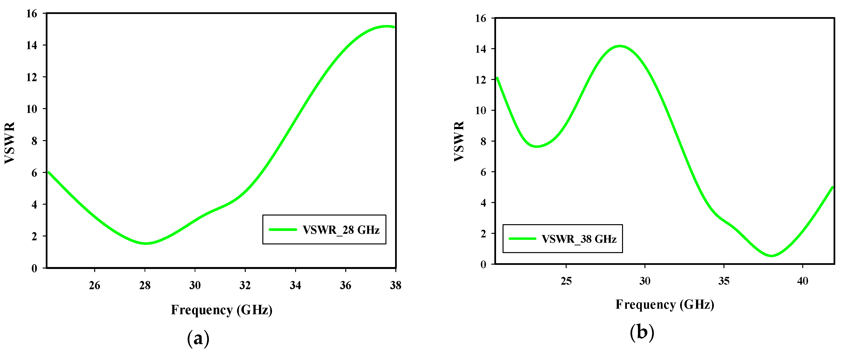
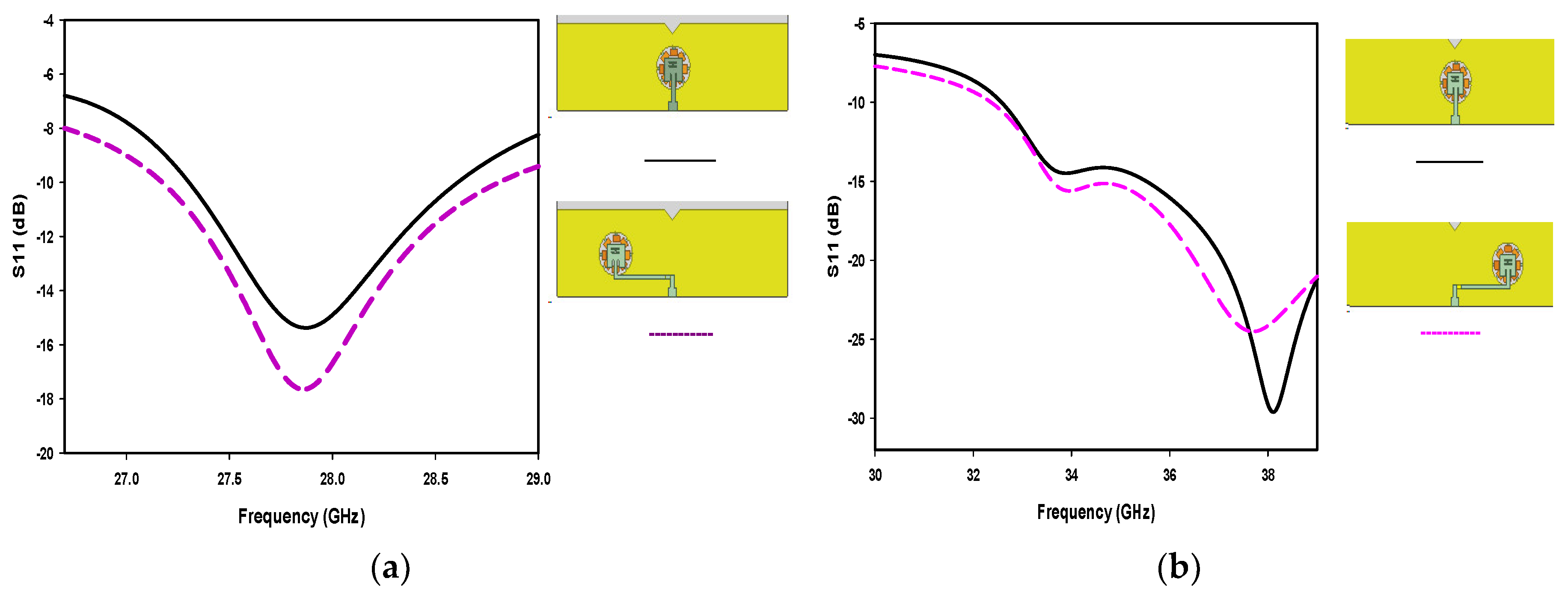
In this subsection, the frequency reconfigurability of the proposed model 1 was observed using two switches, i.e., SD1 and SD2. In Figure 4 and Table 4, it can be seen that when SD1 was ON and the other switches were OFF, the proposed antenna resonated at 28.10 GHz (simulated) and 28.66 GHz (measured). Similarly, a frequency of 37.63 GHz (simulated) and resonant frequency of 38.3 GHz (measured) was perceived when switch SD2 was in the ON state, while the rest of the switches were kept OFF, subjected to the unidirectional mmWaves of 5G mobile communication. Further, RL < −10 dB for both 28 GHz and 38 GHz mmWave frequency bands was the finite result of the simulations measured, with a small dissimilarity. These results were due to losses connected with SMA (Sub-Miniature version A), tangent loss, improper soldering and other environmental factors arising during the fabrication process. Figure 5 shows the simulated and measured VSWR for every state (from Table 2). The results show that, for State 2, the impedance bands were 1.4 GHz and 1.51 GHz for 28 GHz and 38 GHz (<2.5 standards, respectively).
While investigating the parametric models, the right structure was chosen and then analyzed individually for the return loss of selected frequencies, rather analyzing the whole design (Figure 6).
3.2. Radiation Pattern Reconfiguration Analysis
In this section, we discuss the pattern reconfiguration of different modes presented in Table 3. For pattern steering, parasitic stubs were connected with partial ground through NMOS switches (SD1–SD18). The purpose of these switches was to yield the change in surface current distribution, which would thus change the characteristics of the radiation patterning. As a result, the radiation pattern and surface current density of the antenna operating at different switching modes was derived as 45° shift along the XOY-plane (E-plane) at . This direction along the XOY-plane was altered by changing the ON-OFF state in SD1–SD18. In accordance with the ON-OFF states of the parasitic stubs with symmetrical antenna structures, the single main beam’s direction was symmetrically variant along the z-axis in the XOY-plane (Figure 7, from mode 1–mode 16). These modes showed narrow HPBW (Half Power Beamwidth) and a high-quality pattern.
Figure 7 shows the co- and cross (X) polarization radiation pattern results from Table 3 (from mode 1 to 16). It illustrates that from mode 1 to 8, SD1 is ON and SD2 is OFF (SD1 and SD2 are the main cause of frequency reconfiguration), operating with a resonant frequency of 28 GHz (it is unconcerned with 38 GHz). In this case, connecting the parasitic stubs from SD3 to SD10 assists in the radiation shift of the main lobe at the 28 GHz frequency. As you can see in Figure 7, the changing positions of the pattern (anti-clockwise) cause the surface current density to vary, due to the connecting parasitic stubs. Depending on the number of stubs, we can increase/decrease the steering angle (45° shift is used in this paper). Similarly, from mode 9 to 16, SD1 is OFF and SD2 is ON, which results in a 38 GHz resonant frequency. In this case, stubs being connected from SD11 to SD18, as shown in Figure 7, aids in the radiation pattern reconfiguration at 38 GHz. The novelty is that both the frequencies are controlled irrespective of each other.
Our investigation results were compared with the previously published literature, as shown in Table 5. The major attributes of the proposed model are as follows:
- (a)
- This structure was a novel design for mmWaves, never claimed before.
- (b)
- Frequency and pattern were independently controlled in a single antenna, showing structural novelty.
4. Conclusions
In this paper, a combination of frequency and radiation pattern reconfiguration was presented for an antenna system designed for 5G applications and beyond. The proposed antenna was fabricated for 5G mmWave mobile communication at 28 GHz and 38 GHz. In total, 18 NMOS transistors were used as switches for the ON and OFF states. Two switches, SD1 and SD2, were used for frequency tuning, while the other switches were utilized for pattern steering at different angles, in 45° steps, with the targeted resonant frequencies (28 GHz and 38 GHz). The steering angle is totally dependent on the number of parasitic stubs mounted on the partial ground in the proposed design, and can be altered by varying the number of stubs. The proposed model is a novel structure and can be used for future 5G mobile communication applications.
Author Contributions
M.K.S. provided the idea, performed the experiments and managed the paper. M.I.K. conceived of the presented idea, verified the analytical methods contributed to the interpretation of the results and took the lead in writing the manuscript. M.A.-H. assisted in the idea development and paper writing. All authors discussed the results and contributed to the final manuscript. All authors have read and agreed to the published version of the manuscript.
Funding
This work is funded in part by the Abu-Dhabi Department of Education and Knowledge (ADEK) Award for Research Excellence 2019 under Grant AARE19-245.
Conflicts of Interest
The authors declare no conflict of interest.
References
- Haris, R.M.; Al-Maadeed, S. Integrating Blockchain Technology in 5G enabled IoT: A Review. In Proceedings of the 2020 IEEE International Conference on Informatics, IoT, and Enabling Technologies (ICIoT), Doha, Qatar, 2–5 February 2020; pp. 367–371. [Google Scholar] [CrossRef]
- Chettri, L.; Bera, R. A Comprehensive Survey on Internet of Things (IoT) Toward 5G Wireless Systems. IEEE Internet Things J. 2020, 7, 16–32. [Google Scholar] [CrossRef]
- Liu, Y.; Li, Y.; Ge, L.; Wang, J.; Ai, B. A Compact Hepta-Band Mode-Composite Antenna for Sub (6, 28, and 38) GHz Applications. IEEE Trans. Antennas Propag. 2020, 68, 2593–2602. [Google Scholar] [CrossRef]
- Shereen, M.K.; Khattak, M.I.; Witjaksono, G. A brief review of frequency, radiation pattern, polarization, and compound reconfigurable antennas for 5G applications. J. Comput. Electron. 2019, 18, 1065–1102. [Google Scholar] [CrossRef]
- Khattak, M.I.; Sohail, A.; Khan, U.; Ullah, Z.; Witjaksono, G. Elliptical Slot Circular Patch Antenna Array with Dual Band Behaviour for Future 5G Mobile Communication Networks. Prog. Electromagn. Res. C 2019, 89, 133–147. [Google Scholar] [CrossRef] [Green Version]
- Kumar, A.; Ansari, A.Q.; Kanaujia, B.K.; Kishor, J.; Tewari, N. Design of triple-band MIMO antenna with one band-notched characteristic. Prog. Electromagn. Res. C 2018, 86, 41–53. [Google Scholar] [CrossRef] [Green Version]
- Alreshaid, A.T.; Hammi, O.; Sharawi, M.S.; Sarabandi, K. A compact millimeter-wave slot antenna array for 5G standards. In Proceedings of the 2015 IEEE 4th Asia-Pacific Conference on Antennas and Propagation (APCAP), Kuta, Indonesia, 30 June–3 July 2015; pp. 84–85. [Google Scholar] [CrossRef]
- Ali, M.M.M.; Sebak, A.-R. Directive antennas for future 5G mobile wireless communications. In Proceedings of the General Assembly and Scientific Symposium of the International Union of Radio Science (URSI GASS), Montreal, QC, Canada, 19–26 August 2017; pp. 1–4. [Google Scholar] [CrossRef]
- Ashraf, N.; Haraz, O.M.; Ali, M.M.M.; Ashraf, M.A.; Alshebili, S.A.S. Optimized broadband and dual-band printed slot antennas for future millimeter wave mobile communication. Aeuinternational J. Electron. Commun. 2016, 70, 257–264. [Google Scholar] [CrossRef]
- Ali, M.M.M.; Sebak, A.-R. Design of compact millimeter wave massive MIMO dual-band (28/38 GHz) antenna array for future 5G communication systems. In Proceedings of the 2016 17th International Symposium on Antenna Technology and Applied Electromagnetics (ANTEM), Montreal, QC, Canada, 10–13 July 2016; pp. 1–2. [Google Scholar] [CrossRef]
- Yan, K.; Yang, P.; Yang, F.; Zeng, L.; Huang, S. Eight-antenna array in the 5G smartphone for the dual-band MIMO system. In Proceedings of the 2018 IEEE International Symposium on Antennas and Propagation & USNC/URSI National Radio Science Meeting, Boston, MA, USA, 8–13 July 2018; pp. 41–42. [Google Scholar] [CrossRef]
- Hasan, M.N.; Seo, M. Compact omnidirectional 28GHz 2 × 2 MIMO antenna array for 5G communications. In Proceedings of the 2018 International Symposium on Antennas and Propagation (ISAP), Busan, Korea, 23–26 October 2018; pp. 1–2. [Google Scholar]
- Hong, W.; Baek, K.-H.; Ko, S. Millimeter-wave 5G antennas for smartphones: Overview and experimental demonstration. IEEE Trans. Antennas Propag. 2017, 65, 6250–6261. [Google Scholar] [CrossRef]
- Christodoulou, C.G.; Tawk, Y.; Lane, S.A.; Erwin, S.R. Reconfigurable Antennas for Wireless and Space Applications. Proc. IEEE 2012, 100, 2250–2261. [Google Scholar] [CrossRef]
- Freeman, J.L.; Lamberty, B.J.; Andrews, G.S. Optoelectronically reconfigurable monopole antenna. Electron. Lett. 1992, 28, 1502–1503. [Google Scholar] [CrossRef]
- Panagamuwa, C.J.; Chauraya, A.; Vardaxoglou, J.C. Frequency and beam reconfigurable antenna using photoconducting switches. IEEE Trans. Antennas Propag. 2006, 54, 449–454. [Google Scholar] [CrossRef] [Green Version]
- Roscoe, D.J.; Shafai, L.; Ittipiboon, A.; Cuhaci, M.; Douville, R. Tunable dipole antennas. In Proceedings of the IEEE/URSI International Symposium on Antennas and Propagation, Ann Arbor, MI, USA, 28 June–2 July 1993; pp. 672–675. [Google Scholar] [CrossRef]
- Weedon, W.; Payne, W.; Rebeiz, G.; Herd, J.; Champion, M. MEMS-switched reconfigurable multi-band antenna: Design and modeling. In Proceedings of the IEEE Antennas and Propagation Society International Symposium. 1999 Digest. Held in conjunction with: USNC/URSI National Radio Science Meeting (Cat. No.99CH37010), Orlando, FL, USA, 11–16 July 1999; Volume 1, pp. 203–231. [Google Scholar]
- Brown, E.R. On the gain of a reconfigurable-aperture antenna. IEEE Trans. Antennas Propag. 2001, 49, 1357–1362. [Google Scholar] [CrossRef]
- Ali, M.A.; Wahid, P. A reconfigurable Yagi array for wireless applications. In Proceedings of the IEEE/URSI International Symposium on Antennas and Propagation, San Antonio, TX, USA, 16–21 June 2002; pp. 466–468. [Google Scholar] [CrossRef]
- Vinoy, K.; Varadan, V. Design of reconfigurable fractal antennas and RF-MEMS for space-based systems. Smart Mater. Struct. 2001, 10, 1211–1223. [Google Scholar] [CrossRef]
- Anagnostou, D.E.; Zheng, G.; Chryssomallis, M.T.; Lyke, J.C.; Ponchak, G.E.; Papapolymerou, J.; Christodoulou, C.G. Design, fabrication, and measurements of an RFMEMS-based self-similar reconfigurable antenna. IEEE Trans. Antennas Propag. 2006, 54, 422–432. [Google Scholar] [CrossRef]
- Clarricoats, P.J.B.; Zhou, H. The design and performance of a reconfigurable mesh reflector antenna. IEE Digit. Libr. 1991, 138, 485–492. [Google Scholar]
- Clarricoats, P.J.B.; Zhou, H.; Monk, A. Electronically controlled reconfigurable reflector antenna. In Proceedings of the Antennas and Propagation Society Symposium 1991 Digest, London, ON, Canada, 24–28 June 1991; pp. 179–181. [Google Scholar] [CrossRef]
- Washington, G.; Yoon, H.S.; Angelino, M.; Theunissen, W.H. Design, modeling, and optimization of mechanically reconfigurable aperture antennas. IEEE Trans. Antennas Propag. 2002, 50, 628–637. [Google Scholar] [CrossRef]
- Nikolaou, S.; Bairavasubramanian, R.; Lugo, C., Jr.; Carrasquillo, I.; Thompson, D.C.; Ponchak, G.E.; Papapolymerou, J.; Tentzeris, M.M. Pattern and frequency reconfigurable annular slot antenna using PIN diodes. IEEE Trans. Antennas Propag. 2006, 54, 439–448. [Google Scholar] [CrossRef]
- Huff, G.H.; Feng, J.; Zhang, S.; Bernhard, J.T. A novel radiation pattern and frequency reconfigurable single turn square spiral microstrip antenna. IEEE Microw. Wirel. Compon. Lett. 2003, 13, 57–59. [Google Scholar] [CrossRef]
- Yang, X.-S.; Wang, B.Z.; Wu, W.; Xiao, S. Yagi patch antenna with dual-band and pattern reconfigurable characteristics. IEEE Antennas Wirel. Propag. Lett. 2007, 6, 168–171. [Google Scholar] [CrossRef]
- Ali, M.; Sayem, A.T.M.; Kunda, V.K. A reconfigurable stacked microstrip patch antenna for satellite and terrestrial links. IEEE Trans. Veh. Technol. 2007, 56, 426–435. [Google Scholar] [CrossRef] [Green Version]
- Qamar, F.; Siddiqui, M.H.S.; Dimyati, K.; Noordin, K.A.B.; Majed, M.B. Channel characterization of 28 and 38 GHz MM-wave frequency band spectrum for the future 5G network. In Proceedings of the 2017 IEEE 15th Student Conference on Research and Development (SCOReD), Putrajaya, Malaysia, 13–14 December 2017; pp. 291–296. [Google Scholar] [CrossRef]
- Stutzman, W.L.; Thiele, G.A. Antenna Theory and Design; John Wiley & Sons: Hoboken, NJ, USA, 2012. [Google Scholar]
- Yasir, I.A.A.; Hasanain, A.H.A.; Baha, A.S.; Parchin, N.O.; Ahmed, M.A.; Abdulkareem, S.A.; Raed, A.A. New Radiation Pattern-Reconfigurable 60-GHz Antenna for 5G Communications; IntechOpen: London, UK, 2019. [Google Scholar] [CrossRef] [Green Version]
- Robert, E.C. Foundation for Microwave Engineering, 2nd ed.; John Wiley & Sons: Hoboken, NJ, USA, 1966. [Google Scholar]
- George, H.; Joseph, C. Practical Antenna Handbook 5/e; McGraw-Hill: New York, NY, USA, 2011. [Google Scholar]
- Chitra, R.J.; Nagarajan, V. Frequency reconfigurable antenna using PIN diodes. In Proceedings of the 2014 Twentieth National Conference on Communications (NCC), Kanpur, India, 28 February–2 March 2014; pp. 1–4. [Google Scholar] [CrossRef]
- Yamagajo, T.; Koga, Y. Frequency reconfigurable antenna with MEMS switches for mobile terminals. In Proceedings of the 2011 IEEE-APS Topical Conference on Antennas and Propagation in Wireless Communications, Torino, Italy, 12–16 September 2011; pp. 1213–1216. [Google Scholar] [CrossRef]
- Tian, H.; Jiang, L.J.; Itoh, T. A Compact Single-Element Pattern Reconfigurable Antenna with Wide-Angle Scanning Tuned by a Single Varactor. Prog. Electromagn. Res. C 2019, 92, 137–150. [Google Scholar] [CrossRef] [Green Version]
- Kang, W.; Lee, S.; Kim, K. A pattern-reconfigurable antenna using PIN diodes. Microw. Opt. Technol. Lett. 2011, 53, 1883–1887. [Google Scholar] [CrossRef]
- Li, W.; Ren, Z.; Shi, X.; Hei, Y. A frequency and pattern reconfigurable microstrip antenna using PIN diodes. In Proceedings of the IEEE Antennas and Propagation Society International Symposium (APSURSI), Memphis, TN, USA, 6–11 July 2014; pp. 1449–1450. [Google Scholar] [CrossRef]
- Ghaffar, A.; Li, X.J.; Hussain, N.; Awan, W.A. Flexible Frequency and Radiation Pattern Reconfigurable Antenna for Multi-Band Applications. In Proceedings of the 2020 4th Australian Microwave Symposium (AMS), Sydney, Australia, 13–14 February 2020; pp. 1–2. [Google Scholar] [CrossRef]
- Li, P.K.; Shao, Z.H.; Wang, Q.; Cheng, Y.J. Frequency- and pattern-reconfigurable antenna for multistandard wireless applications. IEEE Antennas Wirel. Propag. Lett. 2015, 14, 333–336. [Google Scholar] [CrossRef]
- Majid, H.A.; Rahim, M.K.A.; Hamid, M.R.; Ismail, M.F. Frequency and pattern reconfigurable slot antenna. IEEE Trans. Antennas Propag. 2014, 62, 5339–5343. [Google Scholar] [CrossRef]
Figure 1.
Proposed antenna (a) model 1; (b) patch of model 2; (c) patch of model 3.

Figure 2.
Investigation for parametric analysis. (a) Return loss of different models (State 1 of Table 2); (b) gain investigation for parametric analysis of different models.
Figure 2.
Investigation for parametric analysis. (a) Return loss of different models (State 1 of Table 2); (b) gain investigation for parametric analysis of different models.

Figure 3.
(a) Equivalent circuit for ON/OFF states in a negative-channel metal–oxide–semiconductor (NMOS) transistor; (b) circuitry for NMOS switch co-simulation for mode 1 (Table 3) of the proposed antenna.
Figure 3.
(a) Equivalent circuit for ON/OFF states in a negative-channel metal–oxide–semiconductor (NMOS) transistor; (b) circuitry for NMOS switch co-simulation for mode 1 (Table 3) of the proposed antenna.

Figure 4.
(a) State 1, (b) State 2 and (c) State 3. Return loss at different states of Table 2.
Figure 4.
(a) State 1, (b) State 2 and (c) State 3. Return loss at different states of Table 2.

Figure 5.
VSWR at (a) State 2 and (b) State 3 of Table 2.
Figure 5.
VSWR at (a) State 2 and (b) State 3 of Table 2.

Figure 6.
Parametric analysis of individual patches for (a) 28 GHz and (b) 38 GHz.

Figure 7.
Co- and cross (X) polarization results showing radiation pattern of both 28 GHz and 38 GHz on XOY-E-Plane at different modes from Table 3.
Figure 7.
Co- and cross (X) polarization results showing radiation pattern of both 28 GHz and 38 GHz on XOY-E-Plane at different modes from Table 3.


Table 1.
Parameters and their dimensions.
| Parameter | Dimension (mm) | Parameter | Dimension (mm) |
|---|---|---|---|
| 3 | 0.3 | ||
| 12.5 | 0.4 | ||
| 2 | 0.2 | ||
| 1.8 | 1.2 | ||
| 0.2 | 0.8 | ||
| 0.8 | 5.5 | ||
| 0.3 | 5.2 | ||
| 0.2 | 0.3 | ||
| 1.5 | 4 | ||
| 0.035 | 3.8 | ||
| 4 | 2 | ||
| 3.8 | 1.9 | ||
| 15 | 1 |
Table 2.
State simulation statuses and directions.
| State | SD1 | SD2 | All Other Switches | Direction |
|---|---|---|---|---|
| State 1 | ON | ON | OFF | Pattern is directed in the middle |
| State 2 | ON | OFF | OFF | Uni-directional |
| State 3 | OFF | ON | OFF | Uni-directional |
Table 3.
Different operational modes for pattern reconfiguration.
| Mode | SD1 | SD2 | SD3 | SD4 | SD5 | SD6 | SD7 | SD8 | SD9 | SD10 | SD11 | SD12 | SD13 | SD14 | SD15 | SD16 | SD17 | SD18 |
|---|---|---|---|---|---|---|---|---|---|---|---|---|---|---|---|---|---|---|
| 1 | ON | OFF | ON | OFF | OFF | OFF | OFF | OFF | OFF | OFF | OFF | OFF | OFF | OFF | OFF | OFF | OFF | OFF |
| 2 | ON | OFF | OFF | ON | OFF | OFF | OFF | OFF | OFF | OFF | OFF | OFF | OFF | OFF | OFF | OFF | OFF | OFF |
| 3 | ON | OFF | OFF | OFF | ON | OFF | OFF | OFF | OFF | OFF | OFF | OFF | OFF | OFF | OFF | OFF | OFF | OFF |
| 4 | ON | OFF | OFF | OFF | OFF | ON | OFF | OFF | OFF | OFF | OFF | OFF | OFF | OFF | OFF | OFF | OFF | OFF |
| 5 | ON | OFF | OFF | OFF | OFF | OFF | ON | OFF | OFF | OFF | OFF | OFF | OFF | OFF | OFF | OFF | OFF | OFF |
| 6 | ON | OFF | OFF | OFF | OFF | OFF | OFF | ON | OFF | OFF | OFF | OFF | OFF | OFF | OFF | OFF | OFF | OFF |
| 7 | ON | OFF | OFF | OFF | OFF | OFF | OFF | OFF | ON | OFF | OFF | OFF | OFF | OFF | OFF | OFF | OFF | OFF |
| 8 | ON | OFF | OFF | OFF | OFF | OFF | OFF | OFF | OFF | ON | OFF | OFF | OFF | OFF | OFF | OFF | OFF | OFF |
| 9 | OFF | ON | OFF | OFF | OFF | OFF | OFF | OFF | OFF | OFF | ON | OFF | OFF | OFF | OFF | OFF | OFF | OFF |
| 10 | OFF | ON | OFF | OFF | OFF | OFF | OFF | OFF | OFF | OFF | OFF | ON | OFF | OFF | OFF | OFF | OFF | OFF |
| 11 | OFF | ON | OFF | OFF | OFF | OFF | OFF | OFF | OFF | OFF | OFF | OFF | ON | OFF | OFF | OFF | OFF | OFF |
| 12 | OFF | ON | OFF | OFF | OFF | OFF | OFF | OFF | OFF | OFF | OFF | OFF | OFF | ON | OFF | OFF | OFF | OFF |
| 13 | OFF | ON | OFF | OFF | OFF | OFF | OFF | OFF | OFF | OFF | OFF | OFF | OFF | OFF | ON | OFF | OFF | OFF |
| 14 | OFF | ON | OFF | OFF | OFF | OFF | OFF | OFF | OFF | OFF | OFF | OFF | OFF | OFF | OFF | ON | OFF | OFF |
| 15 | OFF | ON | OFF | OFF | OFF | OFF | OFF | OFF | OFF | OFF | OFF | OFF | OFF | OFF | OFF | OFF | ON | OFF |
| 16 | OFF | ON | OFF | OFF | OFF | OFF | OFF | OFF | OFF | OFF | OFF | OFF | OFF | OFF | OFF | OFF | OFF | ON |
Table 4.
Bandwidth (BW), gain, efficiency and voltage standing wave ratio (VSWR) analysis at different states for frequency reconfiguration.
Table 4.
Bandwidth (BW), gain, efficiency and voltage standing wave ratio (VSWR) analysis at different states for frequency reconfiguration.
| State | BW (%) | BW (GHz) | Gain (dBi) | Efficiency (%) | VSWR |
|---|---|---|---|---|---|
| State 1 | 40.85 | 26.40–39.722 | 3.8 | 53.2 | - |
| State 2 | 12.707 | 26.240–29.748 | 8.3 | 70.20 | 1.4 |
| State 3 | 7.65 | 36.812–39.722 | 7.1 | 66.39 | 1.51 |
Table 5.
Comparison with the previously published literature.
| Reference | Reconfiguration | Switches/Types | Dimension(mm2) | Generation | Gain/Max (dBi) | Distribution of Hybrid Reconfiguration |
|---|---|---|---|---|---|---|
| [35] | Frequency | 3 PIN diodes | 28 × 38 | 3G | N/A | - |
| [36] | Frequency | 4 MEMS | 46 × 25 | 4G | 2.2 | - |
| [37] | Pattern | 5 varactors | 38 × 42 | 4G | 2.4 | - |
| [38] | Pattern | 4 PIN diodes | 58 × 32 | 4G | 3.14 | - |
| [39] | Hybrid (frequency and pattern) | 14 PIN diodes | 150 × 160 | 4G | 5.8/4.4/3.2 | Combined |
| [40] | Hybrid (frequency and pattern) | N/A | 86 × 48.3 | 4G | 6.6/7.3 | Combined |
| [41] | Hybrid (frequency and pattern) | 5 PIN diodes | 50 × 60 | 4G | 4/3.3/4/5.2 | Combined |
| [42] | Hybrid (frequency and pattern) | N/A | 50 × 50 | 4G | 6.4/2/2 | Combined |
| This work | Hybrid (frequency and pattern) | 18 NMOS transistors | 112 × 52 | 5G | 3.8/8.3/7.1 | Independently tuned |
© 2020 by the authors. Licensee MDPI, Basel, Switzerland. This article is an open access article distributed under the terms and conditions of the Creative Commons Attribution (CC BY) license (http://creativecommons.org/licenses/by/4.0/).
Share and Cite
MDPI and ACS Style
Shereen, M.K.; Khattak, M.I.; Al-Hasan, M. A Frequency and Radiation Pattern Combo-Reconfigurable Novel Antenna for 5G Applications and Beyond. Electronics 2020, 9, 1372. https://doi.org/10.3390/electronics9091372
AMA Style
Shereen MK, Khattak MI, Al-Hasan M. A Frequency and Radiation Pattern Combo-Reconfigurable Novel Antenna for 5G Applications and Beyond. Electronics. 2020; 9(9):1372. https://doi.org/10.3390/electronics9091372
Chicago/Turabian StyleShereen, Muhammad Kamran, Muhammad Irfan Khattak, and Mu’ath Al-Hasan. 2020. "A Frequency and Radiation Pattern Combo-Reconfigurable Novel Antenna for 5G Applications and Beyond" Electronics 9, no. 9: 1372. https://doi.org/10.3390/electronics9091372
Note that from the first issue of 2016, this journal uses article numbers instead of page numbers. See further details here.