Article

A New High-Gain DC-DC Converter with Continuous Input Current for DC Microgrid Applications

1
Department of Electrical Engineering, National Taiwan University of Science and Technology, Taipei City 10607, Taiwan
2
Department of Electrical Engineering, ZHCET, Aligarh Muslim University, Aligarh 202002, India
3
Electrical Engineering Department, Integral University, Lucknow 226021, India
4
Electronics Instrumentation & Control Engineering Department, College of Engineering, Ajmer 305001, India
5
Energy Exemplar (Singapore) Pte Ltd., 9 Battery Road, Singapore 049910, Singapore
6
Department of Electrical Engineering, College of Engineering, Taif University, Taif 21944, Saudi Arabia
*
Authors to whom correspondence should be addressed.
Energies 2021, 14(9), 2629; https://doi.org/10.3390/en14092629
Submission received: 18 March 2021 / Revised: 18 April 2021 / Accepted: 27 April 2021 / Published: 4 May 2021
(This article belongs to the Special Issue Direct Current (DC) Distribution Grids and Microgrids)

Abstract

:
The growth of renewable energy in the last two decades has led to the development of new power electronic converters. The DC microgrid can operate in standalone mode, or it can be grid-connected. A DC microgrid consists of various distributed generation (DG) units like solar PV arrays, fuel cells, ultracapacitors, and microturbines. The DC-DC converter plays an important role in boosting the output voltage in DC microgrids. DC-DC converters are needed to boost the output voltage so that a common voltage from different sources is available at the DC link. A conventional boost converter (CBC) suffers from the problem of limited voltage gain, and the stress across the switch is usually equal to the output voltage. The output from DG sources is low and requires high-gain boost converters to enhance the output voltage. In this paper, a new high-gain DC-DC converter with quadratic voltage gain and reduced voltage stress across switching devices was proposed. The proposed converter was an improvement over the CBC and quadratic boost converter (QBC). The converter utilized only two switched inductors, two capacitors, and two switches to achieve the gain. The converter was compared with other recently developed topologies in terms of stress, the number of passive components, and voltage stress across switching devices. The loss analysis also was done using the Piecewise Linear Electrical Circuit Simulation (PLCES). The experimental and theoretical analyses closely agreed with each other.

1. Introduction

In recent years, the development of electricity-generation systems with nonconventional energy sources has called for a new generation of high-gain DC-DC converters [1]. High-gain converters can be nonisolated or isolated. Transformerless topologies are becoming important in medium power applications up to 400–500 W due to their low cost and good efficiency. Conventional topologies of a DC-DC converter, like boost, SEPIC, and ZETA, have a simple structure, but their efficiency is low and for achieving high gain they need to be operated at high duty ratios, which leads to a substantial increase in the stress across the switching devices. Several topologies of high-gain DC-DC converters have been developed by researchers. Each of the configurations has its advantages and disadvantages. Usually, switched capacitors, voltage multiplier cells (VMCs), and switched inductors are used for increasing the gain. Common ground, isolation, and high efficiency are the key features that are available in isolated topologies [2] for high-power applications. High-gain non-isolated converters can also be used in microgrid applications with a bidirectional power flow [3]. In [4], a new non-isolated switched-capacitor based new boost converter was proposed by the authors. The converter utilized two inductors and a single switch, but the gain was limited. The PV system mostly requires a step-up converter to enhance voltage by utilizing the MPPT tracking function. In [5], a new improved boost converter for renewable energy applications was proposed by the authors. In [6,7], a new high-gain boost and SEPIC converter with a continuous input current are proposed by the authors. Many techniques have been developed to enhance the gain with lower price and higher efficiency. A generalized structure of a high gain DC-DC converter with a single switch and switched inductors is proposed in [8]. The boost converter gain has been increased by using the quadratic boost technique with high component voltage stress [9]. Despite that, the output voltage was equal to the voltage stress. As a result, a higher rated switch was used to compensate for the voltage stress on the provided switch, making excessive conduction loss [10]. The quadratic boost converter can produce high voltage without extreme duty ratios. The conventional quadratic boost converter (CQBC) proposed in [11] had a single switch with a voltage stress equal to VO. In [12], a voltage doubler circuit was introduced by the authors. With the help of diodes and switched capacitors, the voltage at the output could be increased significantly. In [13], a new DC-DC Luo converter having positive output voltage was introduced. Only switched capacitors and diodes were employed for increasing gain. Coupled inductor-based topologies are also popular to achieve very high gain. To achieve the desired gain, the coupled inductor’s turn ratio is adjusted, but this results in higher input current ripple. The high-gain converters proposed in [14,15,16,17] addressed the problems associated with coupled inductor topologies. New boost converters with a voltage multiplier cell (VMC) were proposed by the authors in [18,19,20]. VMC can be incorporated with conventional converters like boost, SEPIC, and conventional quadratic boost (CQBC) to increase the gain. A VMC employing switched capacitors suffers from the problem of high charging current, which results in additional power losses. Moreover, the number of components also increases when a VMC is used, leading to an increase in the cost and decrease in the reliability of the converter. Another family of converters are interleaved boost converters. These converters produce high gain at smaller duty ratios. An interleaved converter needs several VMCs [21,22,23,24] at the output to increase the voltage. In [25], a three-port DC-DC converter suitable for solar PV applications was proposed by the authors. In [26], an extendable switched inductor based high-gain converter was proposed by authors. The converter in [26] had continuous input current and reduced stress across switches, but many inductors were used to achieve high gain. In [27], a new hybrid switched-capacitor high-gain converter for DC microgrids was proposed. In [28], a modified SEPIC converter was proposed for solar PV applications. In [29], a boost converter with a VMC was explained and discussed. However, the converter had many voltage-multiplier levels, but the converter still provided low voltage gain. A new high-gain converter with built-in transformers and a VMC was proposed in [30]. In [31], a non-isolated high-gain converter with switched capacitors and voltage doublers was proposed by the authors. In [32], a new QBC with a voltage doubler and a single switch was proposed by the authors. Some other recently developed high-gain converters have been proposed by authors in [33,34,35]. Although these converters have high gain, the number of passive components is high. The main novelty of the converter proposed in the current study is that it has a quadratic gain with only four passive elements. The other features of the converter are:
  • Continuous input current;
  • Quadratic voltage gain with reduced voltage stress across switches;
  • High efficiency and easy control.
In subsequent sections, the workings of the proposed converter is discussed. Experimental results and efficiency of converter are reported in Section 5 and Section 6. The conclusions are discussed in Section 7.

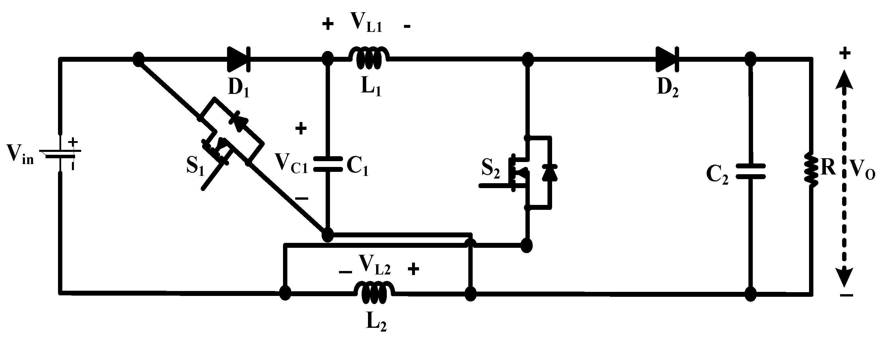
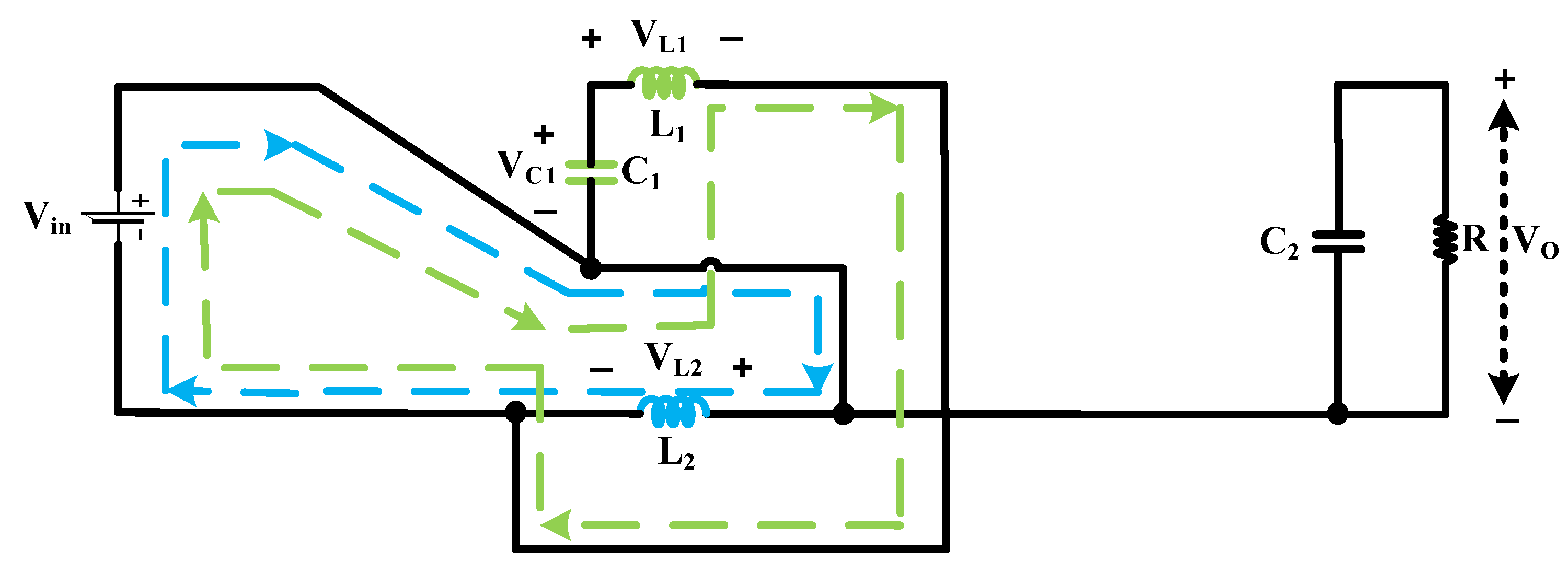
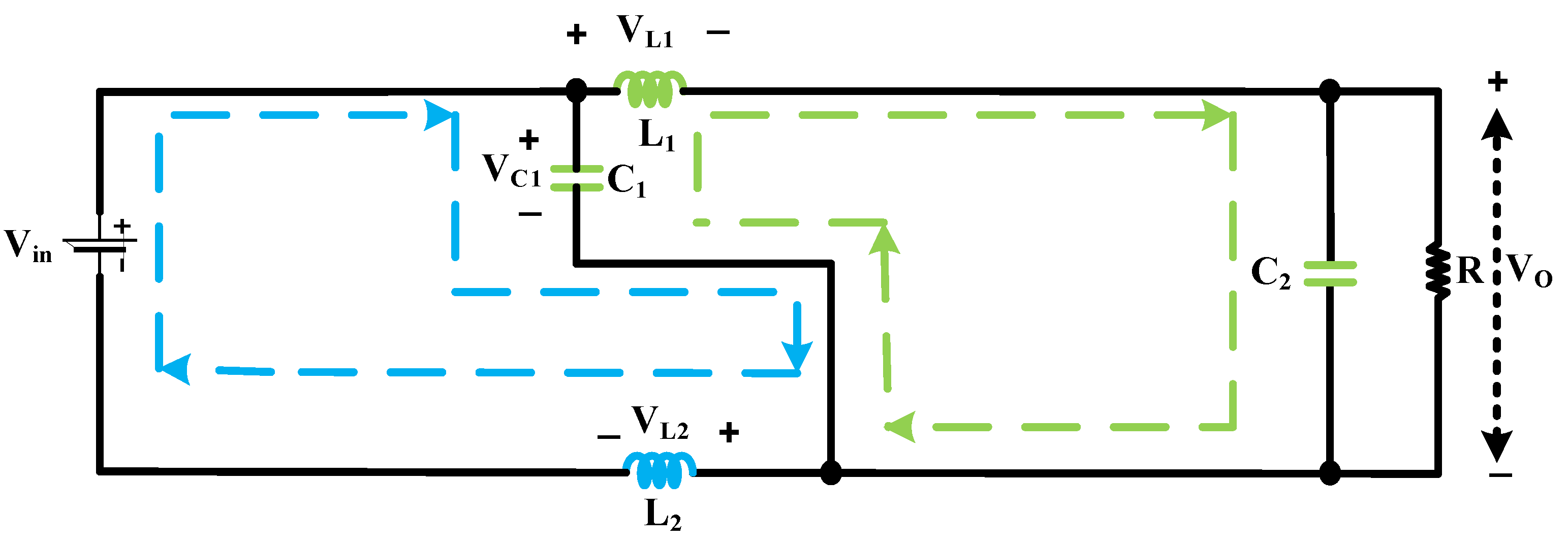
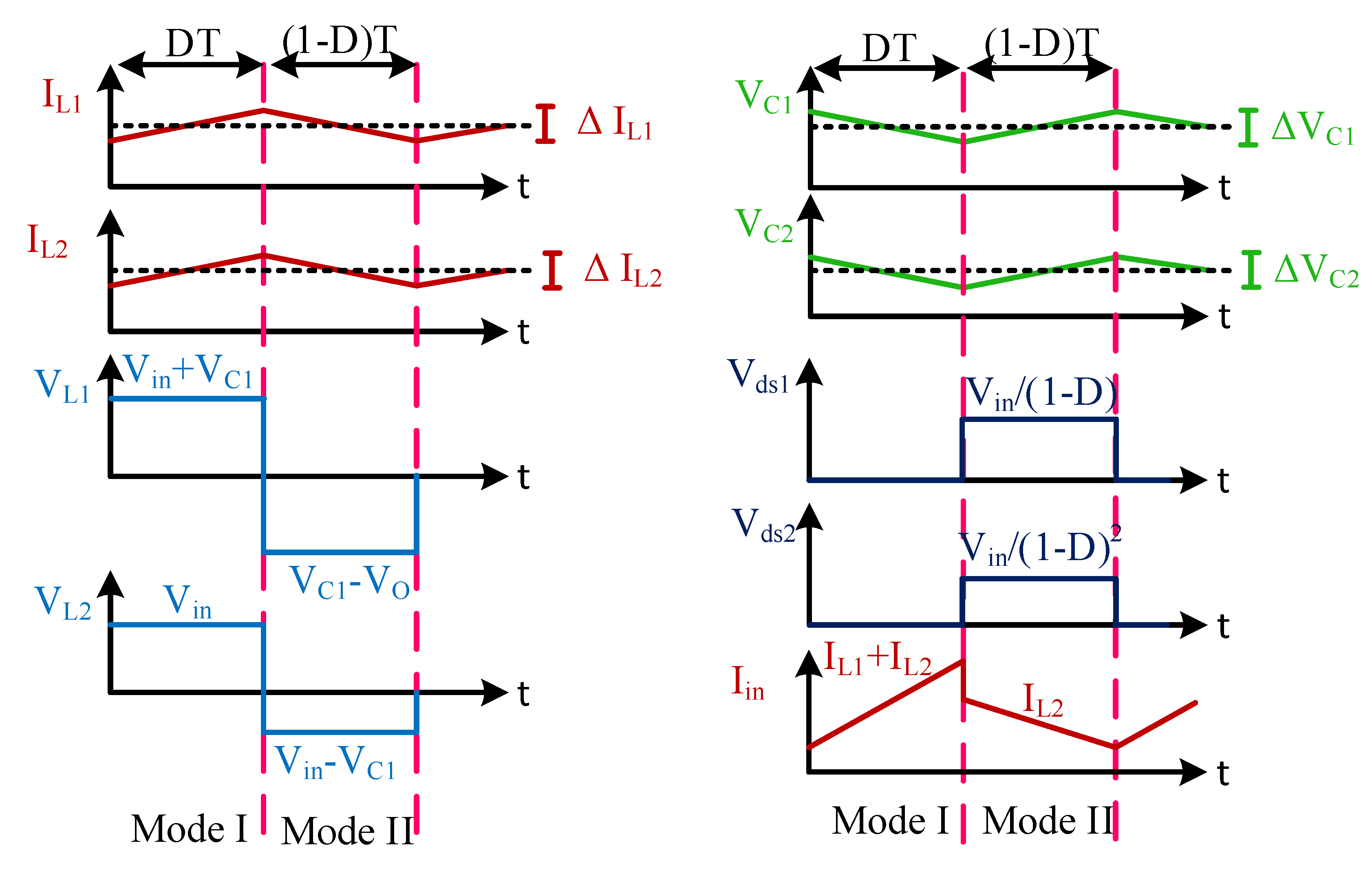
2. Structure and Working of the Proposed Converter

The circuit diagram of the proposed converter is shown in Figure 1. The control signal is the same for both the switches. Based on the control signal, there are two modes of operation; that is, switch-on mode of operation and switch-off mode of operation. The modes of operations can be explained as follows:
Mode 1: Both the switches are turned ON simultaneously, and hence diodes D1 and D2 are reverse-biased. The conduction diagram is given in Figure 2. In this operation mode, both the capacitors discharge and transfer their energy to the inductors and to the load, respectively, while both inductors store energy, and the inductor current subsequently increases linearly.
The governing equations for the first mode are as follows:
V L 1 = V i n + V C 1
V L 2 = V i n
Mode 2: The switches are turned OFF, and both the diodes conduct. Both the capacitors are charged during this mode of operation, while the energy of both the inductors is transferred to the load as their current decreases. The conduction diagram is shown in Figure 3. The equations for this mode are as shown below:
V L 1 = V C 1 V O
V L 2 = V i n V C 1
Applying the principle of volt-sec balance in inductor L2 and L1:
0 T V L 2 ( t ) · d t = 0
V i n × D T + ( V i n V C 1 ) × ( 1 D ) T = 0
V C 1 = V i n 1 D
0 T V L 1 ( t ) ·   d t = 0
( V i n + V C 1 ) × D T + ( V C 1 V O ) × ( 1 D ) T = 0
From Equations (7) and (9), the gain (M) is written as:
M = V o V i n = ( 1 + D D 2 ) ( 1 D ) 2
From Equation (10), it can be inferred that the voltage gain of the proposed converter is quadratic.

3. Design of Passive Components and Stress across Switches

3.1. Design of Inductors

Rewriting the equation of the first mode of operation in a differential form, we get:
L 1 d I L 1 d t = V i n + V C 1 ,     L 2 d I L 2 d t = V i n
Δ I L 1 = ( V i n + V C 1 ) D T L 1 ,     Δ I L 2 = V i n D T L 2
After combining Equations (7) and (12), we get:
Δ I L 1 = V i n ( 2 D ) D T ( 1 D ) L 1
The average current through L1 and L2 are:
I L 1 = V O R ( 1 D ) ,     I L 2 = V O ( 2 D D 2 ) R ( 1 D ) 2
The minimum current through the inductors are as follows:
( I L 1 ) M i n = V O R ( 1 D ) V i n ( 2 D ) D T 2 ( 1 D ) L 1
( I L 2 ) M i n = V O ( 2 D D 2 ) R ( 1 D ) 2 V i n D T L 2
For the continuous conduction operation mode, the minimum inductance required can be calculated as given:
L 1 ( 2 D ) D ( 1 D ) 2 R f s ( 1 + D D 2 )
L 2 D ( 1 D ) 4 R f s ( 1 + D D 2 )

3.2. Design of Capacitor

The selection of a capacitor depends on the minimum permissible ripple in the voltage across the capacitor. The charge stored by the capacitor is as follows:
Δ Q = C Δ V C
I C Δ T = C Δ V C
when the switch is ON, the current through each capacitor is as follows:
( I C 1 ) O N = V o R ( 1 D ) ,     ( I C 2 ) O N = V o R
After combining (20), (21), and (10), the value of capacitors can be calculated as follows:
C 1 = V i n ( 1 + D D 2 ) D R ( 1 D ) 3 Δ V C 1 f s
C 2 = V i n ( 1 + D D 2 ) D R ( 1 D ) 2 Δ V C 2 f s

3.3. Voltage Stress across Switches

The voltage stress across the various components is given by (24) and (25). It can be seen from (24) and (25) that stress across the switch S1 and S2 is less than VO.
V S 1 = V i n 1 D = V O ( 1 D ) ( 1 + D D 2 )
V S 2 = V i n ( 1 D ) 2 = V O ( 1 + D D 2 )
The related waveforms during continuous conduction mode are shown in Figure 4.

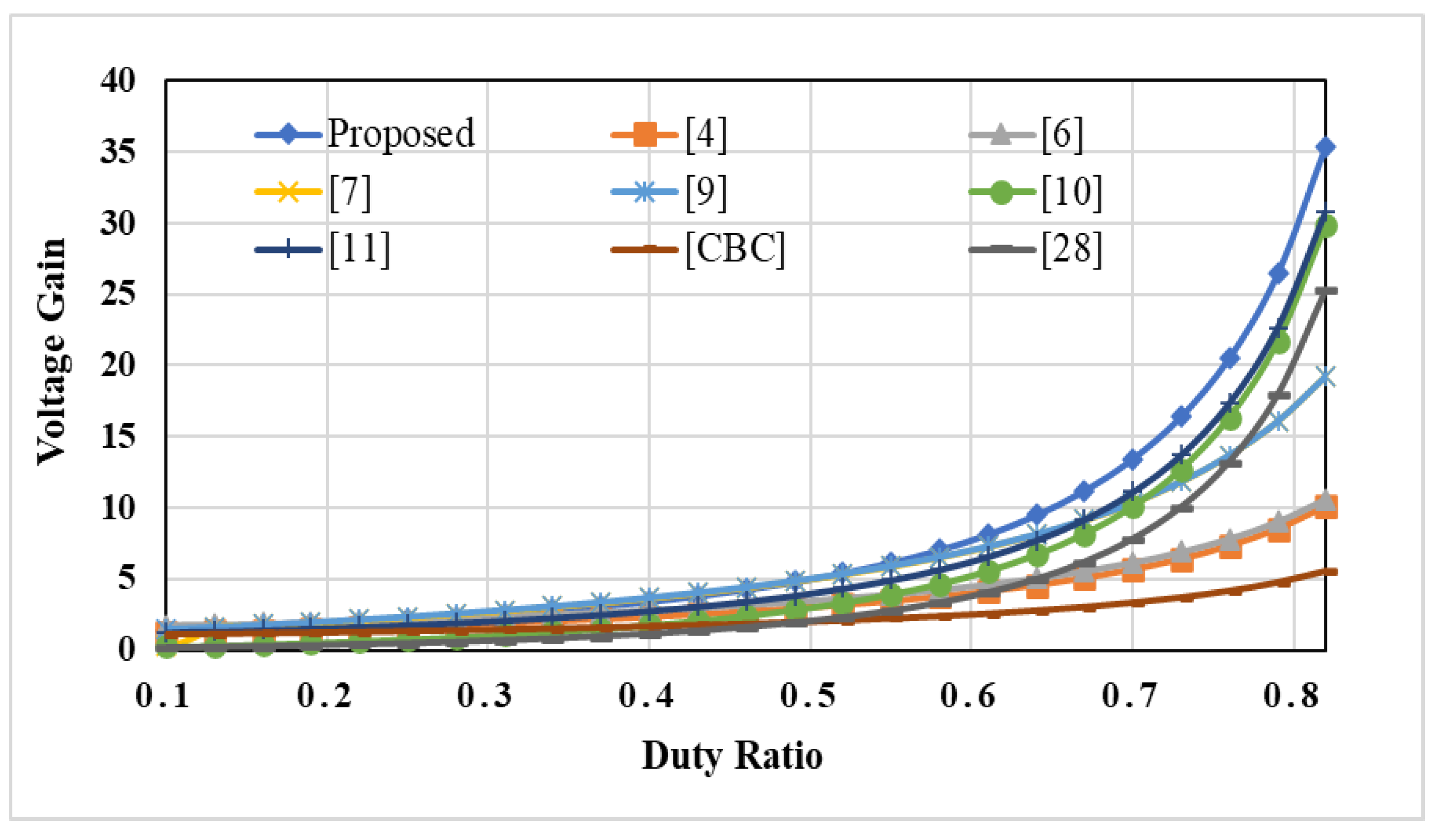
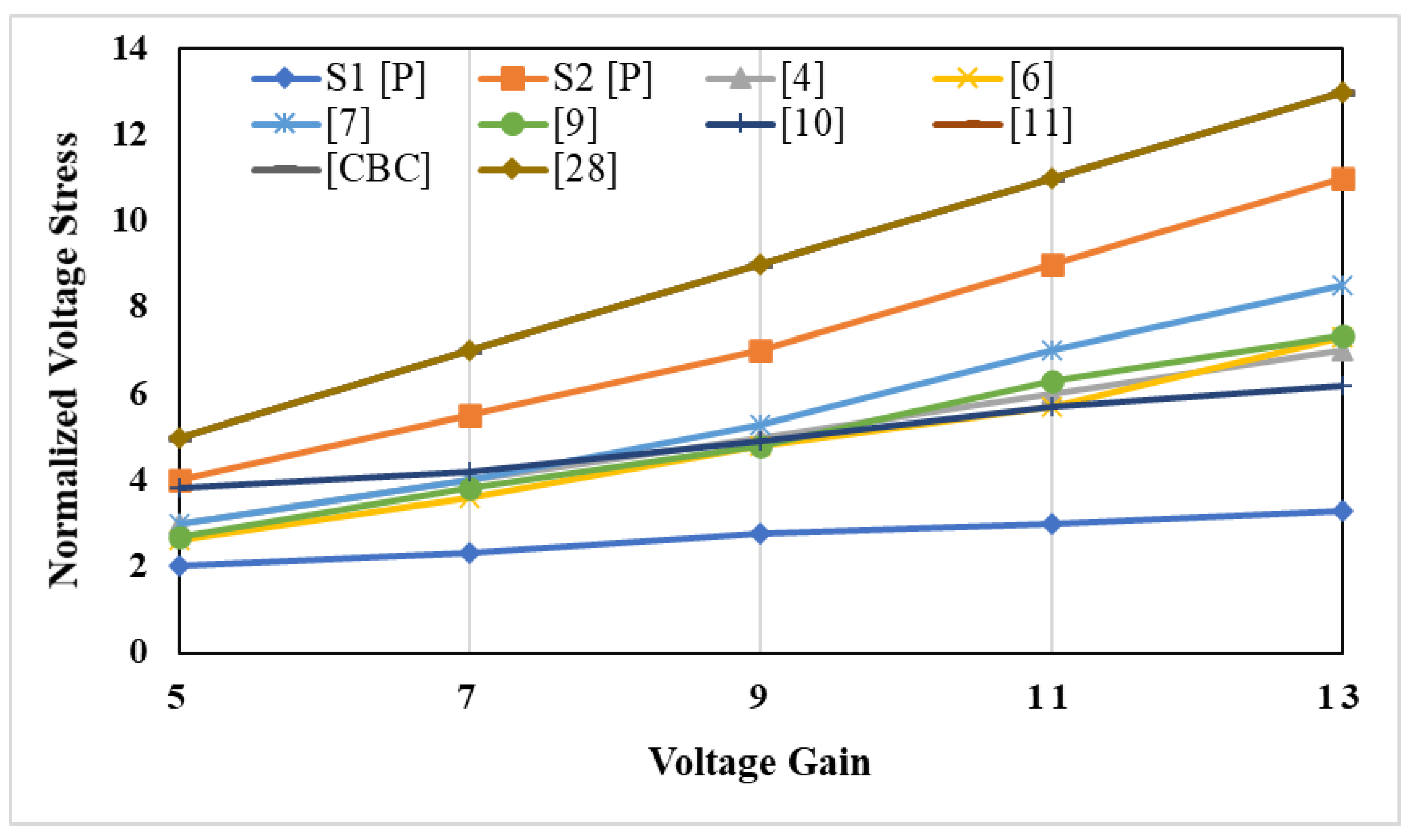
4. Comparison Assessment with Other Converters

In this section, the high-gain boost converter presented in this paper is compared. The comparison is shown in Table 1. The converter given in [4] had 2 inductors (L), 3 capacitors (C), and a single switch (S), but has lower gain than the presented converter. The converter given in [6] had a total number of 10 components with two inductors and 4 diodes, but its voltage gain was only 3.5 at a duty ratio of 0.5, whereas at D = 0.5, our proposed topology has a gain of 5.3. The modified buck-boost topology proposed in [7] had 4 inductors, 6 capacitors, and 3 diodes, but the substantial gain could be achieved only by operating it at high duty ratios. To obtain a gain of 15, the converter proposed in [7] needed to be run at 0.8 duty, whereas the converter presented here achieve a gain of more than 30 times at the same duty ratio. The switched inductor topology proposed in [9] employed a VMC made of diodes and an inductor for increasing the converter gain; 7 diodes and 4 inductors were utilized for increasing the converter gain, but the gain was still less than our proposed converter. The quadratic buck-boost converter proposed in [10] had the advantage of common ground, but the gain was not very high, and the input current was discontinuous, which made it unsuitable for solar PV applications. The conventional quadratic boost converter (CQBC) [11] also had two inductors, but its gain was low and the switch had voltage stress, which is equal to VO. Similarly, the converter proposed in [28] had three inductors and three capacitors; still, the gain was limited and stress across the switch was high. As can be observed in Figure 5, our proposed high-gain structure has a gain of 8 times at D = 0.6. The gain rapidly increases from 0.7 to 0.8 duty ratio. Apart from higher gain, the converter utilizes only 8 components, and hence losses in the ON state and parasitic resistance would be low. Figure 6 gives the normalized voltage stress across the switch of the converter. It can be observed that the two switches of the converter had different voltage stresses across them. As compared with other structures, the switch S1 had the lowest stress across it. The stress across switch S2 was less than VO but was higher than S1. Further, it can be observed that the stress across S2 also was less than in the converters proposed in [28] and the conventional quadratic boost converter (CQBC) proposed in [11].

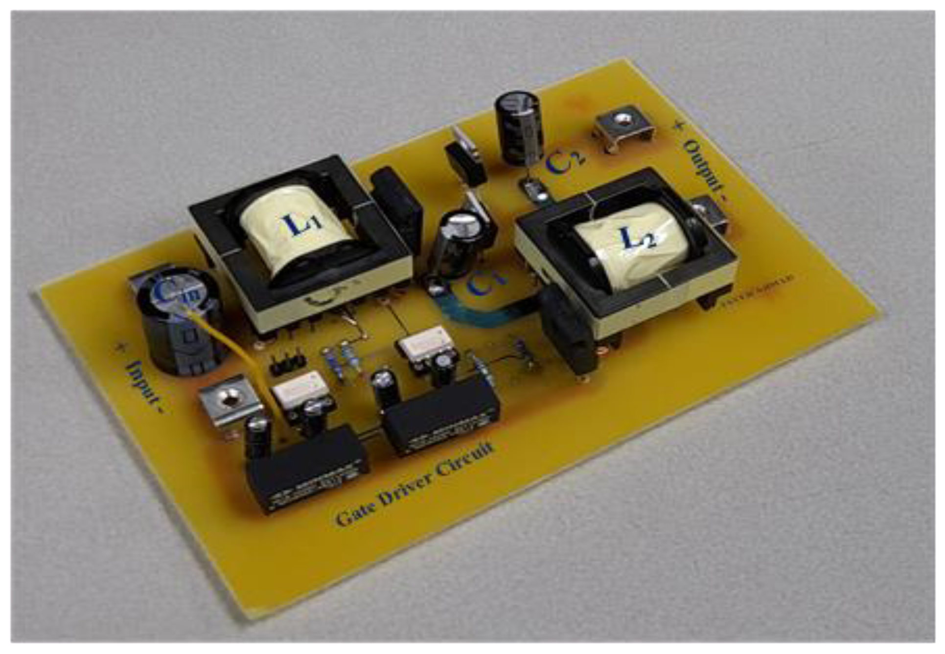
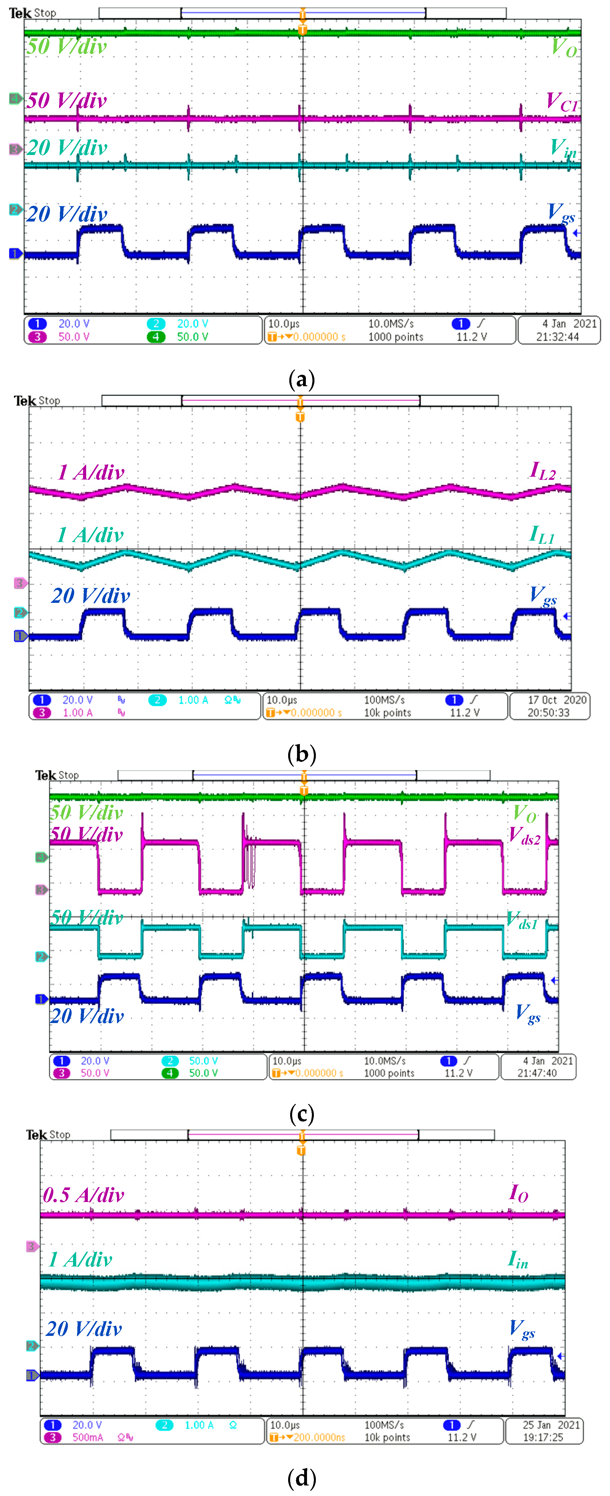
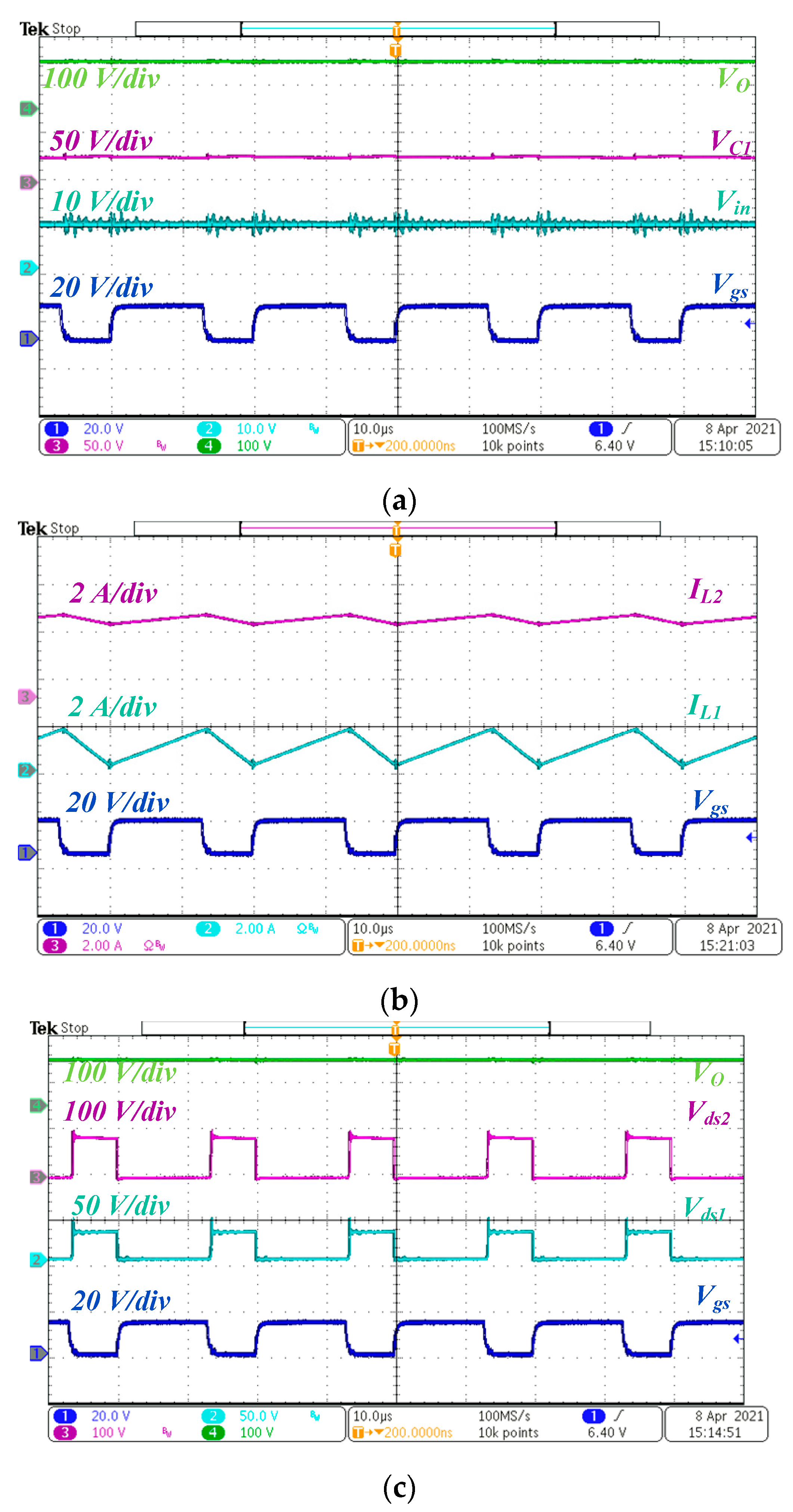
5. Experimental Results

Table 2 shows the specifications of the presented converter. The simulation results were validated by running it on a hardware prototype. The working of the converter was tested by building a 150 W prototype as given in Figure 7. The prototype was operated at a 0.4 duty ratio. From Figure 8a, the output voltage VO was equal to 80 V, which was proximate to the theoretical value. The voltage across the capacitor was found to be 40 V, which was half the VO. The converter was operating in continuous conduction mode, as evident from the waveforms of the inductor currents shown in Figure 8b. The voltage stress across switch S1 was found to be 40 V, and the stress across the switch S2 was found to be 65 V, as observed in Figure 8c. The stress across both switches was less than VO, which was an improvement over the other conventional topologies, thereby improving the efficiency. The converter had a continuous input current, which is its main advantage. The average input current Iin and output current IO were found to be 1.5 A and 0.4 A, respectively. Furthermore, the input current had a very low voltage ripple, which eliminated the need for any input filter.
Figure 9a shows the experimental results at a duty ratio of 0.65 and input voltage of 10 V, and it was found that the output voltage was almost 100 V, which also verified the calculated gain of 10 times. The voltage across the capacitor C1 was 27 V, which was almost the same as that of the calculated value. The inductor currents and voltage across switches are shown in Figure 9b,c.

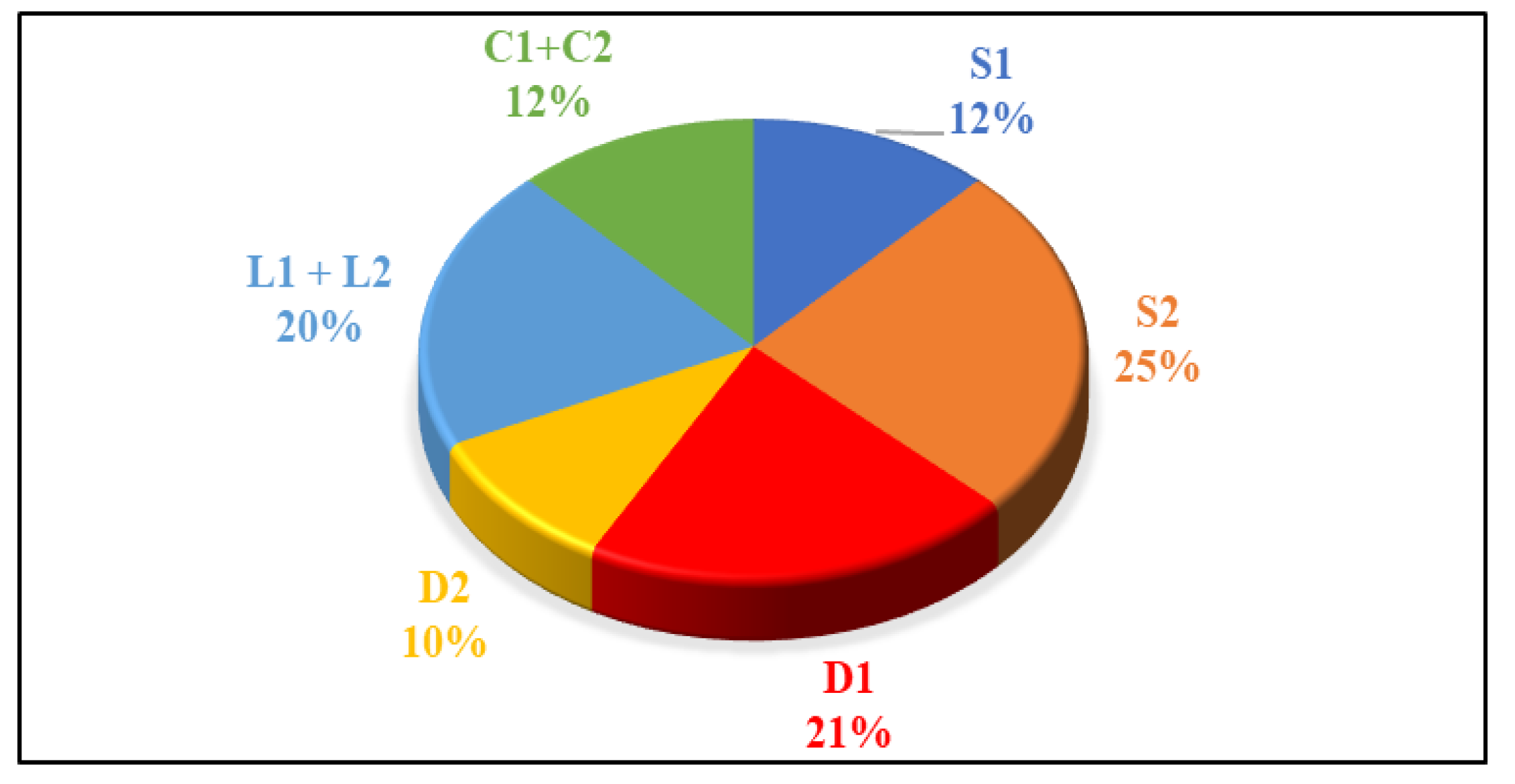
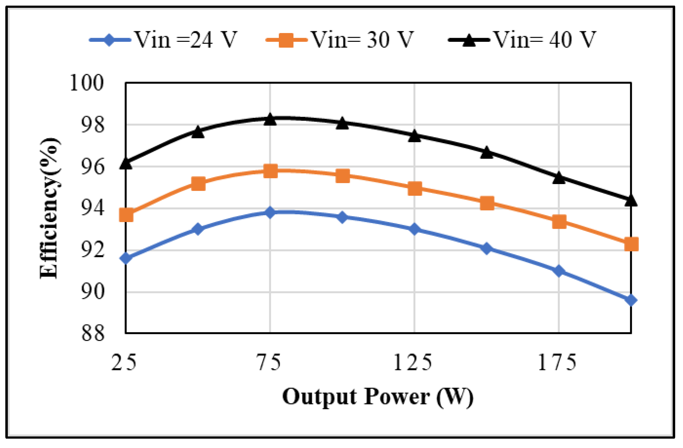
6. Efficiency Calculation

In this section, the power loss in different components of the converter is calculated. The power loss in the converter occurs because of parasitic resistances of inductor capacitors and ON-state resistance of switches and diodes.
Power loss in inductors: Neglecting the ripple in the current, the RMS and average current flowing in inductor can be assumed to be the same. The power loss due to parasitic resistance of inductors is as shown in (26):
P L 1 = V O 2 r L 1 R 2 ( 1 D ) 2 ,                 P L 2 = V O 2 ( 2 D D 2 ) 2 r L 2 R 2 ( 1 D ) 4
where r L 1 and r L 2 are parasitic resistances of inductors.
Power loss in capacitors: Similarly, the loss in capacitors due to ESR is as given below:
P C 1 = i C 1 R M S   2 r C 1 P C 1 = V O 2 D r C 1 R 2 ( 1 D ) 3
P C 2 = i C 2 R M S   2 r C 2 P C 2 = V O 2 D r C 2 R 2 ( 1 D )
Power loss in diodes: By knowing the RMS current, the average current of the total power loss across each diode is calculated as follows:
P D 1 = V D i D 1 a v g + i D 1 R M S   2 r D 1 P D 1 = V D V O R ( 1 D ) + V O 2 r D R 2 ( 1 D ) 4
P D 1 = V D i D 1 a v g + i D 1 R M S   2 r D 1 P D 2 = V D V O R ( 1 D ) + V O 2 r D R 2 ( 1 D )
where V D is the voltage drop across the diode.
Power loss in the switch: There are two types of switch losses: conduction loss ( P s w C o n d ) and switching loss ( P s w ) . These losses can be calculated as follows:
P s w = P s w C o n d + P s w O N + P s w O F F
P s w C o n d = I 2 s w R M S r s w O N
where r s w O N is ON-state resistance of MOSFET.
P s w 1 C o n d = V O 2 ( 2 D D 2 ) 2 R 2 ( 1 D ) 4 D r s w O N
P s w 2 C o n d = V O 2 R 2 ( 1 D ) 2 r s w O N
P s w O N = I s w O N V D D 2 × t r i + t f v 2 × f s
P s w 1 O N = V O ( 2 D D 2 ) V i n 2 R ( 1 D ) 3 × t r i + t f v 2 × f s
P s w 2 O N = V O V i n 2 R ( 1 D ) 3 × t r i + t f v 2 × f s
P s w 1 O F F = V O ( 2 D D 2 ) V i n 2 R ( 1 D ) 3 × t f i + t r v 2 × f s
P s w 2 O F F = V O V i n 2 R ( 1 D ) 3 × t f i + t r v 2 × f s
where: t r i + t f v 2 is turn ON time;
t f i + t r v 2 is turn OFF time; and
f s is switching frequency.
To find the actual output voltage equation, we can combine all the losses and apply the law of conservation of power. A simplified output voltage equation considering only inductor and capacitor losses is provided in (40):
V O = [ V i n ( 1 D ) ( 1 + D D 2 ) ] R ( 1 D ) R ( 1 D ) 4 + r L 1 ( 1 D ) 2 + r L 2 ( 4 D 2 + D 2 4 D 3 ) + r C 1 D ( 1 D ) + r C 2 D ( 1 D ) 3
Equation (40) can be verified by using the values of parameters from Table 2. The value of VO is found to be 82.1 V for Vin = 24 V and D = 0.4, which is very close to the experimental value of 80 V.
V O = [ 24 ( 1 0.4 ) ( 1 + 0.4 0.4 2 ) ] ( 300 ) ( 1 0.4 ) 39 + 0.072 + 0.0272 + 0.036 + 0.013 = 82.1   V
The bifurcation of losses in converter is shown in Figure 10. The total losses in the MOSFETs accounted for 40% of the total losses. The total losses in diodes were 31%. In Figure 11, efficiency of converter is plotted at different values of input voltages. At low input voltages, the peak efficiency was found to be low. This is because high current flows in the circuit for achieving the same output power, and hence more losses occurred in the converter. The converter efficiency was high if the input voltages were between 24 and 40 V. Usually, the output from the solar PV module is 24 V. Hence, the proposed converter may be applied for stepping-up the voltage with high efficiency in the power range of 200–300 W.

7. Conclusions

A new high-gain converter was proposed and analyzed. The proposed converter utilized only a total of eight components to achieve high quadratic voltage gain. Usually, converters that produce quadratic voltage gain utilize more than three inductors and several diodes. The converter has a continuous input current, which is its main feature as it increases the life of solar PV panels. A hardware prototype of 150 W was developed in laboratory. Experimental results validated the workings and performance of converter. The converter was superior to quadratic boost, conventional boost, and other high-gain converters in terms of gain and voltage stress across switch. The peak efficiency of the converter was found to be 93.7% for Vin = 24 V. The merits of converter make it worthy for renewable energy applications for an output power in the range of 200–300 W.

Author Contributions

All authors contributed equally in the preparation and revision of the manuscript. All authors have read and agreed to the published version of the manuscript.

Funding

The authors would like to acknowledge financial support from the Taif University Researchers Supporting Project (Number TURSP-2020/278), Taif University, Taif, Saudi Arabia. The authors also acknowledge the support provided by the Hardware-In-the-Loop (HIL) Lab and Non-Conventional Energy (NCE) Lab., Department of Electrical Engineering, Aligarh Muslim University, India.

Institutional Review Board Statement

Not Applicable.

Informed Consent Statement

Not Applicable.

Data Availability Statement

Not Applicable.

Conflicts of Interest

The authors declare no conflict of interest.

References

  1. Forouzesh, M.; Siwakoti, Y.P.; Gorji, S.A.; Blaabjerg, F.; Lehman, B. Step-Up DC–DC Converters: A Comprehensive Review of Voltage-Boosting Techniques, Topologies, and Applications. IEEE Trans. Power Electron. 2017, 32, 9143–9178. [Google Scholar] [CrossRef]
  2. Tofoli, F.L.; Pereira, D.D.C.; de Paula, W.J.; Júnior, D.D.S.O. Survey on non-isolated high-voltage step-up dc–dc topologies based on the boost converter. IET Power Electron. 2015, 8, 2044–2057. [Google Scholar] [CrossRef] [Green Version]
  3. Cornea, O.; Andreescu, G.-D.; Muntean, N.; Hulea, D. Bidirectional Power Flow Control in a DC Microgrid Through a Switched-Capacitor Cell Hybrid DC–DC Converter. IEEE Trans. Ind. Electron. 2017, 64, 3012–3022. [Google Scholar] [CrossRef]
  4. Shahir, F.M.; Babaei, E.; Farsadi, M. Voltage-Lift Technique Based Nonisolated Boost DC–DC Converter: Analysis and Design. IEEE Trans. Power Electron. 2017, 33, 5917–5926. [Google Scholar] [CrossRef]
  5. Padmanaban, S.; Bhaskar, M.S.; Maroti, P.K.; Blaabjerg, F.; Fedák, V. An original transformer and switched capacitor (T & SC)- based extension for DC-DC boost converter for high-voltage/low- current renewable energy applica-tions: Hardware implementation of a new T & SC boost converter. Energies 2018, 11, 783. [Google Scholar] [CrossRef] [Green Version]
  6. Saravanan, S.; Babu, N.R. Design and Development of Single Switch High Step-Up DC–DC Converter. IEEE J. Emerg. Sel. Top. Power Electron. 2017, 6, 855–863. [Google Scholar] [CrossRef]
  7. Banaei, M.R.; Sani, S.G. Analysis and Implementation of a New SEPIC-Based Single-Switch Buck–Boost DC–DC Converter With Continuous Input Current. IEEE Trans. Power Electron. 2018, 33, 10317–10325. [Google Scholar] [CrossRef]
  8. Shanthi, T.; Prabha, S.U.; Sundaramoorthy, K. Non-isolated n-stage High Step-up DC-DC Converter for Low voltage DC Source Integration. IEEE Trans. Energy Convers. 2021. [Google Scholar] [CrossRef]
  9. Wu, B.; Li, S.; Liu, Y.; Smedley, K.M. A New Hybrid Boosting Converter for Renewable Energy Applications. IEEE Trans. Power Electron. 2016, 31, 1203–1215. [Google Scholar] [CrossRef]
  10. Gorji, S.A.; Mostaan, A.; My, H.T.; Ektesabi, M. Non-isolated buck–boost dc–dc converter with quadratic voltage gain ratio. IET Power Electron. 2019, 12, 1425–1433. [Google Scholar] [CrossRef]
  11. Diaz-Saldierna, L.; Morales-Saldaña, J.; Ortiz-Lopez, M. Switching regulator using a quadratic boost converter for wide DC conversion ratios. IET Power Electron. 2009, 2, 605–613. [Google Scholar] [CrossRef]
  12. Starzyk, J.A.; Jan, Y.-W.; Qiu, F. A DC-DC charge pump design based on voltage doublers. IEEE Trans. Circ. Syst. I Regul. Pap. 2001, 48, 350–359. [Google Scholar] [CrossRef] [Green Version]
  13. Luo, F.L.; Ye, H. Positive output multiple-lift push–pull switched capacitor Luo-converters. IEEE Trans. Ind. Electron. 2004, 51, 594–602. [Google Scholar] [CrossRef]
  14. Lee, S.-W.; Do, H.-L. Quadratic Boost DC–DC Converter With High Voltage Gain and Reduced Voltage Stresses. IEEE Trans. Power Electron. 2018, 34, 2397–2404. [Google Scholar] [CrossRef]
  15. Wai, R.-J.; Lin, C.-Y.; Duan, R.-Y. High-efficiency DC-DC converter with high voltage gain and reduced switch stress. IEEE Trans. Ind. Electron. 2007, 54, 354–364. [Google Scholar] [CrossRef]
  16. Lee, J.; Liang, T.; Chen, J. Isolated coupled-inductor-integrated DC-DC converter with non-dissipative snubber for solar energy applications. IEEE Trans. Ind. Electron. 2014, 61, 3337–3348. [Google Scholar] [CrossRef]
  17. Azizkandi, M.E.; Sedaghati, F.; Shayeghi, H.; Blaabjerg, F. A High Voltage Gain DC–DC Converter Based on Three Winding Coupled Inductor and Voltage Multiplier Cell. IEEE Trans. Power Electron. 2019, 35, 4558–4567. [Google Scholar] [CrossRef]
  18. Duong, T.-D.; Nguyen, M.-K.; Tran, T.-T.; Lim, Y.-C.; Choi, J.-H. Transformerless High Step-Up DC-DC Converters with Switched-Capacitor Network. Electronics 2019, 8, 1420. [Google Scholar] [CrossRef] [Green Version]
  19. Ahmad, J.; Zaid, M.; Sarwar, A.; Tariq, M.; Sarwer, Z. A New Transformerless Quadratic Boost Converter with High Voltage Gain. Smart Sci. 2020, 8, 1–21. [Google Scholar] [CrossRef]
  20. Park, K.B.; Moon, G.W.; Youn, A.J. Non isolated high step-up boost converter integrated with sepic converter. IEEE Trans. Power Electron. 2010, 25, 2266–2275. [Google Scholar] [CrossRef]
  21. Meraj, M.; Bhaskar, M.S.; Iqbal, A.; Al-Emadi, N.; Rahman, S. Interleaved Multilevel Boost Converter With Minimal Voltage Multiplier Components for High-Voltage Step-Up Applications. IEEE Trans. Power Electron. 2020, 35, 12816–12833. [Google Scholar] [CrossRef]
  22. Zhu, B.; Chen, S.; Zhang, Y.; Huang, Y. An Interleaved Zero-Voltage Zero-Current Switching High Step-Up DC-DC Converter. IEEE Access 2021, 9, 5563–5572. [Google Scholar] [CrossRef]
  23. Alzahrani, A.; Ferdowsi, M.; Shamsi, P. A Family of Scalable Non-Isolated Interleaved DC-DC Boost Converters with Voltage Multiplier Cells. IEEE Access 2019, 7, 11707–11721. [Google Scholar] [CrossRef]
  24. Dwari, S.; Parsa, L. An Efficient High-Step-Up Interleaved DC–DC Converter with a Common Active Clamp. IEEE Trans. Power Electron. 2010, 26, 66–78. [Google Scholar] [CrossRef]
  25. Deng, J.; Wang, H.; Shang, M. A ZVS Three-Port DC/DC Converter for High-Voltage Bus-Based Photovoltaic Systems. IEEE Trans. Power Electron. 2019, 34, 10688–10699. [Google Scholar] [CrossRef]
  26. Babaei, E.; Maheri, H.M.; Sabahi, M.; Hosseini, S.H. Extendable Non-isolated High Gain DC-DC Converter Based on Active–Passive Inductor Cells. IEEE Trans. Ind. Electron. 2018, 65, 9478–9487. [Google Scholar] [CrossRef]
  27. Lakshmi, M.; Hemamalini, S. Non-isolated High Gain DC–DC Converter for DC Microgrids. IEEE Trans. Ind. Electron. 2018, 65, 1205–1212. [Google Scholar] [CrossRef]
  28. Iqbal, A.; Member, S. A New Structure of High Voltage Gain SEPIC Converter for Renewable Energy Applications. IEEE Access 2019, 7, 89857–89868. [Google Scholar]
  29. Rosas-Caro, C.J.; Mancilla-David, F.; Mayo-Maldonado, J.C.; Gonzalez-Lopez, J.M.; Torres-Espinosa, H.L.; Valdez-Resendiz, J.E. A Transformer-less High-Gain Boost Converter with Input Current Ripple Cancelation at a Selectable Duty Cycle. IEEE Trans. Ind. Electron. 2013, 60, 4492–4499. [Google Scholar] [CrossRef]
  30. Guepfrih, M.F.; Waltrich, G.; Lazzarin, T.B. High Step-Up Dc-Dc Converter Using Built-in Transformer Voltage Multiplier Cell and Dual Boost Concepts. IEEE J. Emerg. Sel. Top. Power Electron. 2021. [Google Scholar] [CrossRef]
  31. Andrade, A.M.S.S.; Faistel, T.; Guisso, R.A.; Toebe, A. Hybrid High Voltage Gain Transformerless DC-DC Converter. IEEE Trans. Ind. Electron. 2021. [Google Scholar] [CrossRef]
  32. Mahmood, A.; Zaid, M.; Ahmad, J.; Khan, M.A.; Khan, S.; Sifat, Z.; Lin, C.-H.; Sarwar, A.; Tariq, M.; Alamri, B. A Non-inverting High Gain DC-DC Converter with Continuous Input Current. IEEE Access 2021, 9, 54710–54721. [Google Scholar] [CrossRef]
  33. Khan, S.; Mahmood, A.; Tariq, M.; Zaid, M.; Khan, I.; Rahman, S. Improved Dual Switch Non-Isolated High Gain Boost Converter for DC microgrid Application. In Proceedings of the 2021 IEEE Texas Power and Energy Conference (TPEC), College Station, TX, USA, 2–5 February 2021; pp. 1–6. [Google Scholar] [CrossRef]
  34. Khan, S.; Zaid, M.; Mahmood, A.; Ahmad, J.; Alam, A. A Single Switch High Gain DC-DC converter with Reduced Voltage Stress. In Proceedings of the 2020 IEEE 7th Uttar Pradesh Section International Conference on Electrical, Electronics and Computer Engineering (UPCON), Prayagraj, India, 27–29 November 2020; pp. 1–6. [Google Scholar]
  35. Zaid, M.; Ahmad, J.; Sarwar, A.; Sarwer, Z.; Tariq, M.; Alam, A. A Transformerless Quadratic Boost High Gain DC-DC Converter. In Proceedings of the 2020 IEEE International Conference on Power Electronics, Drives and Energy Systems (PEDES), Jaipur, India, 16–19 December 2020; pp. 1–6. [Google Scholar]
Figure 1. The proposed converter.
Energies 14 02629 g001
Figure 2. Conduction diagram for the first mode of operation.
Energies 14 02629 g002
Figure 3. Conduction diagram for the second mode of operation.
Energies 14 02629 g003
Figure 4. Related waveforms in CCM.
Energies 14 02629 g004
Figure 5. Comparision of the Voltage gain for different converters.
Energies 14 02629 g005
Figure 6. Comparison of stress across the switches.
Energies 14 02629 g006
Figure 7. Prototype of the proposed converter.
Energies 14 02629 g007
Figure 8. Experimental results at Vin = 24 V, D = 0.4. (a) VO, VC1, and Vin. (b) IL1 and IL2. (c) VO, Vds1, and Vds2. (d) Io, Iin, and Vgs.
Energies 14 02629 g008
Figure 9. Experimental results at Vin = 10 V, D = 0.65. (a) VO, VC1, and Vin. (b) IL1 and IL2. (c) VO, Vds1, Vds2.
Energies 14 02629 g009
Figure 10. The breakup of losses of the proposed converter at 25 W output.
Energies 14 02629 g010
Figure 11. Efficiency of converter at different input voltages.
Energies 14 02629 g011
Table 1. Comparison of the proposed converter with similar topologies.
TopologyInductorsCapacitorsSwitchesDiodesTotal ComponentsVoltage Gain
( V o / V i n )
Normalized Voltage Stress
( V S / V i n )
[4]23139 1 + D ( 1 D ) 1 1 D
[6]231410 3 + D 2 ( 1 D ) 1 1 D
[7]461314 3 D ( 1 D ) 1 1 D
[9]412714 1 + 3 D ( 1 D ) 1 + D 1 D
[10]22138 D ( 2 D ) ( 1 D ) 2 2 ( 1 D )
[11]22138 1 ( 1 D ) 2 1 ( 1 D ) 2
[28]33139 D ( 1 D ) 2 D ( 1 D ) 2
Proposed22228 1 + D D 2 ( 1 D ) 2 S 1 [ P ] = 1 1 D
S 2 [ P ] = 1 ( 1 D ) 2
Table 2. Ratings of components.
ElementsRating/Model
Vin24 V, 10 V
Po (max)150 W
fs50 kHz
R (Load)250 Ω, 300 Ω
InductorsL1 = L2 = 330 µH, ESR = 0.2 Ω
CapacitorsC1 = C2 = 33 µF 200 V, ESR = 0.15 Ω
S1 and S2SPW52N50C3
D1 and D2SF8L60USM
Gate Drivers ICTLP250H
MicrocontrollerSTM32 Nucleo H743ZI2
Publisher’s Note: MDPI stays neutral with regard to jurisdictional claims in published maps and institutional affiliations.

