Article

Software-Based Wireless Power Transfer Platform for Various Power Control Experiments

1
Institute for Information & communications Technology Promotion (IITP), Daejeon 305-348, Korea
2
School of Electrical Engineering, Korea University, Seoul 136-713, Korea
3
Department of Electrical Engineering, Kookmin University, Seoul 136-702, Korea
*
Author to whom correspondence should be addressed.
Energies 2015, 8(8), 7677-7689; https://doi.org/10.3390/en8087677
Submission received: 19 May 2015 / Revised: 29 June 2015 / Accepted: 20 July 2015 / Published: 28 July 2015
(This article belongs to the Special Issue Wireless Power Transfer)

Abstract

:
In this paper, we present the design and evaluation of a software-based wireless power transfer platform that enables the development of a prototype involving various open- and closed-loop power control functions. Our platform is based on a loosely coupled planar wireless power transfer circuit that uses a class-E power amplifier. In conjunction with this circuit, we implement flexible control functions using a National Instruments Data Acquisition (NI DAQ) board and algorithms in the MATLAB/Simulink. To verify the effectiveness of our platform, we conduct two types of power-control experiments: a no-load or metal detection using open-loop power control, and an output voltage regulation for different receiver positions using closed-loop power control. The use of the MATLAB/Simulink software as a part of the planar wireless power transfer platform for power control experiments is shown to serve as a useful and inexpensive alternative to conventional hardware-based platforms.

Graphical Abstract

1. Introduction

In recent years, planar wireless power transfer has attracted significant attention [1,2,3]. In particular, the widespread usage of mobile devices such as smart phones and tablet computers has led to the need for planar wireless power transfer. Recently, several standards organizations such as the Wireless Power Consortium (WPC), the Alliance for Wireless Power (A4WP), and the Power Matters Alliance (PMA) have been developing de facto standards for smartphone wireless charging. For example, WPC released the Qi standard in 2011 [4]. Also, there are various research results about applying wireless power transfer to traditional communication [5]. For example, in [6], the combination of information transfer and power transfer was proposed.
One of the important issues to be addressed in the design of various planar wireless power transfer systems is the occurrence of power fluctuation, which is caused by coupling and loading variations. Because of these power fluctuations, excessive power could be transmitted to accommodate all receivers’ charging conditions, substantially reducing the overall power efficiency, while imposing potential safety concerns. Power control in the field of wireless power transfer can be realized using two different methods: open- and closed-loop power controls. First, wireless power transfer systems should address several safety issues by employing an open-loop power control. For example, a wireless power transfer system should not turn on its transmitter when no load exists. Further, it should not heat up metal objects placed on or near the charging surface [7]. Next, it is necessary to stabilize the received power over a wide range of coupling and loading variations using the open- and closed-loop power control [8,9,10]. In general, the closed-loop power control monitors power-level variations in the receiver and transmits this data to the transmitter controller via a communication link. After receiving the power-level data, the controller can vary the supply voltage of the power amplifier [11,12] or change the resonant capacitor value to detune the transmitter coil [13]. The transmitter should change its transmitted power such that the received power remains slightly above the minimum level to maintain the receiver operation [14].
To date, there have been various studies on the implementation of power control functions for wireless power transfer. For example, in [15], authors developed a power control scheme using only analog feedback circuits. In [11,12], a custom application-specific integrated circuit (ASIC) was developed for wireless power transfer. In [7,8,9,10], a commercial microcontroller-based power control method was proposed. In [14,16], closed-loop power control was implemented using a commercial off-the-shelf (COTS) chipset. However, the implementation and verification of their power control functions are slightly time consuming, mainly because the development of new hardware for the real-time evaluation of a new power control requires much effort [17]. For example, software algorithms should be implemented on newly developed hardware using a microcontroller-dependent programming language or a hardware description language such as Verilog [18]. Fortunately, recent performance improvements of personal computers (PCs) and commercial simulation software have led to the development of software-based platforms that are capable of executing various algorithms, mostly under real-time conditions [19]. In this paper, we present the design and evaluation of a software-based wireless power transfer platform that allows us to perform flexible open- and closed-loop power control experiments. The proposed platform is based on a loosely coupled planar wireless power transfer circuit that uses a class-E power amplifier. The underlying power control function is implemented using an NI DAQ (National Instruments Data Acquisition) and algorithms in the MATLAB/Simulink software package. As opposed to the conventional hardware-based platform, implementation with MATLAB/Simulink software facilitates the modification of power control algorithms, avoiding a long and costly process for the development of separate control hardware. In fact, the use of MATLAB/Simulink software as a part of the planar wireless power transfer system for power control experiments serves as a useful and inexpensive alternative to the conventional hardware-based platform.

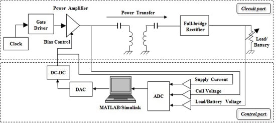
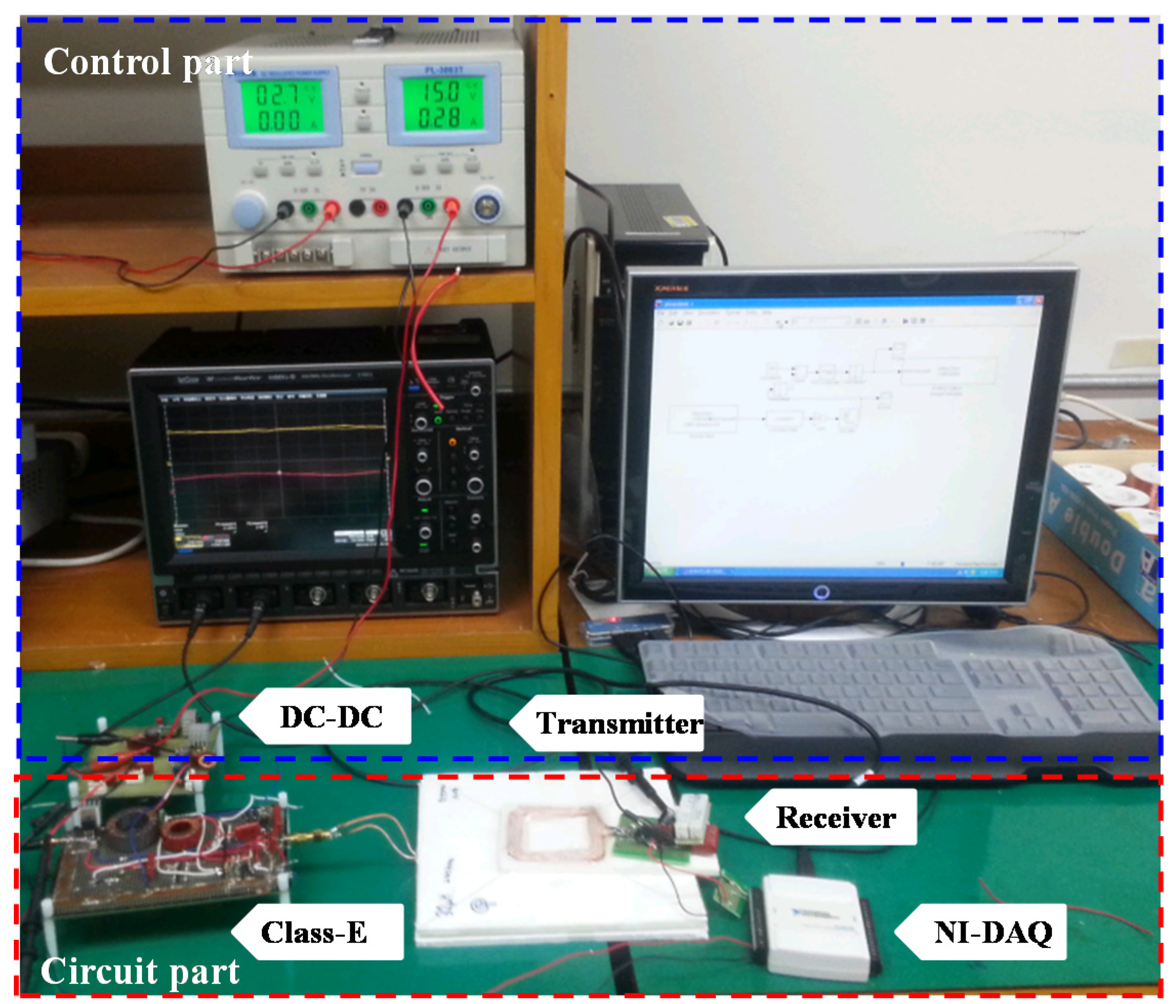
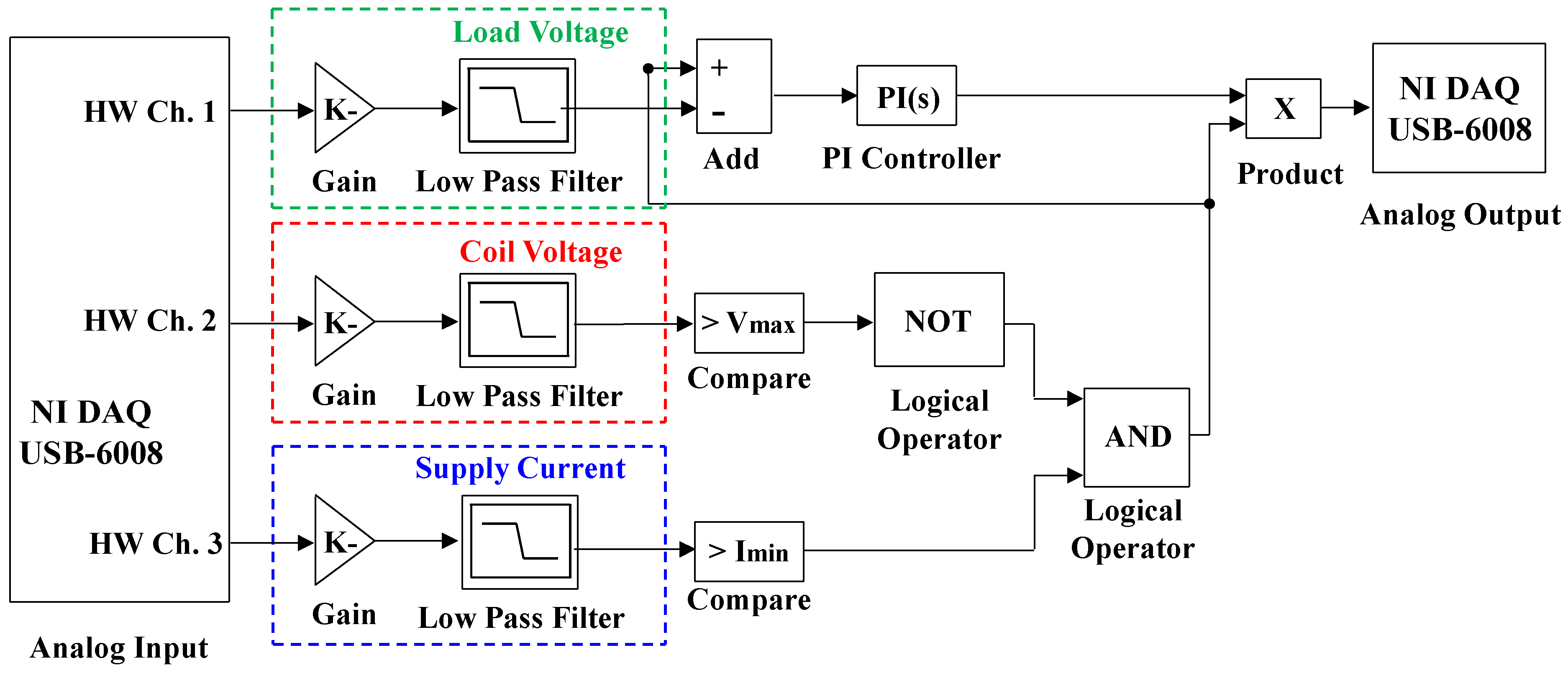
2. Proposed System Architecture

The block diagram in Figure 1 illustrates the proposed software-based wireless power transfer platform for various power control experiments. The proposed platform is divided into two different parts. The upper circuit part is a loosely coupled planar wireless power transfer circuit constructed using the class-E power amplifier via inductive coupling. First, the class-E switching-mode power amplifier is followed by a transmitter coil. The class-E amplifier is selected over the popular class-D amplifier due to its simplicity and high efficiency operation [20]. However, the class-D amplifier also can be used in our platform and there is no limitation on the selection of another type of power amplifier. The transmitter coil is in turn inductively coupled to the receiver coil. Finally, a full bridge rectifier is adopted to convert AC power to DC. The lower control part consists of a PC, an NI DAQ-6008 Digital-to-Analog Converter/Analog-to-Digital Converter (DAC/ADC) board, a designed DC–DC buck converter, and control programs that are implemented in MATLAB/Simulink. To monitor the transmitter and receiver status, the control part uses three sensors. With this sensing information, the power control algorithm controls the class-E power amplifier through a DC–DC converter via the DAC of the NI DAQ-6008 board.
Figure 1. Overall block diagram of software-based wireless power transfer platform for power control experiments.
Energies 08 07677 g001

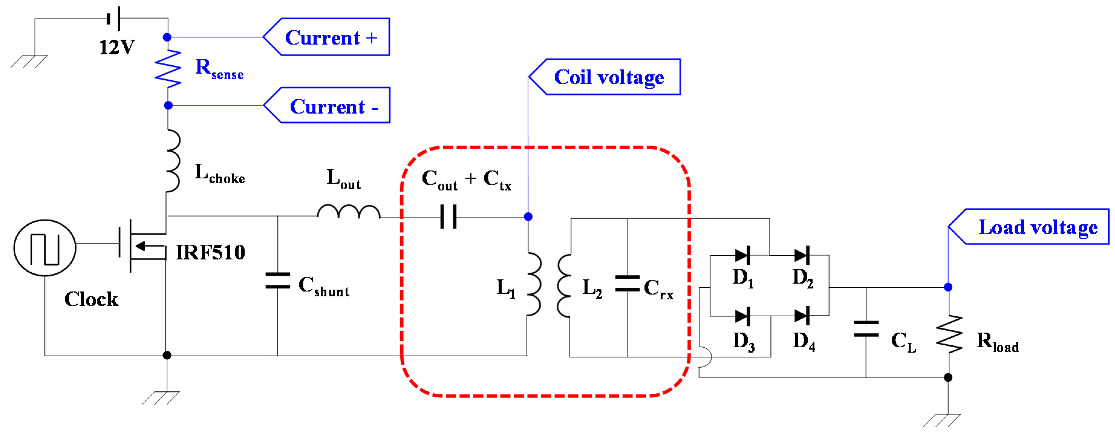
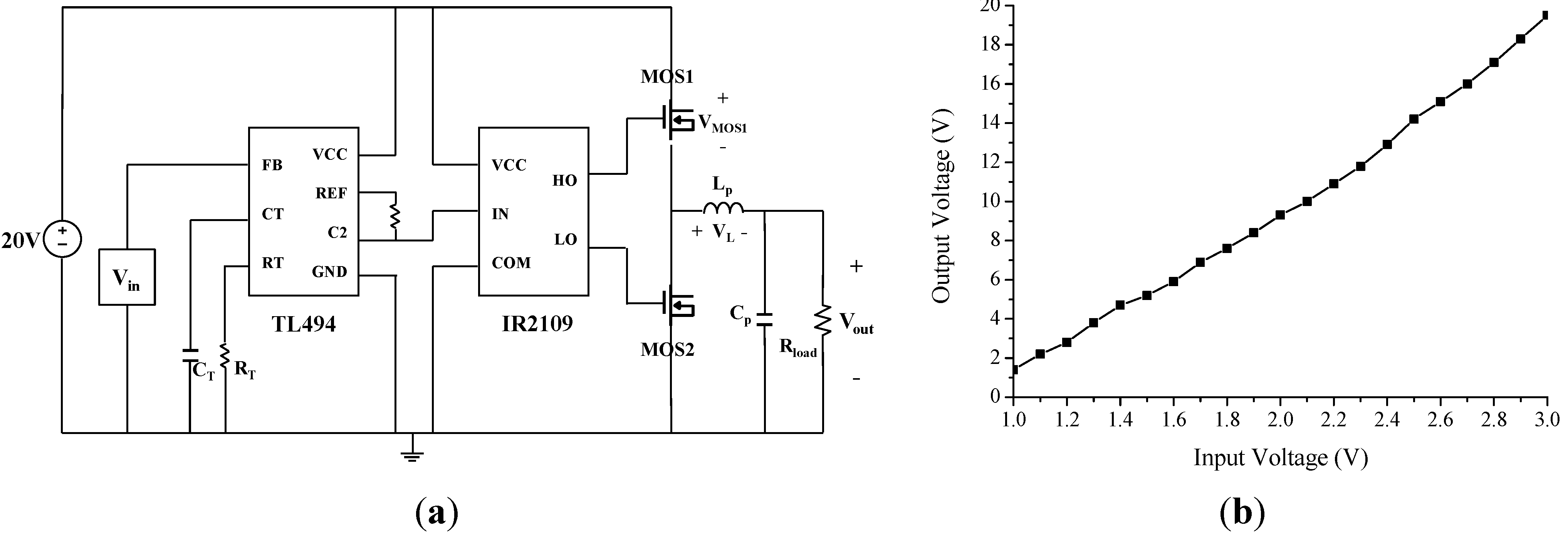
2.1. Circuit Part Design

Figure 2 shows a schematic of the fabricated wireless power transfer circuit, which mainly consists of a class-E power amplifier, a transmitter and receiver coil pair, and a full bridge rectifier implemented using Schottky diodes. The inverter is a class-E power amplifier that uses an inexpensive IRF510 power MOSFET (International Rectifier Co. Ltd., El Segundo, CA, USA) driven by a low-power clock at 240 kHz. The class-E power amplifier drives the transmitter coil L1. The induced voltage at L2 is amplified by the resonant tank L2-Crx. Rectification is achieved via four Schottky diodes and a charging storage capacitor CL. To achieve the optimum performance, component values of Lchoke, Cshunt, Lout, Cout, Ctx, and Crx are selected using the general design rules presented in [21]. In a coil pair, we used an impedance transformation network as shown in the red dotted box in Figure 2. The purpose of impedance transformation networks on the primary and secondary sides of the coupling is to achieve maximum power transfer and maximum efficiency by operating within the optimum impedance range [21]. From the four well-known topologies of impedance transformation networks [20], we chose the series-parallel topology such as the red-dotted box in Figure 2, because the series topology of the transmitter coil can share the output series capacitor of the class-E power amplifier while the parallel topology of the receiver part can alleviate the load variations of the receiver. The transmitter and receiver coils are constructed by hand using 100-strand #40 Litz wire to reduce the resistive losses due to proximity and skin effects. To ensure uniform power delivery to devices regardless of position, the transmitter coil has a spiral structure to maintain a uniform magnetic field, while the receiver coil has a loop structure to realize the maximum receive power. While it would be ideal for the coil pair to be the same size to ensure maximum coupling, our system uses a receiver coil that is significantly smaller than the transmitter coil. This allows the user to freely place a device in any position and orientation. Therefore, the large transmitter coil, which has dimensions of 16 cm × 18 cm, is in turn inductively coupled to the small receiver coil, which has dimensions of 6 cm × 8 cm. These coupling coils were designed using the technique described in [22]. Finally, the full bridge rectifier was implemented using an MBRS260T3 Schottky-Barrier Rectifier (Onsemi Co. Ltd., Pheonix, AZ, USA).
Figure 2. Schematic of fabricated wireless power transfer circuit.
Energies 08 07677 g002
Figure 3 shows the measurement results of the received power and total efficiency versus the load resistance, as well as the Agilent ADS simulation values. The system delivers up to 4 W of power, and has a peak efficiency of 70%. In addition, the fabricated system shows the natural impedance response to achieve the desired power delivery profile across a wide range of load resistance values, while maintaining high efficiency in order to prevent any heating issues. For example, the measured results show a high efficiency of at least 50% for the range 50 Ω to 150 Ω, which matches the optimum range for power delivery above 2 W.
Figure 3. Measurement and simulation results as a function of Rload. (a) Received power; (b) Efficiency.
Energies 08 07677 g003

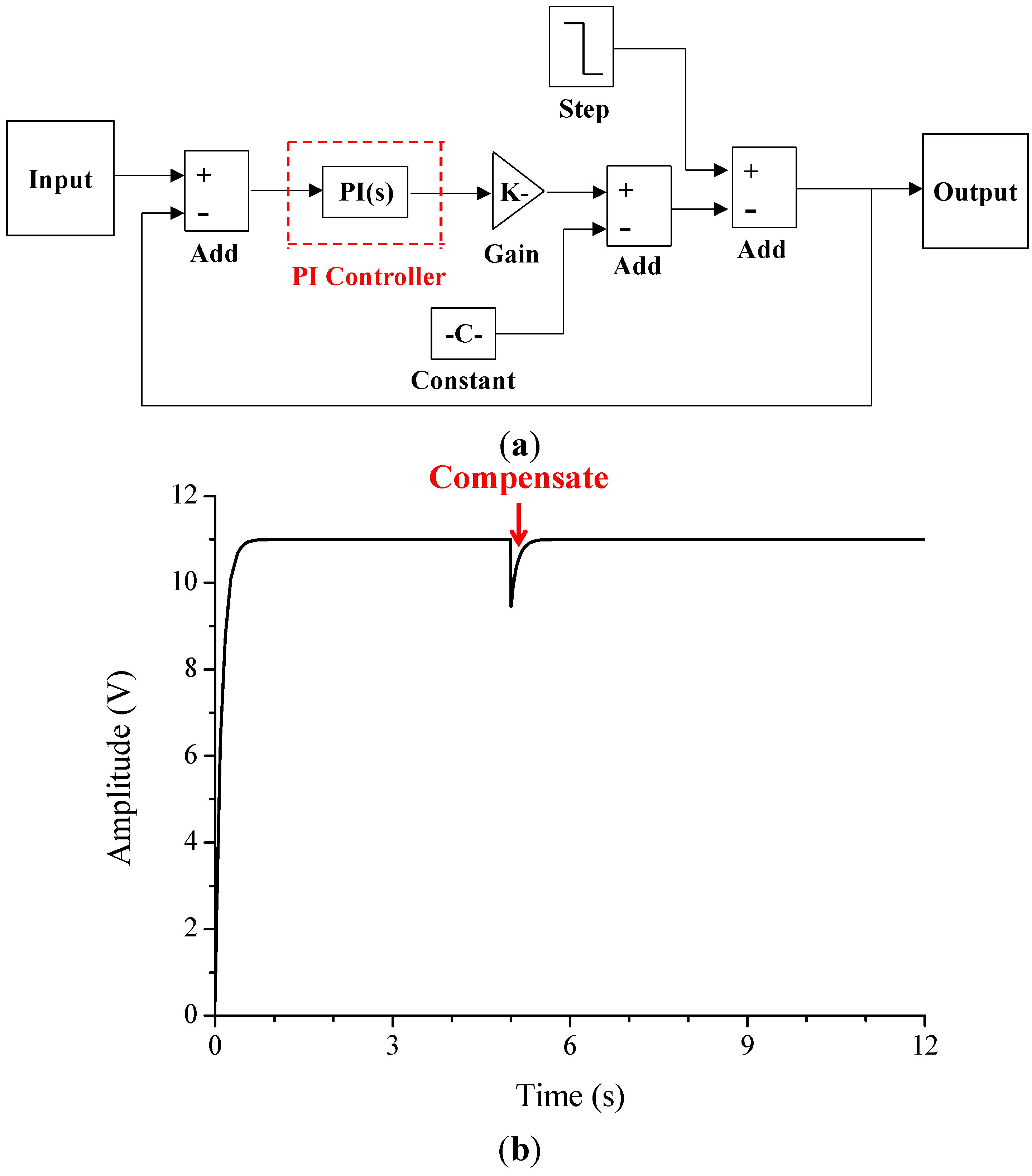
2.2. Control Part Design

As shown in Figure 1, the control part uses three sensors to monitor the transmitter and receiver statuses, namely the coil voltage, the supply current, and the load voltage. The coil voltage is extracted by rectifying the transmitter coil voltage via a high-impedance path using a half-wave rectifier. The voltage is then stepped down to a workable voltage via a voltage divider. To mitigate the loading effects and high-frequency noise, a buffer amplifier using an operation amplifier (Op-Amp) is used before the NI DAQ-6008 board’s ADC port. Next, the supply current is extracted via the current-sensing resistor Rsense in Figure 2. Rsense is located on the high side before Lchoke. The voltage drop across Rsense is stepped up via a non-inverting Op-Amp. These two sensors can monitor the transmitter status. Finally, the load voltage that monitors the receiver status is directly extracted from Rload via a high-impedance path. In Figure 4, we show a detailed schematic of the three sensors. The coil voltage sensor in Figure 4a is placed on a transmitter coil so that the transmitter’s output voltage can be monitored. Two capacitors are used to monitor the coil voltage without power loss, and the diode is used to rectify the voltage variation. The supply current sensor in Figure 4b consists of a differential amplifier and a Sallen-key low pass filter (LPF). The differential amplifier amplifies the difference between the input plus and minus currents, and the amplified current is converted to DC via the Sallen-key LPF. The load voltage sensor in Figure 4c is located at the receiver coil so that the receiving output load power can be monitored.
Figure 4. Schematic of three sensors. (a) Coil voltage sensor. (b) Supply current sensor. (c) Load voltage sensor.
Energies 08 07677 g004
Next, we need a flexible power supply circuit to control the drain bias voltage of the class-E power amplifier. To minimize the power supply loss, this should be implemented using switching mode power supply (SMPS) architecture. The schematic of the designed DC–DC converter is shown in Figure 5a, which is implemented using the TL494 pulse width modulation (PWM) integrated circuit (IC) and IR2109 of the gate driver IC. Constant voltage of 20 V is supplied to TL494/IR2109 ICs and metal-oxide semiconductor (MOS) transistors. Vin is a input voltage from DAC module and Vout is a output voltage to class-E power amplifier in Figure 1. Surface acoustic wave (SAW) pulse with the following frequency fsw is generated at the RT and CT pins of the TL494 chipset:
f s w = 1.1 R T × C T
Then, PWM signal is generated from the C2 pin of the TL494 according to the input voltage Vin of the feedback (FB) pin. The PWM signal from TL494 goes to the IN pin of the IR2109 chipset. The IR2109 is a gate driver IC, and its output signal is generated at the HO and LO pins of IR2109. Then, the output signal goes to the MOS1 and MOS2 transistors in turn, which work symmetrically like a buck converter, and we can obtain DC voltage at the load resister Rload. The output voltage Vout varies from zero to 20 V according to the duty cycle by input voltage Vin of the TL494 chipset. Here, we should satisfy the implementation condition that the cutoff frequency fcutoff in the output of the DC–DC converter, as given below, should be greater than the SAW pulse frequency fsw in Equation (1):
f c u t o f f = 1 2 π L p × C p
The measurement result of the fabricated DC–DC converter is shown in Figure 5b, where we can see that it works correctly in accordance with the variable duty cycle. When the input voltage Vin of the TL494 FB pin varies from 1 V to 3 V, the output voltage Vout in Rload varies in a linear manner from 1.4 V to 19.5 V, respectively.
Figure 5. Circuit implementation of DC–DC converter. (a) Schematic of DC–DC converter. (b) Measurement results.
Energies 08 07677 g005

3. Power Control Experiments

Figure 6 shows the experimental setup of our software-based wireless power transfer platform. The designed circuit part is connected to the upper control part using a PC with modest processing capabilities, and all algorithms are implemented in the MATLAB/Simulink environment on the PC. Especially, the functions of hardware and software are clearly separated. Therefore all circuit-based functions, such as PWM control, are designed using hardware techniques. For example, the designed DC–DC converter is implemented using TL494 PWM IC without any digital feedback using NI. The class-E power amplifier is driven by a commercial low power clock with fixed oscillation frequency of 240 kHz. Therefore, software function can be realized simple DAQ and MATLAB/Simulink, which is, in general, widely accepted software. To verify the effectiveness of our platform, we demonstrate two types of power control experiments. The first one is an output voltage regulation using closed-loop power control, and the other is no-load or metal detection using open-loop power control.
Figure 6. Experimental setup of software-based wireless power transfer platform.
Energies 08 07677 g006

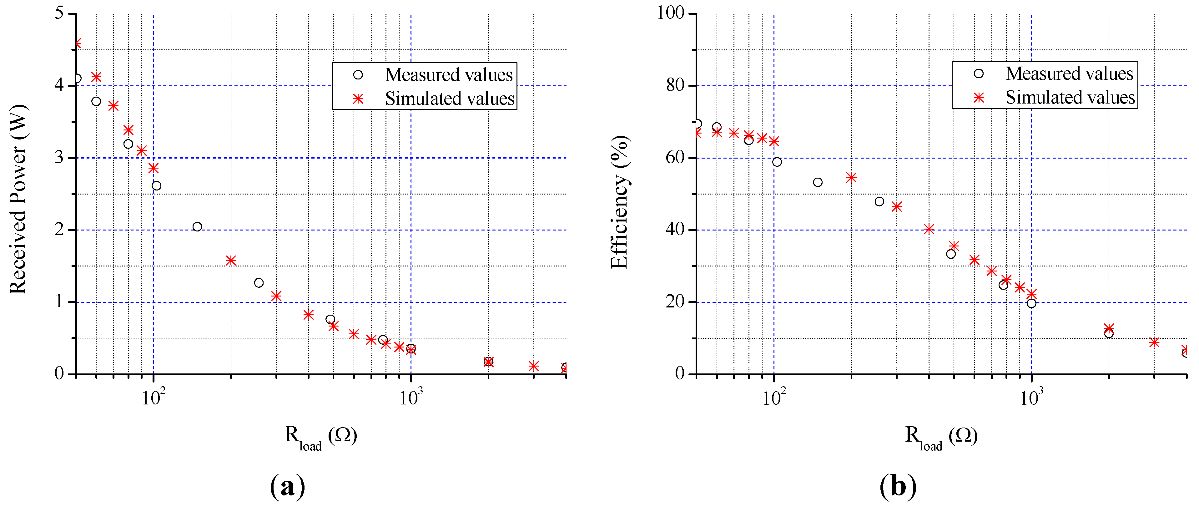
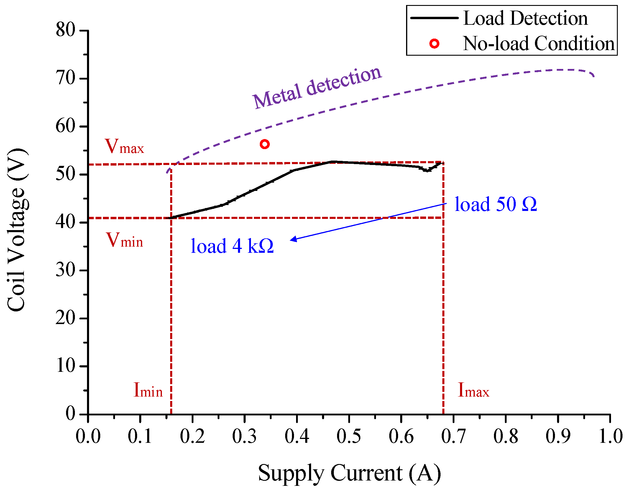
3.1. Load and Metal Detection: Open-loop Control

Figure 7 shows the space diagram of the coil voltage and supply current, which is used to detect no-load or metal objects. When any receiver coil is located on the transmitted coil, the values of the transmitter coil voltage and supply current vary with load variations. For example, the supply current decreases when the load resistor changes from 50 Ω to 4 kΩ. This is because the receiver coil does not need a large supply current for an overcharged state of 4 kΩ. However, in the metal detection case, it consumes an excessive amount of supply current and coil voltage in a short time, in the process heating metal objects. Further, our system shows the no-load condition when the operating condition is in the vicinity of the circle shape. Therefore, we can estimate the kinds of loads that exist based on the values of supply current and coil voltage on the transmitter pad. As an example, if the coil voltage is measured between 41 V (Vmin) and 52 V (Vmax) and the supply current is measured between 0.16 A (Imin) and 0.68 A (Imax), we can guess the receiver coil is placed on the valid position of the transmitter coil. On the other hand, any operating condition that is not with this range is considered to be in the abnormal case. Therefore the transmitter should be powered down when there is no valid coil placed on the transmitter coil for power saving and safety purpose. If a no-load condition or metal object is detected, the power control algorithm implemented with MATLAB/Simulink software can automatically power down the DC–DC converter via the DAC of the NI DAQ-6008 board.
Figure 7. Measured result for different loading conditions on coil voltage and supply current.
Energies 08 07677 g007
As an example, Figure 8 shows a MATLAB/Simulink code block for the open-loop control of no-load or metal detection. Using two sets of sensing information (channel #2 for the coil voltage and channel #3 for the supply current), the open-loop power control algorithm is run to perform no-load or metal detection. If the input coil voltage is between Vmin and Vmax, and the input supply current is between Imin and Imax, the switch output is 5 V and the class-E power amplifier acquires the power-on status. Otherwise, the switch output is 0.5 V and the class-E power amplifier acquires the power-off status, where a switch output of 0.5 V means 0 V because MATLAB does not support an output of 0 V.
Figure 8. MATLAB/Simulink code for ON/OFF control algorithm.
Energies 08 07677 g008

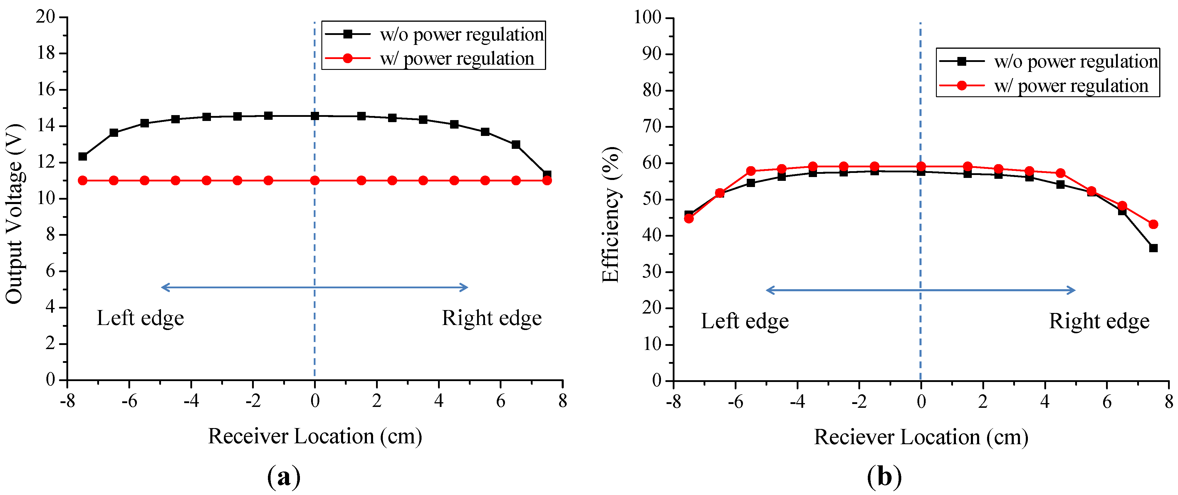
3.2. Output Voltage Regulations: Closed-Loop Control

As the receiver coil may be located at any arbitrary position over the transmitter coil surface, the received power at the receiver cannot remain constant. Changes in the received power can cause large output voltage variations. Therefore, it is necessary to stabilize the output voltage under coupling variations in a loosely-coupled planar wireless power transfer system design [23]. In this paper, we demonstrate the ability of our closed-loop power control algorithm to successfully maintain a constant receiving power. Our closed-loop power control algorithm generally works as follows: Because of the open-loop no-load detection capability, our platform starts automatically only when the receiver coil is located on the transmitter coil. After a successful load detection procedure, three sensors send the transmitter and receiver status via the ADC of the NI DAQ-6008 board. Using the sensing information, the closed-loop power control algorithm calculates the optimal bias voltage for the class-E power amplifier using MATLAB/Simulink. After performing the calculations, our proposed algorithm outputs the control voltage (Vin) for a DC–DC converter via the DAC of the NI DAQ-6008 board. Figure 9 shows a MATLAB/Simulink code block of the closed-loop power control algorithm that is used to regulate the receiver's output voltage. Using three sets of sensing information (channel 1 for the load voltage, channel 2 for the coil voltage, and channel 3 for the supply current), our algorithm adjusts the bias voltage of the class-E power amplifier in order to maintain a steady receiver power at approximately 2 W. Channel 1 for the load voltage mainly consists of the gain coefficient K, a LPF, and a proportional-integral (PI) controller. The gain coefficients (K) are used to appropriately normalize the input signals, i.e., the load voltage, coil voltage, and supply current. The PI controller is explained later in Figure 10. The information for channels 2 and 3 is obtained from the transmitter side. If the coil voltage of channel 2 is less than Vmax and the supply current of channel 3 is greater than Imin, the PI controller activates the NI DAQ analog output. Otherwise, the controller makes a decision that there is no load or metal object.
Figure 9. MATLAB/Simulink code for stabilizing receiver’s output voltage.
Energies 08 07677 g009
Figure 10a shows the block diagram for a PI controller. In this paper, we use the PI controller block of MATLAB/Simulink as the PI controller. It calculates the updated value using the proportioner and integrator as follows:
P I ( t ) = K p e ( t ) + K t 0 t e ( τ ) d τ
The PI controller monitors the output voltage and calculates the updated value after comparing the output voltage with the reference value. Figure 10b shows the measurement results of the PI controller output, which are measured through MATLAB/Simulink’s real-time scope. When there is a disturbance for a normal status of 11 V, we observe that the PI controller compensates its original value within 1 second. In this paper, we apply its compensating property to the closed-loop control of transmit power.
Figure 10. PI controller verification. (a) Block diagram for verification. (b) Measured result of time response.
Energies 08 07677 g010
Figure 11a shows the measured result of the receiver’s output voltage for different positions involving power regulation with and without closed-loop power control. We move the receiver coil from side to side and measure the voltage across Rload. In the case without output power control, the default bias voltage of the class-E power amplifier is fixed to 12 V, and the output voltages are varied owing to the coupling variation in the different receiver coil positions. On the other hand, our power control algorithm with power regulation can automatically adjust the input bias voltage of the class-E power amplifier to stabilize the output voltage. Hence, we observe a constant output voltage of 2 W for every position. In particular, our power control algorithm generates a control voltage from 1 V to 3 V. Using these control voltages, the DC–DC buck converter generates an output voltage to maintain a steady receiver power at approximately 2 W. In addition, Figure 11b shows overall system efficiency whether we use power regulation or not, and the result means that there is no efficiency degradation due to power regulation. Here, the definition of overall system efficiency is DC-to-DC efficiency, which means the ratio of total delivered output power at the load over input DC power.
Figure 11. Measured result of output voltage for different receiver positions. (a) Output voltage. (b) Efficiency.
Energies 08 07677 g011

4. Conclusions

In this paper, we proposed a software-based wireless power transfer platform using MATLAB/Simulink and an NI DAQ board for open- and closed-loop power control experiments to enable easy modification by re-writing user-level software. In order to verify the performance of our proposed software-based platform, we developed a software-based platform for experiments with two types of power control, in terms of output voltage regulation for different receiver positions and no-load or metal detection. We verified that the performance results obtained for our two experiments were acceptable when compared to those obtained using the conventional hardware-based approach. Our approach can serve as an inexpensive alternative to accurately evaluate the power control algorithm of wireless power transfer systems. Using our software-based platform, a wireless power system designer can therefore focus on the development of algorithms without the need to deal with hardware when creating real prototypes.
In future works, we need to research theoretical identification and control performance. Since we mainly focus on implementing a software-based wireless power transfer platform for various power control experiments, there exists, to an extent, a lack of theoretical background and control performance measurement. Theoretical background and measurement of control performance such as response time and overshoot will be one of our major topics for future work. In addition, improvement of power transfer efficiency will be needed for future work.

Author Contributions

Sun-Han Hwang performed the literature review, the analysis of data, and the writing and revision of the manuscript under supervision of Chung G. Kang and Byung-Jun Jang. Yong-Ho Son designed the experimental setup and carried out most of measurements and data analysis work under supervision of Byung-Jun Jang.

Conflicts of Interest

The authors declare no conflict of interest.

References

  1. Puccetti, G.; Reggiani, U.; Sandrolini, L. Experimental analysis of wireless power transmission with spiral resonators. Energies 2013, 6, 5887–5896. [Google Scholar] [CrossRef]
  2. Wei, X.; Wang, Z.; Dai, H. A critical review of wireless power transfer via strongly coupled magnetic resonances. Energies 2014, 7, 4316–4341. [Google Scholar] [CrossRef]
  3. Puccetti, G.; Stevens, C.J.; Reggiani, U.; Sandrolini, L. Experimental and numerical investigation of termination impedance effects in wireless power transfer via metamaterial. Energies 2015, 8, 1882–1895. [Google Scholar] [CrossRef]
  4. Johns, B. An introduction to the Wireless Power Consortium standard and TI’s compliant solutions. Analog Appl. J. Q 2011, 1, 10–12. [Google Scholar]
  5. Krikidis, I.; Timotheou, S.; Nikolaou, S.; Zheng, G.; Ng, D.W.K.; Schober, R. Simultaneous wireless information and power transfer in modern communication systems. IEEE Commun. Mag. 2014, 52, 104–110. [Google Scholar] [CrossRef] [Green Version]
  6. Ng, D.W.K.; Schober, R. Secure and green SWIPT in distributed antenna networks with limited backhaul capacity. IEEE Trans. Wirel. Commun. 2015. [Google Scholar] [CrossRef]
  7. Low, Z.N.; Casanova, J.J.; Maier, P.H.; Lin, J. Method of load/fault detection for loosely coupled planar wireless power system with power delivery tracking. IEEE Trans. Ind. Electron. 2010, 57, 1478–1486. [Google Scholar]
  8. Zhong, W.X.; Hui, S.Y.R. Maximum energy efficiency tracking for wireless power transfer systems. IEEE Trans. Power Electron. 2015, 30, 4025–4034. [Google Scholar] [CrossRef]
  9. Fu, M.; Yin, H.; Zhu, X.; Ma, C. Analysis and tracking of optimal load in wireless power transfer systems. IEEE Trans. Power Electron. 2015, 30, 3952–3963. [Google Scholar] [CrossRef]
  10. Yin, J.; Lin, D.; Lee, C.K.; Hui, S.Y.R. A systematic approach for load monitoring and power control in wireless power transfer systems without any direct output measurement. IEEE Trans. Power Electron. 2015, 30, 1657–1667. [Google Scholar] [CrossRef]
  11. Chaimanonart, N.; Zimmerman, M.D.; Young, D.J. Adaptive RF power control for wireless implantable bio-sensing network to monitor untethered laboratory animal real-time biological signals. In Proceedings of the 2008 IEEE Sensors Conference, Lecce, Italy, 26–29 October 2008; pp. 1241–1244.
  12. Wang, G.; Liu, W.; Sivaprakasam, M.; Kendir, G.A. Design and analysis of an adaptive transcutaneous power telemetry for biomedical implants. IEEE Trans. Circuits Syst. 2005, 52, 2109–2117. [Google Scholar] [CrossRef]
  13. Kim, J.; Choi, W.S.; Jeong, J. Loop switching technique for wireless power transfer using magnetic resonance coupling. Prog. Electromagn. Res. 2013, 138, 197–209. [Google Scholar] [CrossRef]
  14. Si, P.; Hu, A.P.; Hsu, J.W.; Chiang, M.; Wang, Y.; Malpas, S.; Budgett, D. Wireless power supply for implantable biomedical device based on primary input voltage regulation. In Proceedings of the 2nd IEEE Conference on Industrial Electronics and Applications, Harbin, China, 23–25 May 2007; pp. 235–239.
  15. Jang, B.J.; Lee, S.; Yoon, H. HF-band wireless power transfer system: Concept, issues, and design. Prog. Electromagn. Res. 2012, 124, 211–231. [Google Scholar] [CrossRef]
  16. Kiani, M.; Ghovanloo, M. An RFID-based closed-loop wireless power transmission system for biomedical applications. IEEE Trans. Circuits Syst. II Express Briefs 2010, 57, 260–264. [Google Scholar] [CrossRef] [PubMed]
  17. Restle, R.C. Choosing between DSPs, FPGAs, μPs and ASICs to implement digital signal processing. In Proceedings of the ICSPAT: DSP World, Dallas, TX, USA, 16–19 October 2000.
  18. Sudhakar, Y. VHDL Starter’s Guide; Prentice-Hall: Upper Saddle River, NJ, USA, 1998. [Google Scholar]
  19. Kruger, H.; Lotter, T.; Enzner, G.; Vary, P. A PC based platform for multichannel real-time audio processing. In Proceedings of the International Workshop on Acoustic Echo and Noise Control (IWAENC2003), Kyoto, Japan, 8–11 September 2003; pp. 195–198.
  20. Low, Z.N.; Chinga, R.A.; Tseng, R.; Lin, J. Design and test of a high-power high-efficiency loosely coupled planar wireless power transfer system. IEEE Trans. Ind. Electron. 2008, 56, 1801–1812. [Google Scholar]
  21. Raab, F.H. Effects of circuit variations on the class E tuned power amplifier. IEEE J. Solid-State Circuits 1978, 13, 239–247. [Google Scholar] [CrossRef]
  22. Casanova, J.J.; Low, Z.N.; Lin, J.; Tseng, R. Transmitting coil achieving uniform magnetic field distribution for planar wireless power transfer system. In Proceedings of the IEEE Radio Wireless Symposium (RWS’09), San Diego, CA, USA, 18–22 January 2009; pp. 530–533.
  23. Casanova, J.J.; Low, Z.N.; Lin, J. Design and optimization of a Class-E amplifier for a loosely coupled planar wireless power system. IEEE Trans. Circuits Syst. II Express Briefs 2009, 56, 830–834. [Google Scholar] [CrossRef]

