Article

Ultrafine-Grained Precipitation Hardened Copper Alloys by Swaging or Accumulative Roll Bonding

1
Central Laboratory, Research & Development, Wieland-Werke AG, Graf-Arco-Str. 36, 89079 Ulm, Germany
2
Institute of Materials Science and Engineering, TU Clausthal, Agricola-Str. 6, 38678 Clausthal-Zellerfeld, Germany
*
Author to whom correspondence should be addressed.
Metals 2015, 5(2), 763-776; https://doi.org/10.3390/met5020763
Submission received: 30 March 2015 / Revised: 7 May 2015 / Accepted: 8 May 2015 / Published: 13 May 2015
(This article belongs to the Special Issue Ultrafine-grained Metals)

Abstract

:
There is an increasing demand in the industry for conductive high strength copper alloys. Traditionally, alloy systems capable of precipitation hardening have been the first choice for electromechanical connector materials. Recently, ultrafine-grained materials have gained enormous attention in the materials science community as well as in first industrial applications (see, for instance, proceedings of NANO SPD conferences). In this study the potential of precipitation hardened ultra-fine grained copper alloys is outlined and discussed. For this purpose, swaging or accumulative roll-bonding is applied to typical precipitation hardened high-strength copper alloys such as Corson alloys. A detailed description of the microstructure is given by means of EBSD, Electron Channeling Imaging (ECCI) methods and consequences for mechanical properties (tensile strength as well as fatigue) and electrical conductivity are discussed. Finally the role of precipitates for thermal stability is investigated and promising concepts (e.g. tailoring of stacking fault energy for grain size reduction) and alloy systems for the future are proposed and discussed. The relation between electrical conductivity and strength is reported.

1. Introduction

Precipitation hardening can provide a combination of high strength and high (thermal or electrical) conductivity in copper alloys. By concentrating the alloying elements in fine precipitates, the Cu-matrix remains relatively pure with only few interstitial or substitutional atoms left in the Cu-matrix. Consequently conductivity is not detrimentally affected by solid solution impurities while maintaining high yield strength by finely dispersed precipitates which effectively impede dislocation movement.
The industrially most relevant precipitation hardened copper alloys combining high strength with high electrical conductivity are essentially Corson-alloys [1] which are often (but not exclusively) based on the ternary system Cu-Ni-Si. The Cu-Ni-Si-system has been thoroughly studied already in 1927 [1]. Microstructurally, the high yield strength (up to 800–900 MPa after precipitation hardening and cold working) is caused by finely dispersed semi-coherent Ni-Si-precipitates [2,3] with a diameter lower than 20 nm. As explained by the phase diagram (Figure 1), the temperature of solution annealing strongly depends on the amount of alloyed Ni and Si. Today, preferred and standardized alloys such as C7025 or C7035 contain ~3% silicides.
Figure 1. Pseudo-binary phase diagram of the Cu-Ni2Si-system after Corson, 1927 [1].
Metals 05 00763 g001
The traditional approach for the development of high strength copper alloys is focused on chemical variation of precipitation hardened alloys [4]. In addition, microstructural control, e.g., generation of very fine grained or even ultra fine grained copper alloys, opens the door for tailored copper alloys combining optimized precipitate- as well as grain- or subgrain structure. Both approaches are presently used to generate high-performance components for industrial practice. Common methods for generating ultra fine grained metals by Severe Plastic Deformation (SPD), such as Equal Channel Angular Pressing (ECAP) or Accumulative Roll Bonding (ARB) [5,6,7], are well known and established, especially for pure copper. In contrast to SPD-related studies on pure copper, the archival literature sources dealing with severe plastic deformation of copper alloys are significantly more rare [8,9].
In the present study the authors seek to investigate and discuss the applicability of swaging (as a continuous method) as well as ARB for achieving very fine grained to ultra fine grained microstructures in classical Cu-Ni-Si alloys. A key feature of the research presented here is the stabilization of the microstructure by optimized aging treatments after swaging or ARB.

2. Experimental Section

The investigated copper alloy is the Corson-type alloy CuNi3Si1Mg (UNS designation C70250), which has experienced wide-spread use as connector-, leadframe- and high-strength wire material. Traces of Mg are alloyed to enhance the stress relaxation stability. Mg contributes to solid solution hardening as well as to precipitation hardening since Mg atoms may also form mixed (Ni,Mg)-silicides. The material investigated in our present study was hot extruded at 900 °C, then solution annealed at 800 °C/2 h (or alternatively at 950 °C/10 min). This condition was then rotary swaged and finally precipitation hardened. It should be noted that a complete dissolution of coarse Ni-silicides is not possible at these temperatures [10]. In the present study, the precipitation hardening was carried out at 450 °C.
Backscatter (ECCI, electron channeling contrast imaging) electron microscopy [11,12] was carried out using an AsB (Angle Selective Detector, Zeiss, Oberkochen, Germany) [13] in a Zeiss ULTRA scanning electron microscope (SEM, Zeiss, Oberkochen, Germany) equipped with a thermal field emission cathode. Typically, an aperture lens of 120 µm and acceleration voltages of 15–20 kV at a working distance of 2–6 mm were used.
For the Electron Backscatter Diffraction (EBSD) investigations, an EBSD-unit by Oxford was used. The EBSD patterns were recorded using a 4 × 4 binning, data acquisition and calculation of the patterns were performed by a Nordlys camera and AZTEC software by Oxford (UK), respectively. Prior to EBSD and ECCI-characterization in the SEM, the samples were carefully mechanically ground up to 2400 grid (SiC paper) and then polished up to 1 µm. Finally, samples were vibration polished for 3 h with dispersed magnesium oxide to aim for a sample surface with as little preparational cold work as possible. Two sets of experiments were carried out: swaging (which was carried out at TU Clausthal, Clausthal-Zellerfeld, Germany) of solution annealed bars from an initial diameter of 24 mm to a diameter of 7 mm (phi = −2.4) as well as swaging of a solution annealed wire with a diameter of 5.3 mm to a diameter of 2.7 mm (phi = −1.39). In both cases, precipitation annealing after swaging was done at 450 °C at different aging times. In the following elaborations we will use the terminology “peak-aged” for samples which were precipitation hardened at 450 °C for 1–6 h and “over-aged” for samples which were precipitation hardened for >16 h. Further details concerning the aging kinetics for the 2.7 mm wire are given in [14]. Finally, the swaged and subsequently precipitation hardened samples were mechanically characterized by tensile- and hardness tests. Moreover, the electrical conductivity of all the samples, before and after artificial aging, was measured using a SIGMATEST@-probe (eddy current method, Foerster, Reutlingen, Germany).

3. Results and Discussion

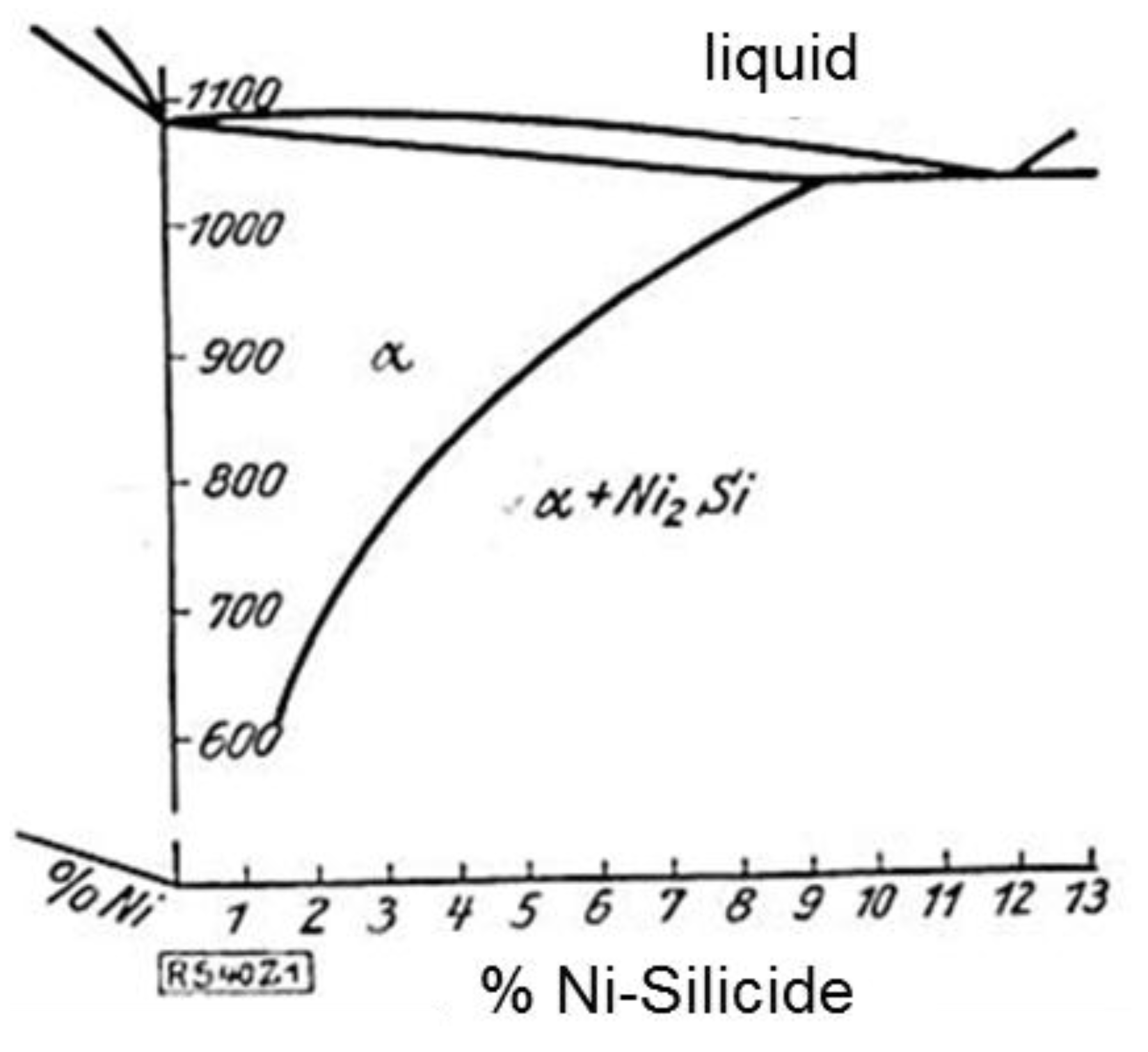
CuNi3Si1Mg was hot extruded at 800–900 °C, then solution treated at 800 °C/2 h (or alternatively 950 °C/10 min) and subsequently water-quenched. After this treatment the alloy exhibited a coarse grained microstructure with grain sizes of 100–150 µm and a few coarse silicides (typical diameter of a few hundred nm) which were not completely dissolved during homogenization.
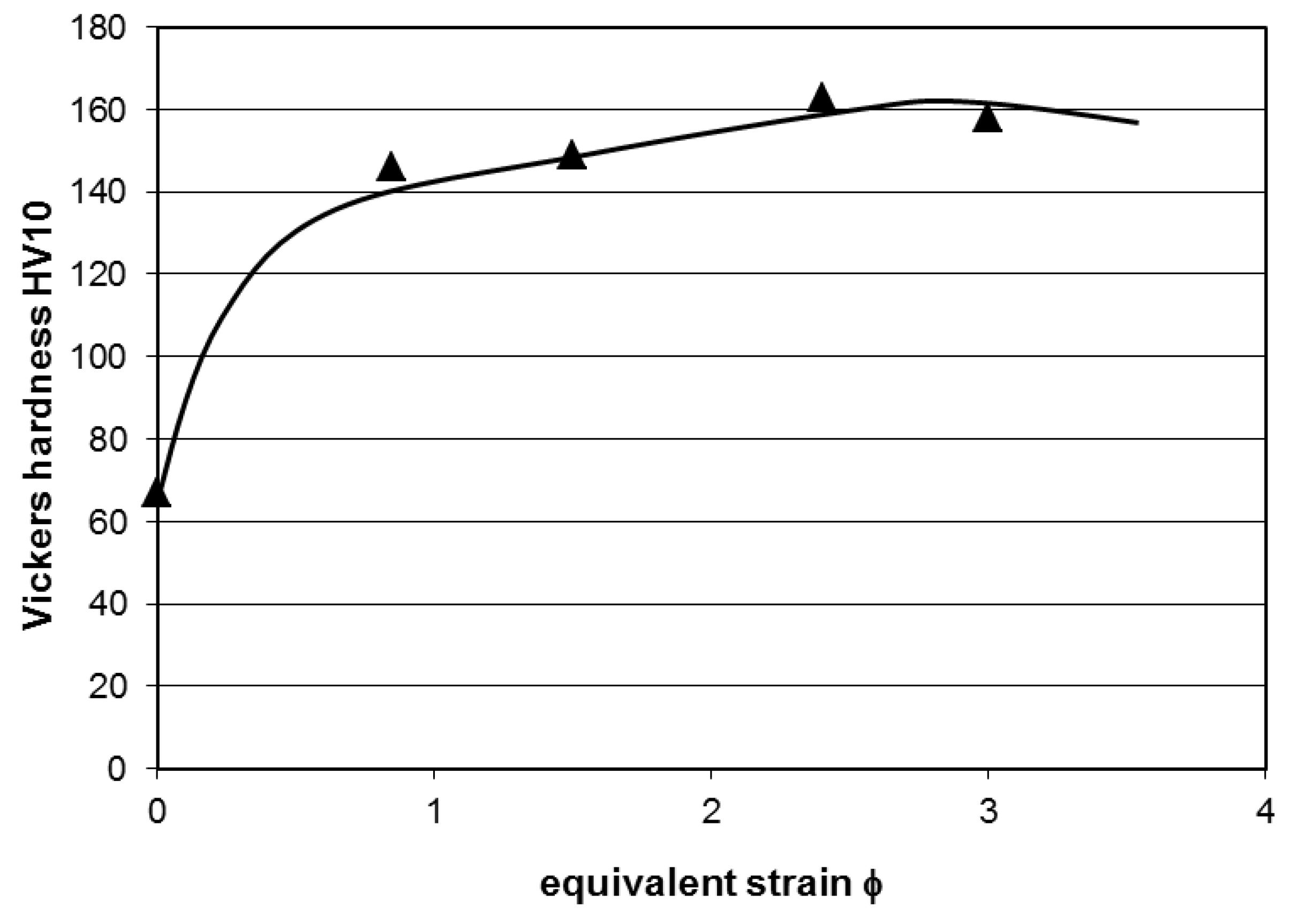
The strain hardening curve for the solution treated and swaged condition can be seen in Figure 2. The highest hardness increase was observed after swaging up to a logarithmic strain of 2.5, then some saturation or even slight softening takes place. Therefore, further investigations focused on the condition swaged to a strain of 2.5, corresponding to a hardness increase of 100 HV as compared to the solution annealed state.
Figure 2. Hardness evolution of solution treated CuNi3Si1Mg by swaging.
Metals 05 00763 g002
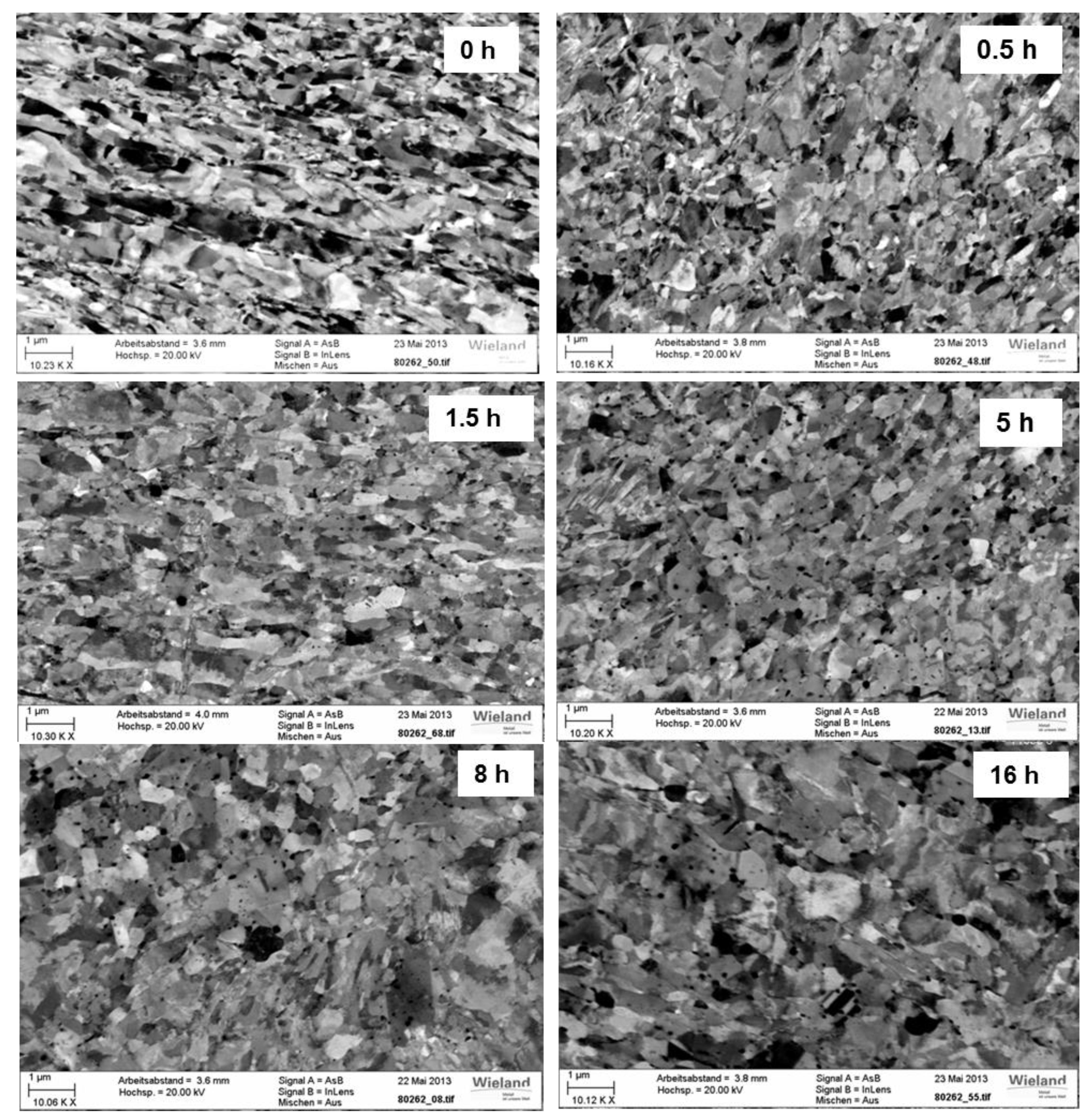
After the extruded and solution treated bars were swaged from a diameter of 24 mm down to a diameter of 7 mm, an artificial aging treatment at 450 °C for aging times ranging from 30 min to 16 h was carried out. Figure 3 exhibits the resulting ultra fine grained microstructure at high resolution (magnification ~10000 times) before and after aging (distance from surface 100 µm). The swaging treatment significantly reduced the grain- or subgrain size to 200–800 nm. In addition, the formed ultra-fine grains show some pronounced elongation. With increasing distance from surface the grains become more equiaxed and their size increased up to ~2 µm in the center of the swaged bar. With increasing aging time, characteristic structural changes can be observed in the grain- and precipitate size- and arrangement (Figure 3). More and more precipitates (presumably largely Ni2Si [10]) are formed as the aging continues, until, after 5–6 h at 450 °C a maximum hardness increase (peak-aging) occurs (see also Figure 4 and Figure 6). By then, the grains have become more equiaxed in shape, however the grain coarsening is still not very pronounced. The precipitates are mainly concentrated on grain boundaries (Figure 3, 5 h). Only after extended aging of 16 h at 450 °C (Figure 3, 16 h) the microstructure becomes over-aged with clearly coarser grains as well as coarse precipitates, leading to a decline of hardness also. In this context, the characteristic sizes of the precipitates in the peak-aged and over-aged condition have to be pointed out.
Figure 3. Microstructure of swaged CuNi3Si1Mg after different aging times (T = 450 °C) (ECCI-micrographs).
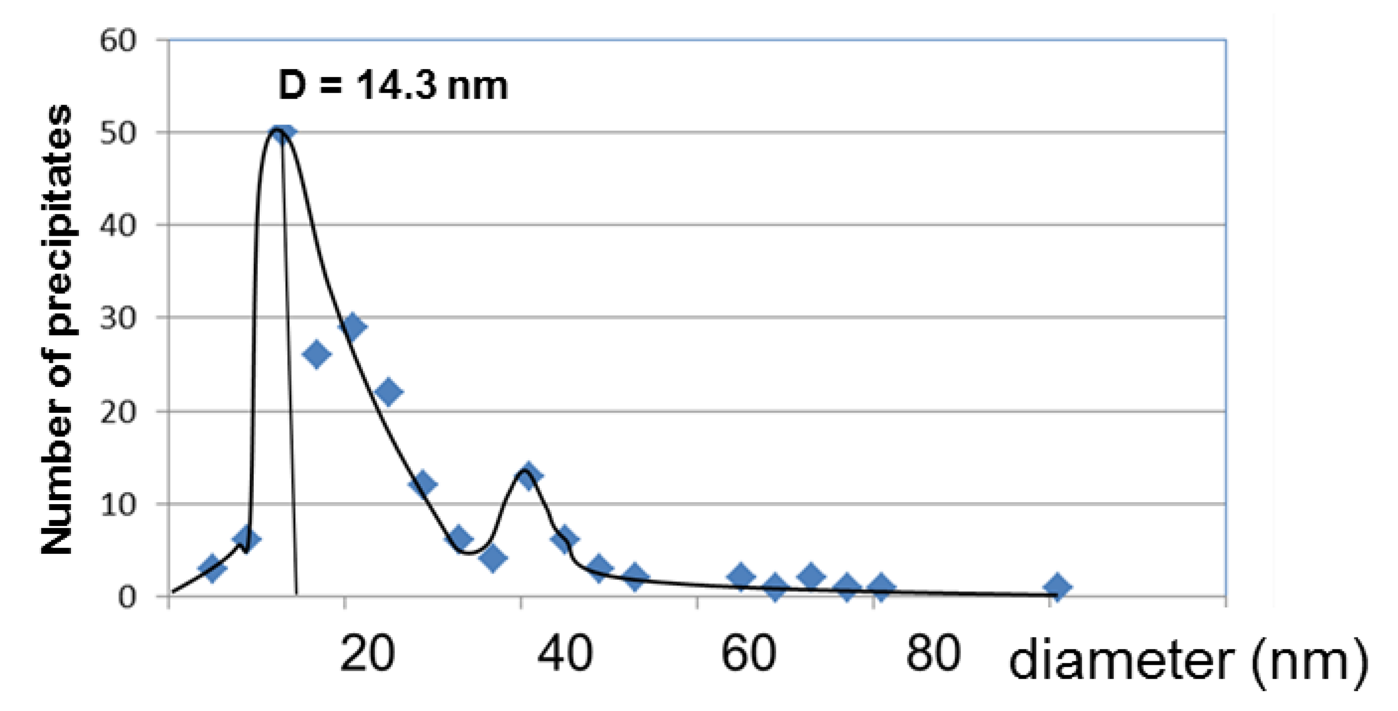
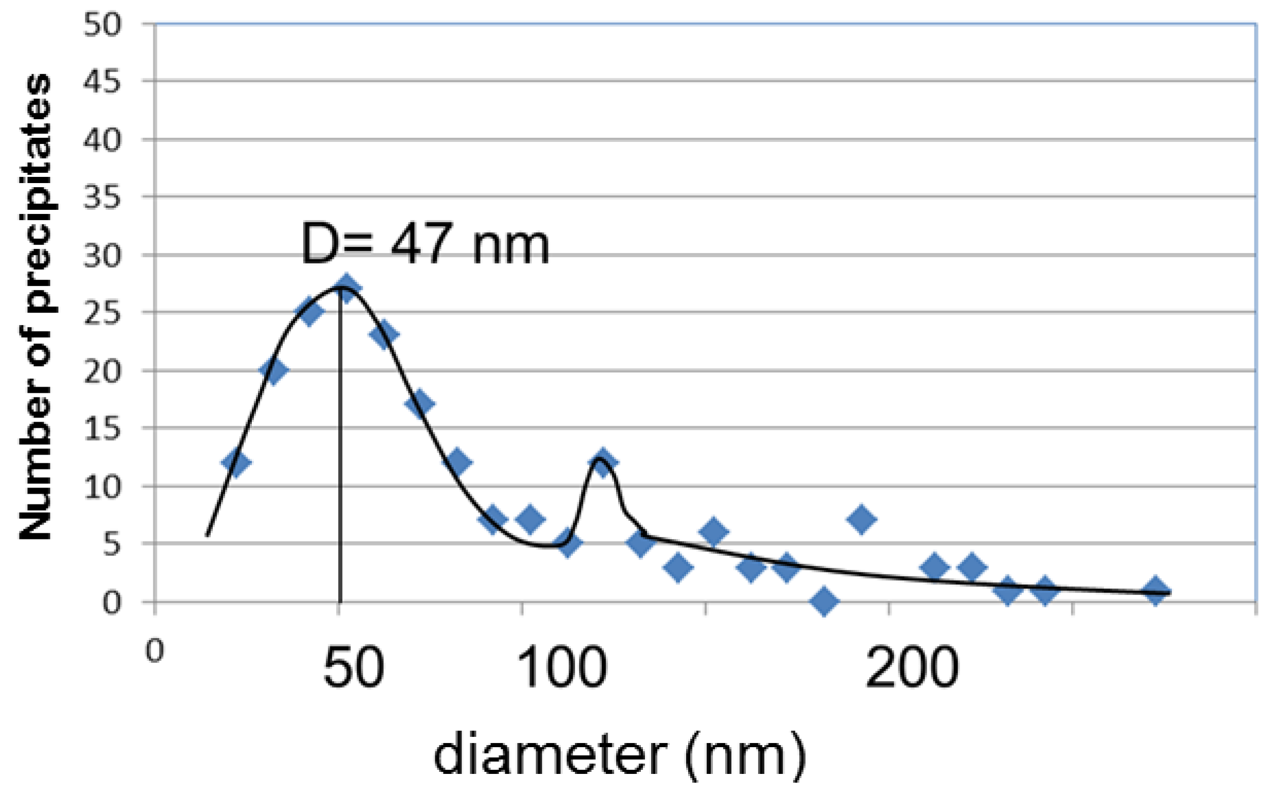
Metals 05 00763 g003
Figure 4 and Figure 5 illustrate the size distribution of the precipitates in the peak-aged and over-aged condition, as derived from manual counting and measuring of precipitates in Electron Channeling Contrast Imaging (ECCI)–SEM micrographs. At the hardness peak (peak-aging) the average precipitate diameter is around 14 nm, whereas in the over-aged condition, after 16 h, the average precipitate diameter increased to around 47 nm. These aging kinetics are 3 to 5 times faster than in the non-swaged condition where a hardness maximum is found after 16 hours accompanied by typical mean precipitate diameters of 5 nm (see also [2] for comparison). Interestingly, for both conditions, peak-aged as well as over-aged, a bimodal precipitate size distribution was detected (Figure 4 and Figure 5). By means of Energy Dispersive Spectroscopy (EDS) microanalysis we can not distinguish between nanoscale orthorhombic Ni2Si and the possible hexagonal minority phase Ni31Si12 (which is thermodynamically expected for low Ni-content of ~2%). From measurements using EBSD, it appeared that there is also a fraction of hexagonal Ni-silicides. If this observation is any evidence of Ni31Si12-phase in addition to Ni2Si, it is likely that the bimodal size distribution is also driven by this second type of precipitation. Alternatively, it can also be speculated, that the bimodal size distribution is possibly caused by different aging kinetics of precipitates at or near grain/subgrain boundaries and within the grains where diffusion is drastically different.
Figure 4. Precipitate size distribution in the peak-aged condition.
Metals 05 00763 g004
Figure 5. Precipitate size distribution in the over-aged condition.
Metals 05 00763 g005
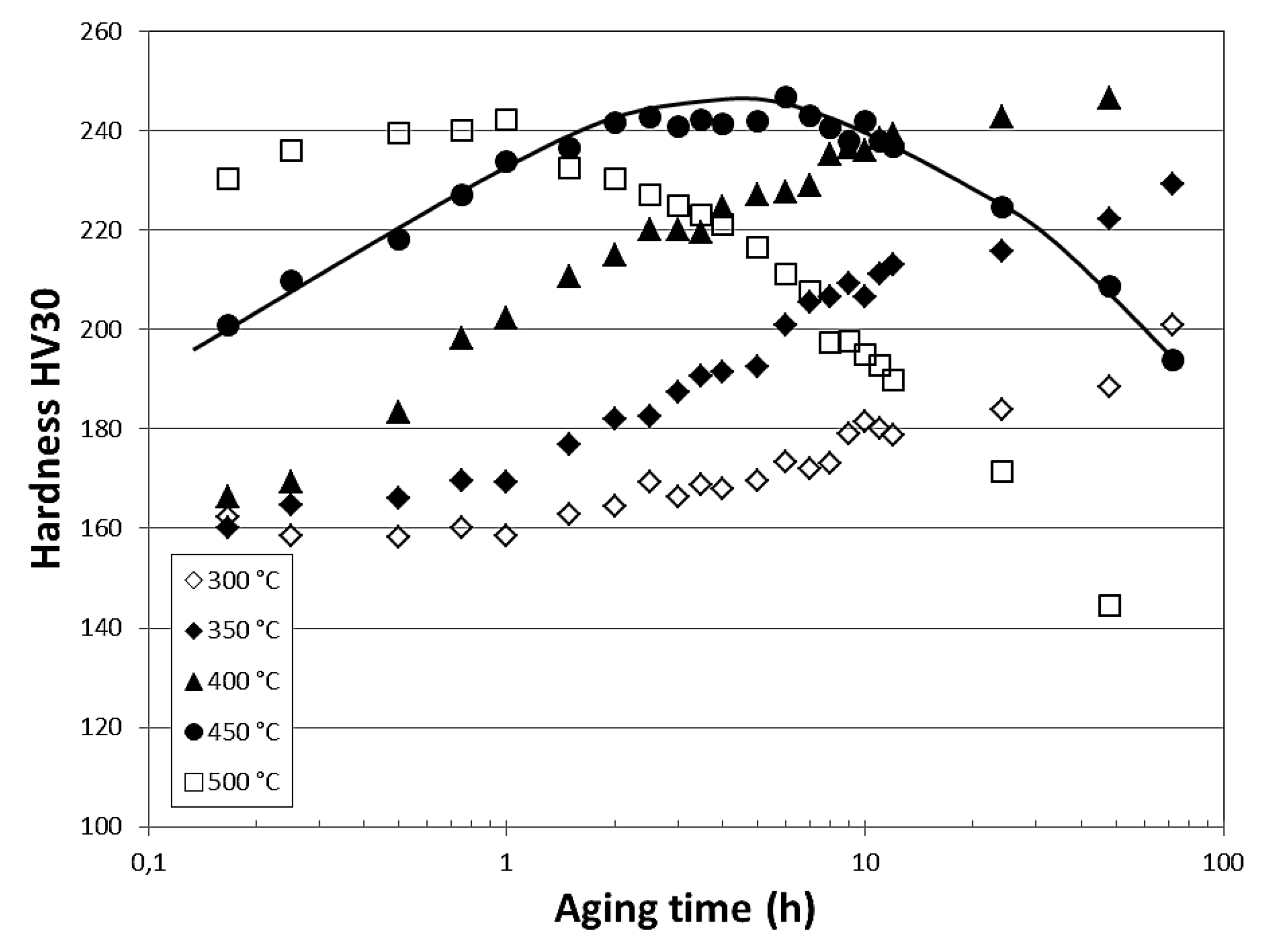
Figure 6 exhibits the aging curves (hardness vs. aging time) of swaged CuNi3Si1Mg for isothermal aging in the temperature range 300–500 °C. Hardness values of up to 245 HV can be reached in the peak-aged conditions at aging temperatures of 400, 450 or 500 °C. With increasing temperature the hardness peak is shifted to smaller aging times. At an aging temperature of 350 °C, only a maximum hardness of ~230 HV appears to be possible.
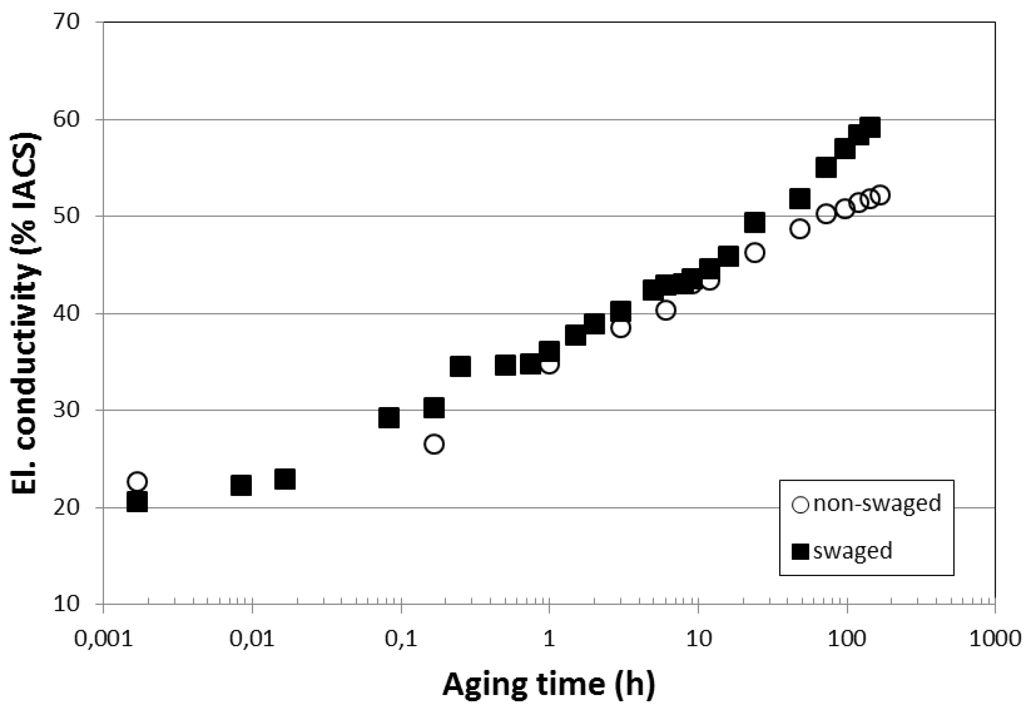
Figure 7 shows the change of electrical conductivity of the swaged and non-swaged condition during aging at 450 °C. The diffusion of the alloying elements Ni and Si from the solid solution into the precipitates decreases the scattering of electrons by the strain fields of solute atoms. As a result, the electrical conductivity increases.
Figure 6. Aging curves of swaged CuNi3Si1Mg for different aging temperatures.
Metals 05 00763 g006
Figure 7. Conductivity vs. aging time for swaged (UFG) and coarse-grained CuNi3Si1Mg (T = 450 °C).
Metals 05 00763 g007
It is noteworthy, that already after 10 min the conductivity of the swaged condition is slightly higher than the conductivity of the non-deformed condition at this temperature. Obviously, the diffusion of solute elements is significantly accelerated by fast diffusion paths such as high- and low angle boundaries which are prevalent in the swaged condition. Throughout the further aging process the electrical conductivity of the swaged condition stays superior to the conductivity of the non-deformed condition. This difference amounts up to 8% IACS (International Annealed Copper Standard, 58 MS/m) in severely over-aged specimens, possibly being caused also by recrystallization which drastically reduces the grain boundary area in the swaged and severely over-aged condition. For comparison, standardized commercial CuNi3Si1Mg strips typically have electrical conductivities of 35%–45% IACS.
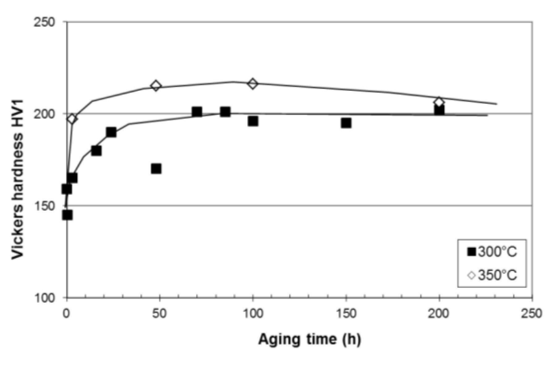
At an aging temperature of 450 °C, the microstructure of the swaged condition was not stable for long aging times. Nevertheless, at a lower aging temperature of 300 °C an aging effect can be induced without pronounced over-aging. At this temperature, a drop of hardness is not observed within several hundred hours thermal exposure (Figure 8). For the application of electromechanical connectors, this is a significant finding, since electromechanical connectors (in the presented conductivity range) are usually not exposed to temperatures higher than 150–200 °C during service. At this moment, implications for stress relaxation behavior of swaged or severely deformed precipitation hardened Corson-alloys remain speculative, however it can be assumed, that finely precipitated Ni-silicides at grain boundaries as well as within grains may also serve to effectively diminish stress relaxation or creep.
Figure 8. Hardness evolution of swaged CuNi3Si1Mg during thermal exposure at 300 °C (specimens swaged from 5.3 to 2.7 mm diameter).
Metals 05 00763 g008
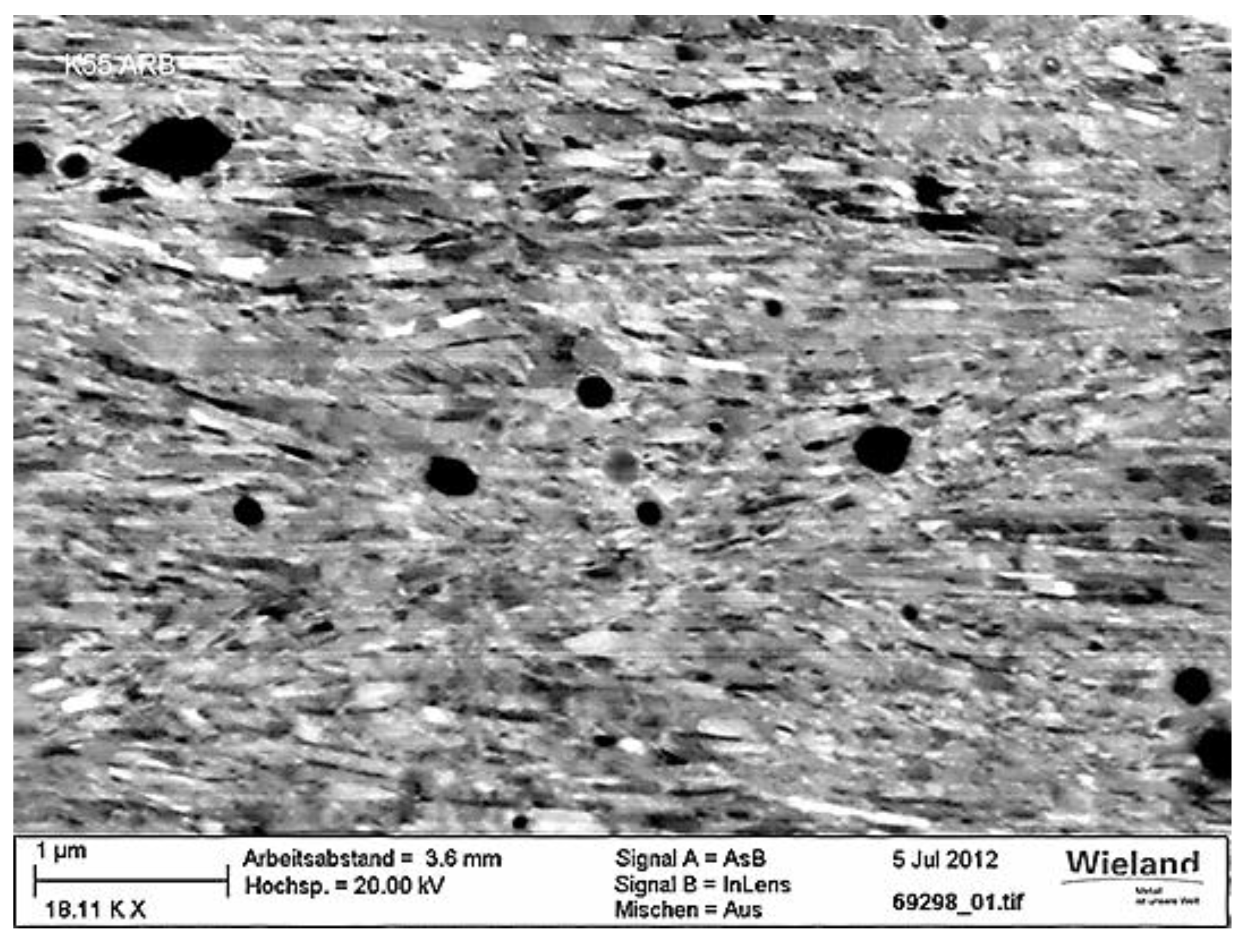
As aforementioned, no homogeneous ultrafine grained (UFG) structure was achieved by swaging CuNi3Si1Mg bars from diameters of 24 mm to 7 mm. However, for wire which was swaged from 5.3 to 2.7 mm, a fully ultra fine grained structure was observed in the whole cross section after swaging and subsequent aging. Figure 9 and 
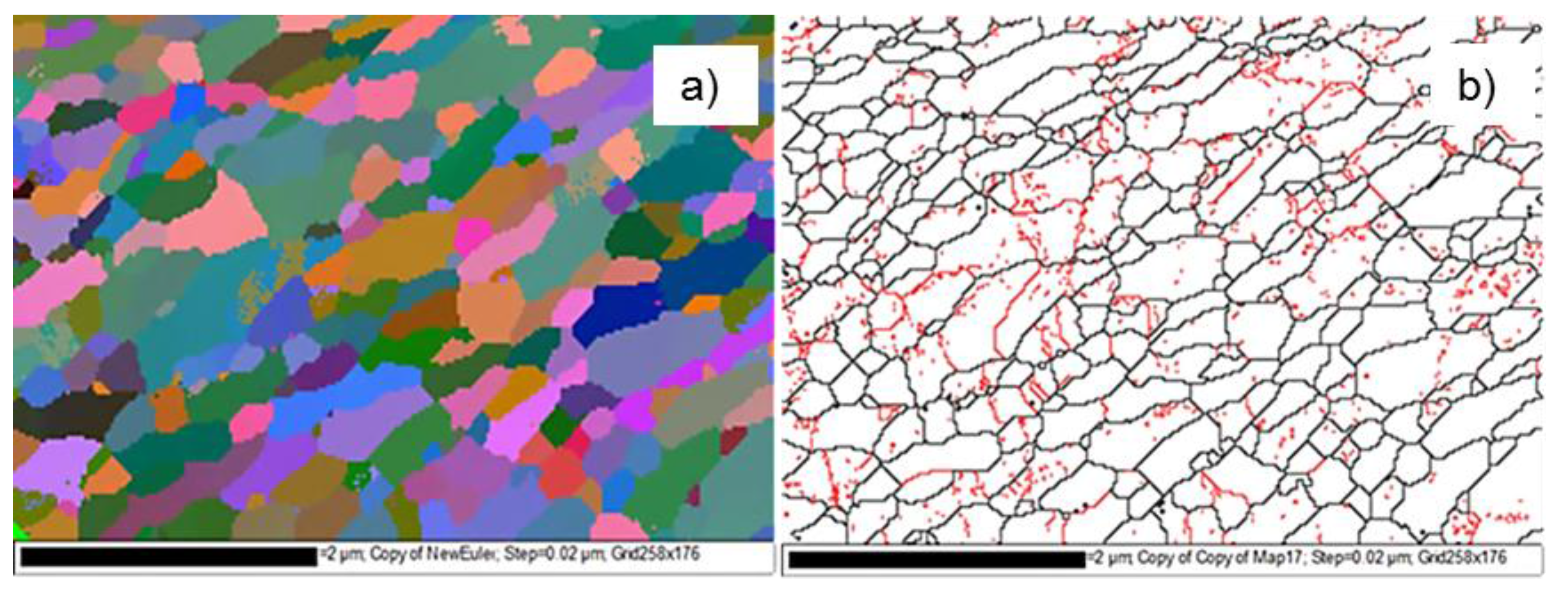
Figure 10 show ECCI- as well as EBSD results for the obtained microstructure after aging at 450 °C for one hour. This microstructure (pictured in the center of the specimen) is characterized by strong orientation contrast (Figure 9), rather low dislocation density within the grains and a high percentage of high-angle boundaries (as seen by mapping grain orientations (Figure 10a) and grain boundary misorientations (Figure 10b) using EBSD). The typical resulting grain size in this UFG structure is about 350 nm.
Figure 9. ECCI-picture of ultra-fine grained CuNi3Si1MgSi (swaged and aged at 450 °C/1 h, swaging from diameter of 5.3 to 2.7 mm).
Metals 05 00763 g009
Figure 10. Fully ultra-fine grained CuNi3Si1Mg Electron Backscatter Diffraction Pattern (EBSD) orientation mapping showing Euler-orientations (a) and grain boundaries (b). High-angle grain boundaries are depicted in black, Low-angle grain boundaries are depicted in red).
Metals 05 00763 g010
Ultra fine grained microstructures can be obtained also in CuNi3Si1Mg by accumulative roll bonding (ARB) [15]. 
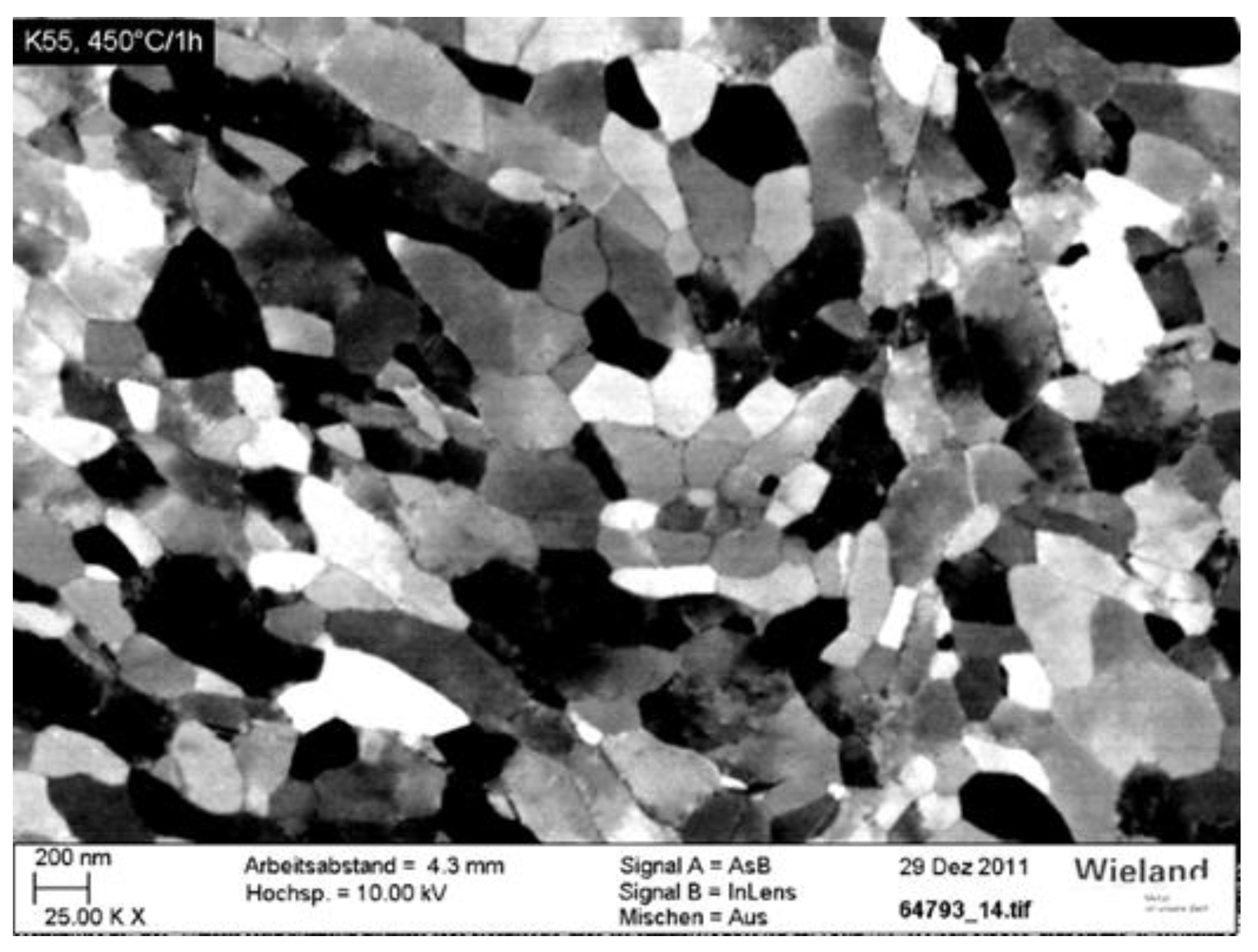
Figure 11 shows a high resolution ECCI micrograph of ARB-processed CuNi3Si1Mg. (for details see [15]). The typical microstructure of ARB-processed CuNi3Si1Mg is characterized by elongated grains perpendicular to rolling direction, having grain diameters lower than 200 nm. An analysis of high angle grain boundaries by EBSD reveals a grain width of 100 nm. This corresponds to other findings [16], where for the same logarithmic strain of ~5, ARB-processed pure copper showed similar grain widths. Also here, aging experiments after severe plastic deformation were carried out. In analogy to the swaged condition, precipitates were formed preferentially at grain boundaries, thus reducing the grain boundary mobility during further thermal exposure.
Figure 11. Microstructure of solution treated ARB-processed CuNi3Si1Mg. The larger precipitates were not dissolved by the solution treatment and are remains from the prematerial as produced by continuous casting.
Metals 05 00763 g011
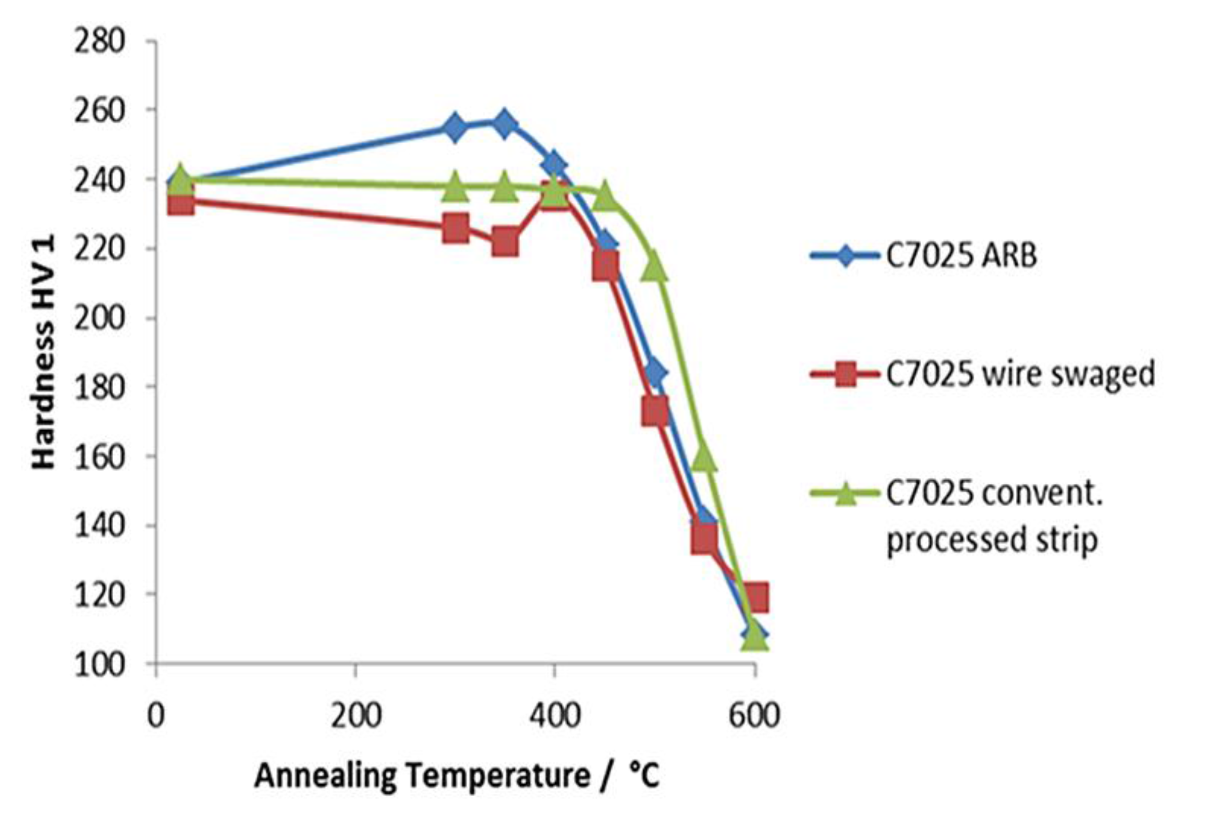
Figure 12 exhibits a thermal softening curve (hardness vs. temperature) of differently processed CuNi3Si1Mg after 1 hour annealing at 300 to 600 °C. If we define the onset of softening as a loss of 10% in initial hardness, the conventionally processed spring hard strip softens at 500 °C whereas the swaged and ARB conditions start softening at 475 °C. This thermal stability is significantly higher compared to pure copper, where softening in the ARB condition already starts at 200 °C [17]. By using high resolution ECCI, grain boundary pinning by Ni2Si-precipitates is confirmed as the underlying mechanism for the high thermal stability (Figure 13).
Figure 12. Thermal stability of swaged and ARB-processed CuNi3Si1Mg as compared to conventional strip.
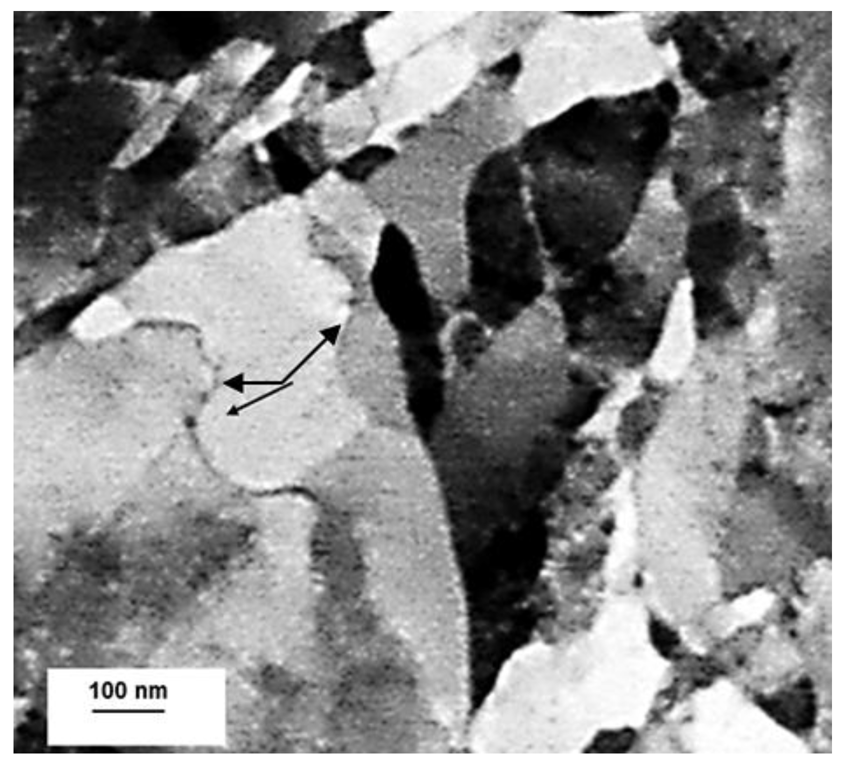
Metals 05 00763 g012
Figure 13. ECCI-micrograph of swaged and under-aged CuNi3Si1Mg showing a low-angle grain boundary which is pinned by Ni-silicides (arrows).
Metals 05 00763 g013
The resulting mechanical (quasistatic as well as cyclic) properties after severe plastic deformation and optimized aging treatments are significantly superior to conventionally processed strip. As an example, thin CuNi3Si1Mg wires (diameter 0.1 mm) which were processed from swaged and optimized aged bars show tensile strengths of up to 1050 MPa and yield strengths higher than 1000 MPa. However, this strength increase is achieved at the expensive of electrical conductivity which is reduced to less than 25% IACS.
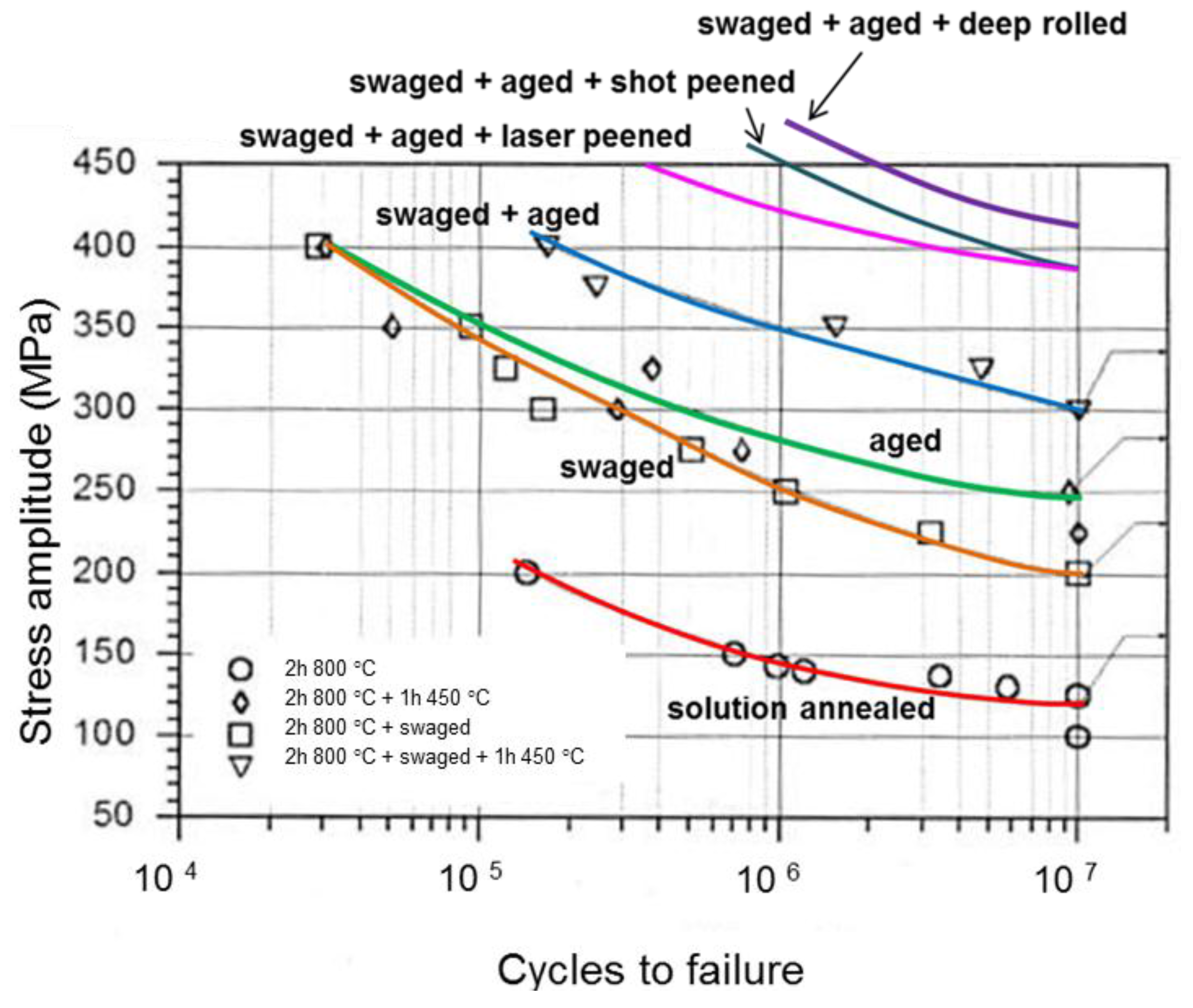
In addition to excellent quasistatic strength, optimized swaging plus consecutive aging leads to a marked increase of the 107-fatigue endurance strength from 250 to 300 MPa (Figure 14). By combining these processes with a final mechanical surface treatment (such as shot peening, laser peening or deep rolling) even higher fatigue strengths of about 400 MPa can be achieved [18]. Higher fatigue strengths for copper alloys are only reported for high-alloyed spray-formed copper alloys and Cu-Be alloys [19].
Figure 14. Wöhler-curves (rotation bending, R = −1) of swaged and non-swaged optimized precipitation hardened CuNi3Si1Mg for different mechanical surface treatments (part of this data from [18]).
Metals 05 00763 g014
As an outlook, in context with swaging the following further approaches should be addressed:
Firstly, CuNi3Si1Mg is low alloyed, therefore the achievable strength is limited by the volume fraction of the precipitates. To enable highest strengths of CuNi3Si1Mg, significant cold work is necessary (e.g., by drawing) which in turn lowers the conductivity. Higher alloyed Cu-Ni-Si alloys or more complex alloy systems such Cu-Ni-Si-Cr or Cu-Ni-Co-Si allow higher volume fractions of precipitates or multiphase hardening, respectively. First results on swaged and aged CuNi7Si2Cr are promising and indicate possible conductivities of 34% IACS at tensile strengths of ~1100 MPa after swaging and optimized aging, which is in the strength regime of Cu-Be-alloys.
Another approach to generate UFG copper alloys is to introduce an extremely high twinning density by severe deforming of single-phased copper alloys which exhibit very low stacking fault energies (such as Cu-Al, Cu-Al-Si, Cu-Zn or Cu-Zn-Si). By finely spaced twinning a very fine grain size can be achieved after swaging leading to a hardness of more than 420 HV (which corresponds to tensile strengths higher than 1300 MPa). Figure 15 shows the refinement of the microstructure by twinning in CuAl5.8Si2 (estimated stacking fault energy around 6 mJ/m² or lower [20,21]) with increasing logarithmic deformation degree during swaging. However, CuAl5.8Si2 is non-age hardenable, therefore there are no precipitates stabilizing the grain boundaries during thermal exposure. As a consequence, a hardness loss of more than 10% is observed at 300 °C after just one hour.
Figure 15. Evolution of an ultrafine-grained structure in single phased low-stacking fault alloy CuAl5.8Si2 by swaging (Left: non-swaged; Middle: swaged to a logarithmic strain of −0.8; Right: swaged to a logarithmic strain of −1.4).
Metals 05 00763 g015

4. Conclusions

The combination of swaging and subsequent optimized precipitation hardening is a simple method to produce Cu-Ni-Si materials with very fine grain size in the range 0.2–2 µm. For strip material accumulative roll bonding (ARB) is a suitable method to generate ultra fine grained microstructures in Cu-Ni-Si alloys. A crucial role is ascribed to the artificial aging treatment after the severe plastic deformation. The thermal stability of ultra fine grained CuNi3Si1Mg is significantly enhanced as compared to pure copper, owing to nanoscopically small precipitates which effectively pin the grain boundaries during aging or annealing. At 300 °C no over-aging was detected within 200 h. For short time exposure (1 h) the grain structure is fairly stable up to 400 °C. In addition to enhanced ultimate tensile- and yield strength (with possible strength >1000 MPa), also the fatigue behavior in the High Cycle Fatigue (HCF)-regime was significantly improved by the UFG-structure in the swaged plus peak-aged condition close to the surface.

Acknowledgments

Experimental help during wire drawing of Cu-Ni-Si wire by D. Vucic-Seele is kindly acknowledged.

Author Contributions

I.A. is the primary author of the paper and performed analysis of the experimental data. M.G. and M.M. contributed to the experimental research work. H.A.K. and L.W. discussed the results and analysis with the other authors.

Conflicts of Interest

The authors declare no conflict of interest.

References

  1. Corson, M.G. Copper hardened by a new method. Z. Metallkunde 1927, 19, 370–371. [Google Scholar]
  2. Lockyer, S.A.; Noble, F.W. Precipitate structure in a Cu-Ni-Si alloy. J. Mater. Sci. 1994, 29, 218–226. [Google Scholar] [CrossRef]
  3. Wang, C.; Zhu, J.; Lu, Y.; Guo, Y.; Liu, X. Thermodynamic description of the Cu-Ni-Si system. J. Phase Equilib. Diffus. 2014, 35, 93–104. [Google Scholar] [CrossRef]
  4. Kuhn, H.-A.; Altenberger, I.; Käufler, A.; Hölzl, H.; Fünfer, M. Properties of high performance alloys for electromechanical connectors. In Copper Alloys—Early Applications and Current Performance—Enhancing Processes; Collini, L., Ed.; InTech: Rijeka, Croatia, 2012; p. 52. [Google Scholar]
  5. Valiev, R.Z.; Islamgaliev, R.K.; Alexandrov, I.V. Bulk nanostructured materials from severe plastic deformation. Prog. Mater. Sci. 2000, 45, 103–189. [Google Scholar] [CrossRef]
  6. Höppel, H.W.; May, J.; Göken, M. Enhanced strength and ductility in ultrafine-grained aluminium produced by accumulative roll bonding. Adv. Eng. Mater. 2004, 6, 781–784. [Google Scholar] [CrossRef]
  7. Mughrabi, H.; Höppel, H.W.; Kautz, M. Fatigue and microstructure of ultrafine-grained metals produced by severe plastic deformation. Scr. Mater. 2004, 51, 807–812. [Google Scholar] [CrossRef]
  8. Neishi, K.; Horita, Z.; Langdon, T.G. Achieving superplasticity in a Cu–40%Zn alloy through severe plastic deformation. Scr. Mater. 2001, 45, 965–970. [Google Scholar] [CrossRef]
  9. Wang, J.; Zhang, P.; Duan, Q.; Yang, G.; Wu, S.; Zhang, Z. Tensile deformation behaviors of Cu-Ni alloy processed by equal channel angular pressing. Adv. Eng. Mater. 2010, 12, 304–311. [Google Scholar] [CrossRef]
  10. Kinder, J.; Huter, D. TEM-Untersuchungen an höherfesten und elektrisch hochleitfähigen CuNi2Si-Legierungen. Metall 2009, 63, 298–303. [Google Scholar]
  11. Altenberger, I.; Kuhn, H.-A.; Gholami, M.; Mhaede, M.; Wagner, L. Characterization of ultrafine grained Cu-Ni-Si alloys by electron backscatter diffraction. IOP Conf. Ser. Mater. Sci. Eng. 2014, 63, 012135. [Google Scholar] [CrossRef]
  12. Altenberger, I.; Kuhn, H.-A.; Hölzl, H. Mikrostrukturelle Charakterisierung von hochfesten Cu-Ni-Si-Legierungen mittels Electron-Channeling-Rückstreukontrast im Rasterelektronenmikroskop. Sonderband d. Prakt. Metallographie 2012, 44, 79–84. (In German) [Google Scholar]
  13. Jaksch, H. Strain related contrast mechanisms in crystalline materials imaged with AsB detection. In EMC 2008-14th European Microscopy Congress 2008; Luysberg, M., Tillmann, K., Weirich, T., Eds.; Springer: Berlin/Heidelberg, Germany, 2008; pp. 553–554. [Google Scholar]
  14. Altenberger, I.; Kuhn, H.-A.; Mhaede, M.; Gholami, M.; Wagner, L. Wie viel NANO steckt in Kupfer–ein klassischer Werkstoff im 21. Jahrhundert. Metall 2012, 66, 500–504. (In German) [Google Scholar]
  15. Kuhn, H.-A.; Altenberger, I.; Riedle, J.; Hölzl, H. Microstructure and mechanical properties of ultra fine grained high performance copper alloys. In Proceedings of Copper 2013; Leibbrandt, J., Ignat, M., Sanchez, M., Eds.; The Chilean Institute of Mining Engineers: Santiago, Chile, 2013; pp. 129–138. [Google Scholar]
  16. Murata, Y.; Nakaya, I.; Morinaga, M. Assessment of strain energy by measuring dislocation density in copper and aluminium prepared by ECAP and ARB. Mat. Trans. 2008, 49, 20–23. [Google Scholar] [CrossRef]
  17. Li, Y.J.; Zeng, X.H.; Blum, W. Transition from strengthening to softening by grain boundaries in ultrafine-grained Cu. Acta Mater. 2004, 52, 5009–5018. [Google Scholar] [CrossRef]
  18. Gholami, M.; Altenberger, I.; Mhaede, M.; Sano, Y.; Wagner, L. Surface treatments to improve fatigue performance of age-hardenable CuNi3Si1Mg. In Proceedings of the 12th International Conference on shot Peening, Goslar, Germany, 15–18 September 2014; Wagner, L., Ed.; pp. 208–213.
  19. Altenberger, I.; Kuhn, H.-A.; Müller, H.R.; Mhaede, M.; Gholami, M.; Wagner, L. Material properties of high-strength Beryllium-free copper alloys. Int. J. Mater. Prod. Technol. 2015, 50, 124–146. [Google Scholar] [CrossRef]
  20. Rohatgi, A.; Vecchio, K.S.; Gray, G.T., III. The influence of stacking fault energy on the mechanical behavior of Cu and Cu-Al alloys: Deformation twinning, work hardening, and dynamic recovery. Metall. Mater. Trans A 2001, 32, 135–145. [Google Scholar] [CrossRef]
  21. An, X.H.; Lin, Q.Y.; Wu, S.D.; Zhang, Z.F.; Figueiredo, R.B.; Gao, N.; Langdon, T.G. The influence of stacking fault energy on the mechanical properties of nanostructured Cu and Cu–Al alloys processed by high-pressure torsion. Scr. Mater. 2011, 64, 954–957. [Google Scholar] [CrossRef]

